DEVELOPMENT ON 5GHz NEGATIVE FEEDBACK LOW
NOISE AMPLIFIER
NUR AIN FARHANA BINTI ABD. LATIFF
This Report Is Submitted In Partial Fulfillment of
Requirement for the Bachelor of Electronic Engineering
(Telecommunication Engineering)
Faculty of Electronic and Computer Engineering
Universiti Teknikal Malaysia Melaka
UNIVERSTI TEKNIKAL MALAYSIA MELAKA
FAKULTI KEJURUTERAAN ELEKTRONIK DAN KEJURUTERAAN KOMPUTER
BORANG PENGESAHAN STATUS LAPORAN
PROJEK SARJANA MUDA II
Tajuk Projek : DEVELOPMENT ON 5GHz NEGATIVE FEEDBACK LOW NOISE AMPLIFIER
Sesi
Pengajian : 1 4 / 1 5
Saya NUR AIN FARHANA BINTI ABD. LATIFF
mengaku membenarkan Laporan Projek Sarjana Muda ini disimpan di Perpustakaan dengan syarat-syarat kegunaan seperti berikut:
1. Laporan adalah hakmilik Universiti Teknikal Malaysia Melaka.
2. Perpustakaan dibenarkan membuat salinan untuk tujuan pengajian sahaja.
3. Perpustakaan dibenarkan membuat salinan laporan ini sebagai bahan pertukaran antara institusi pengajian tinggi.
4. Sila tandakan ( √ ) :
SULIT* *(Mengandungi maklumat yang berdarjah keselamatan atau kepentingan Malaysia seperti yang termaktub di dalam AKTA RAHSIA RASMI 1972)
TERHAD** **(Mengandungi maklumat terhad yang telah ditentukan oleh organisasi/badan di mana penyelidikan dijalankan)
TIDAK TERHAD
―I hereby declare that this thesis entitled, Development On 5GHz Negative Feedback Low Noise Amplifier is a result of my own research idea concept for works that have
been cited clearly in the references.‖
―I hereby declare that I have read this report and in my opinion this report is sufficient in term of scope and quality for the award of Bachelor of Electronic Engineering
(Telecommunication Engineering) with honors.‖
DEDICATION
ACKNOWLEGMENT
I would like to take this opportunity to thank to Dr Mohd Azlishah Othman (UTeM) for funding and assisted me in this project. Thanks also to master student, family, and all UTeM members who are direct or indirectly support for this project.
I also like to thank members of the Department of Telecommunication, Faculty of Electronic and Computer Engineering (FKEKK), UTeM both past and present, for their invaluable support, assistance, mentorship, and feedback which kept me on track of my research.
ABSTRACT
This project designs low noise amplifier (LNA) using negative feedback techniques for 5GHz. The LNA front end receiver is designed to operate at given frequency. The design process involved the use of design software’s such as Advanced Design System (ADS) 2011. This project will use transistor from Avago Technologies (ATF-54143). Furthermore, this project presents the design of single stub elements at the input and output for impedance matching. This project also will analyse the performance of one stage and three stage of negative feedback low noise amplifier. To detect a weak signal, the receiving system must maintain a noise level that is lower than received signal. When using a low noise amplifier, noise is reducing by the gain by the amplifier while the noise of the amplifier is injected directly into the received signal. In this project, the design of microwave transistor amplifiers using the small signal S-parameters was studied to develop the LNA. S-parameter is a valuable aid both for collecting data for a transistor and them using data to predict the performance and design an amplifier circuit. The smith chart is an easy and practical tool used to designing matching circuits
ABSTRACT
Projek ini reka bentuk penguat bunyi yang rendah (jamax) menggunakan teknik maklum balas negatif untuk 5GHz. The jamax penerima akhir hadapan direka untuk beroperasi pada frekuensi yang diberikan. Proses reka bentuk melibatkan penggunaan perisian reka bentuk seperti Rekabentuk Sistem Lanjutan (ADS) 2011. Projek ini akan menggunakan transistor dari Avago Technologies (ATF-54143). Tambahan pula, projek ini membentangkan reka bentuk elemen puntung tunggal pada input dan output untuk impedans yang sepadan. Projek ini juga akan menganalisis prestasi satu peringkat dan tiga peringkat maklum balas negatif bunyi yang rendah penguat. Untuk mengesan isyarat yang lemah, sistem penerima mesti mengekalkan tahap bunyi bising yang lebih rendah daripada isyarat yang diterima. Apabila menggunakan penguat bunyi yang rendah, bunyi yang mengurangkan dengan keuntungan oleh penguat manakala bunyi penguat disuntik terus ke dalam isyarat yang diterima. Dalam projek ini, reka bentuk penguat gelombang mikro transistor menggunakan isyarat kecil S-parameter telah dikaji untuk
INDEX
CHAPTER TITTLE PAGE
STATUS OF CONFIRMATION ii
DECLARATION iii
DEDICATION v
ACKNOWLEDGEMENT vi
ABSTRACT vii
TABLE OF CONTENT ix
LIST OF ABBREVIATIONS xiii
LIST OF SYMBOL xiv
1 INTRODUCTION
1.1 PROJECT BACKGROUND 2
1.2 PROBLEM STATEMENT 4
1.3 OBJECTIVE 5
1.4 SCOPE OF PROJECT 5
2 LITERATURE REVIEW
2.3.2 Scattering Parameter (S-Parameter) 12
2.3.3 Smith Chart 13
2.3.4 Matching network 14
2.3.4.1 Lumped Element 16
2.3.4.2 Quarter wave 17
2.3.4.3 Single Stub 18
2.3.5 LNA parameter 21
2.3.5.1 Gain 21
2.3.5.2 Stability and stability circle 23
2.3.5.3 Noise parameter 24
2.3.5.4 Noise circle 25
3 PROJECT METHODOLOGY 3.2.3 Check the stability of transistor 32
3.2.4 Gain (s-parameter) 33
3.2.5 Noise figure 33
3.3 design of bias circuit 33
3.4 design of matching network 34
4 RESULT AND DISCUSSION
4.6 Fabrication and Measurement 54 4.7 Debugging and Final LNA Measurement 57
5 CONCLUSION
5.1 Conclusion and future network 58
REFERENCE 60
DATASHEET ATF-54143 APPENDIX A
LIST OF ABBREVIATION
ADS - Advance Design System
BFF - Band Pass Filter
BJT - Bipolar Junction Transistor
CAD - Computer Added Design
FCC - Federal Communication Commision
FET - field effect transistor
GaAs - Gallium Arsenide
GSM - Global system for Mobile Communication
IF - Intermediate frequency
ITU-T - International Telecommunication Union – Telecommunication Standardization
LNA - Low noise amplifier
NF - Noise Figure
RF - Radio frequency
SNR - Signal-to-noise ratio
S-parameter - Scattering Parameter
LIST OF SYMBOL
Zl - Impedance load Zs - impedance source
C - Capacitor
L - Inductor
Z₀ - characteristic impedance 50ohm
CHAPTER 1
INTRODUCTION
1.1 Project Background
In communication system we have transmitter and receiver part which is transmitter is an electronic device which, with the aid of an antenna, produces radio waves. The
transmitter itself generates a radio frequency alternating current, which is applied to the antenna. When excited by this alternating current, the antenna radiates radio waves. Whereas, receivers is an electronic device that receives radio waves and converts the information carried by them to a usable form. It is used with an antenna. The antenna intercepts radio waves (electromagnetic waves) and converts them to tiny alternating currents which are applied to the receiver, and the receiver extracts the desired
information. Low noise amplifier located at front end of the radio-receiver circuit. It used to amplify possible very weak signal that captured by the antenna. The important
With the emergence of various communication standards, the need for low cost and reconfigurable/wideband receiver units is indispensable. The reconfigurable receivers usually employ inductors for tuning to a specific frequency band and, thus, occupy large area.In recent years, there has been a growing need for multiband and multimode
transceivers for various wireless applications. This is due to multiple wireless standards for which various architectures addressing multi-band and multimode transceivers have been reported.
A basic rf front end typically consists of low noise amplifier image filter mixer for down conversion local oscillator and filter. The first stage the antenna and rf filter in the receiver chain is typically and LNA. Since every stage in the receiver chain adds noise in to the signal, very weak signals will be buried in this noise and be lost.
The main function of LNA is to provide high enough gain to overcome the noise of subs equal stage (mixer etc.), while adding as little noise as possible. At the same time it should be linear enough to handle strong interferers without introducing
1.2 Problem Statement
The signal will face interference when signal travels wirelessly and when the signal arrives at the receiver, it has some noise in the signal. For the receiver, that noise is not necessary because it will affect the information that was arrived by the signal.
Because it is the unique requirements, using LNA at the RF front end of receiver is the best way to reduce the noise beside to ensure system efficiency and data accuracy. LNA is the simper receiver, space saving, excellent linearity, low current consumption and more efficient solution which allows the receiver chain variable gain. Signal
amplification is the fundamental function in all communication system. Amplifiers in the receiving change that are closed to the antenna receive a weak electrical signal.
Simultaneously strong interfering signal may be present. Hence, this LNA mainly determined the system noise figure and inter-modulation behaviour of the overall receiver. The common goes are therefore to minimise the system noise figure, provide enough gain with an efficient linearity.
Noise from the environment is avoidable, this sets, lower signal level that can be detected by a receiver. When noise at desired signal are applied to the input of a
1.3Objective
The objective of the project are to design a 5GHz low noise amplifier which provide enough gain, low noise figure, high linearity, great input and output matching with restraint of power consumption . Second objective of this project is to analyze the performance of a wideband low noise amplifier at 5GHz and incorporated with digital control based on electromagnetic (EM) simulations to determine S-Parameters, stability, linearity, efficiency, noise figure, bandwidth and gain.
1.4Scope of work
The scope of this project is to design the LNA for 5GHz. This project should be dividing to four parts which are:
a) Calculate the stability, gain and noise figure.
b) Simulate the LNA circuit by using advance design system (ADS)
c) Parameter should be summarise and analysis such as the noise figure, power gain, voltage supply and stability performance. The comparison between calculation and simulation are analysed.
1.5Thesis outline
Generally, the report will consist of five chapter which are; chapter 1: Introduction, Chapter 2: Literature Review, Chapter 3: Methodology, Chapter 4: Results and analysis and Chapter 5: Conclusion and future network.
The first chapter is representing the introduction part. It is contain the project background, problem statement, objectives, scope of project, and discovered for the whole project.
The second chapter represented the literature review that involve in this project. The second chapter is about LNA. In this chapter also will give the information and theory about the LNA and how to design it.
The third chapter which is representing the methodology part will cover on the related methodologies applied in the project. The steps on design the single stage LNA starting from the selected transistor, all the calculation involve in order to design, obtain the simulation by using ADS software,.
The fourth chapter represents the result and analysis of the project. Here, the analysis of the result obtain will be discussed briefly. The result from the calculation, simulation and fabricated should be compared.
CHAPTER 2
LITERATURE REVIEW
2.1 5GHz application
5 GHz bands basically under IEEE 802.11ac protocols. This is under list of WLAN and mostly sold under the trademark of Wi-Fi. The 802.11 workgroup currently documents use in five distinct frequency ranges which is 2.4 GHz, 3.6 GHz, 4.9 GHz, 5 GHz, and 5.9 GHz bands. The introduction of Wi-Fi is about two versions which are 802.11a and 802.11b. There is not much different for those two versions but not in term of price. 802.11b is more cheap compare to 802.11a so that consumer standard. 802.11b operate in 2.4GHz spectrum. These days, it’s getting pretty crowded, and to help address the digital noise that comes with it, 5GHz Wi-Fi is making a comeback. The second latest version of Wi-Fi is in 2009 (802.11n) which cover both frequency 2.4GHz and 5GHz. 802.11ac (2.4 and 5GHz) 802.11ac was ratified in January 2014, but devices based on the draft specification were available for months prior. This standard brings the maximum data rates up to 1Gbps (almost double that of 802.11n). In most 802.11ac wireless access points, both 2.4GHz and 5GHz hardware is included, though most segregate the traffic from each onto its own network. 5GHz have some advantage of the reduced noise available. This will provide faster data rates, fewer disconnects, and a more enjoyable experience
2.2 Topologies in design LNA
2.2.1 Common gate (CG)
• Input part for common gate is source terminal, output is for the drain and ground for gate or also known as ―common‖. The analogous bipolar junction transistor circuit is the common-base amplifier. This technique can reduce noise and good isolation followed with some disadvantages which is Larger noise figure, lower bandwidth and poor linearity.
2.2.2 Cascode architecture
• Cascode is usually constructed from BJT or FET’s transistors, with one operating as a common emitter or common source and the other as a common
base or common gate. There is no direct coupling from the output to input and that make cascode improves input-output isolation (or reverse transmission). The superiority of these topologies is it can improve input output isolation, eliminate miller effect, and higher bandwidth. But the drawback is gain can be reducing due to insertion loss.
2.2.3. Negative Feedback
A negative feedback amplifier (or feedback amplifier) is
an electronic amplifier that opposes the original signal by subtracts a fraction of its output from its input. The applied negative feedback increase the performance (gain stability, linearity, frequency response, step response) and reduces
2.3Low Noise Amplifier (LNA)
Low noise amplifier only located at the receiver part in wireless communication system. It located at front end of the block diagram. Low noise amplifier is electronic device used to amplify a very weak signal that captured by antenna. Usually it located closed to the detection device to reduce losses in feedline.
An LNA is a key component which is placed at the front-end of a radio
receiver circuit. Per Friis' formula, the overall noise figure (NF) of the receiver's front-end is dominated by the first few stages (or even the first stage only).
Using an LNA, the effect of noise from subsequent stages of the receive chain is reduced by the gain of the LNA, while the noise of the LNA itself is injected directly into the received signal. Thus, it is necessary for an LNA to boost the desired signal power while adding as little noise and distortion as possible, so that the retrieval of this signal is possible in the later stages in the system. A good LNA has a low NF (e.g. 1 dB), a large enough gain (e.g. 20 dB) and should have large enough intermodulation and compression point (IP3 and P1dB). Further criteria are operating bandwidth, gain flatness, stability and input and output voltage standing wave ratio (VSWR).
For low noise, the amplifier needs to have a high amplification in its first stage. Therefore JFETs and HEMTs are often used. They are driven in a high-current regime, which is not energy-efficient, but reduces the relative amount of shot noise. Input and output matching circuits for narrow-band circuits enhance the gain .
2.3.1 LNA Application
to the mixer, which generally has higher noise figure. This will improve overall noise figure, NF at the intermediate frequency, IF output. If the power gain of the first stage is around 10 or more , the signal will sufficiently larger at the output of the first stage, so the additional noise contributed by the following amplifier stage or mixer will have a small degrading effect on the overall SNR, provide the noise contribution of the following stage is moderate. In the design of the first stage, the minimum noise figure requirement is more than maximum power gain or voltage standing wave ratio,VSWR.
Figure 2.0: A Super-heterodyne Receiver with LNA
Figure 2.1: A Super-heterodyne Receiver without LNA
2.3.2 Scattering parameter (S-parameter)
Scattering parameters or parameters (the elements of a scattering matrix or S-matrix) describe the electrical behavior of linear electrical networks when undergoing various steady state stimuli by electrical signals.
The parameters are useful for electrical engineering, electronics engineering, and communication systems design, and especially for microwave engineering.
The S-parameters are members of a family of similar parameters, other examples being: Y-parameters, Z-parameters, H-parameters, T-parameters or ABCD-parameters. They differ from these, in the sense that S-parameters do not use open or short circuit conditions to characterize a linear electrical network; instead, matched loads are used. These terminations are much easier to use at high signal frequencies than open-circuit and short-circuit terminations. Moreover, the quantities are measured in terms of power.
Many electrical properties of networks of components (inductors, capacitors, resistors) may be expressed using S-parameters, such as gain, return loss, voltage
effect observed when a plane electromagnetic wave is incident on an obstruction or passes across dissimilar dielectric media. In the context of S-parameters, scattering refers to the way in which the traveling currents and voltages in a transmission line are affected when they meet a discontinuity caused by the insertion of a network into the transmission line. This is equivalent to the wave meeting impedance differing from the line's
characteristic impedance.
Although applicable at any frequency, S-parameters are mostly used for networks operating at radio frequency (RF) and microwave frequencies where signal power and energy considerations are more easily quantified than currents and voltages. S-parameters change with the measurement frequency, so frequency must be specified for any
S-parameter measurements stated, in addition to the characteristic impedance or system impedance.
S-parameters are readily represented in matrix form and obey the rules of matrix algebra.
2.3.3 Smith Chart
The Smith chart (Appendix B) basically a plot of all passive impedance in the reflection coefficient chart of unit radius. It also a graphical aid or nomogram designed for
vibrations analysis. The Smith chart is most frequently used at or within the unity radius region. However, the remainder is still mathematically relevant, being used, for example, in oscillator design and stability analysis. Smith chart also very useful for solving
transmission line problems. Although there are a number of other impedance and reflection coefficient charts that can be used for such problems
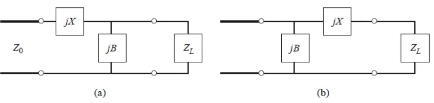
2.3.4 Matching Network
Impedance matching is often an important part of a larger design process for a microwave component or system. The basic idea of impedance matching is illustrated in Figure 2.2, which shows an impedance matching network placed between a load impedance and a transmission line. The matching network is ideally lossless, to avoid unnecessary loss of power, and is usually designed so that the impedance seen looking into the matching network is Z0. Then reflections will be eliminated on the transmission line to the left of the matching network, although there will usually be multiple reflections between the matching network and the load. This procedure is sometimes referred to as tuning. Impedance matching or tuning is important for the following reasons:
Maximum power is delivered when the load is matched to the line (assuming the
generator is matched), and power loss in the feed line is minimized.
Impedance matching sensitive receiver components (antenna, low-noise amplifier,
etc.) may improve the signal-to-noise ratio of the system.
Impedance matching in a power distribution network (such as an antenna array
feed network) may reduce amplitude and phase errors.
and performance of several types of practical matching networks. Factors that may be important in the selection of a particular matching network include the following:
Complexity—As with most engineering solutions, the simplest design that
satisfies the required specifications is generally preferable. A simpler matching network is usually cheaper, smaller, more reliable, and less lossy than a more complex design.
Bandwidth—Any type of matching network can ideally give a perfect match (zero
reflection) at a single frequency. In many applications, however, it is desirable to match a load over a band of frequencies. There are several ways of doing this, with, of course, a corresponding increase in complexity.
Implementation—Depending on the type of transmission line or waveguide being
used, one type of matching network may be preferable to another. For example, tuning stubs are much easier to implement in waveguide than are multisection quarter-wave transformers.
Adjustability—In some applications the matching network may require
adjustment to match a variable load impedance. Some types of matching networks are more amenable than others in this regard.
2.3.4.1 Matching with lumped element
In impedance matching network, they are several types of matching network such as lumped element matching, quarter wave matching and stub matching. For lumped element, it contain LC component. The L-section uses two reactive elements to match arbitrary load impedance to transmission line. For L element they are two possible
configurations will be illustrated in Figure 2.3. The smith chart is important part to design the matching network because from smith chart can determine the values of the
component wants.
If the normalized load impedance, zL = ZL/Z0, is inside the 1 + j x circle on the
Smith chart, then the circuit of Figure 2.4a should be used. If the normalized load
impedance is outside the 1 + j x circle on the Smith chart, the circuit of Figure 2.4b
should be used. The 1 + j x circle is the resistance circle on the impedance Smith chart for
which r = 1.
Figure 2.4: L-section matching networks. (a) Network for zL inside the 1 + j x circle. (b)
Network for zL outside the 1 + j x circle.
In either of the configurations of Figure 2.4 the reactive elements may be either inductors or capacitors, depending on the load impedance. Thus, there are eight distinct
inductors can be used. This may be feasible for frequencies up to about 1 GHz or so, although modern microwave integrated circuits may be small enough such that lumped elements can be used at higher frequencies as well. There is, however, a large range of frequencies and circuit sizes where lumped elements may not be realizable. This is a
limitation of the L-section matching technique. We will first derive analytic expressions
for the matching network elements of the two cases in Figure 2.4, and then illustrate an alternative design procedure using the Smith chart.
2.3.4.2 Matching with Quarter wave
Figure 2.5: The quarter wave matchin
Formula for characteristic impedance of quarter wave:
2.3.4.3 Matching with single stub
Figure 2.6: single stub tuning circuit. (a) shunt stub (b) series stub
The Smith chart of Figure 5.8 illustrates the basic operation of the double-stub tuner. As in the case of the single-stub tuner, two solutions are possible. The susceptance of the
first stub, b1 (or b’1, for the second solution), moves the load admittance to y1 (or y’1).
These points lie on the rotated 1 + jb circle; the amount of rotation is d wavelengths
toward the load, where d is the electrical distance between the two stubs. Then
transforming y1 (or y’ 1) toward the generator through a length d of line leaves us at the
The second stub then adds a susceptance b2 (or b’ 2), which brings us to the center of the
chart and completes the match. Notice from Figure 5.8 that if the load admittance, yL ,
were inside the shaded region of the g0 + jb circle, no value of stub susceptance b1 could
ever bring the load point to intersect the rotated 1 + jb circle. This shaded region thus
forms a forbidden
range of load admittances that cannot be matched with this particular double-stub tuner.
2.3.5 LNA parameters
This section introduces the important parameter used in the design theory of linear RF and microwave amplifier. Further, it develops some basic principle used in the
analysis and design of such amplifier. However, below is definitions that can apply to a single stage linear amplifier.
2.3.5.1 Gain
Three type of power gain in terms of the S parameter of the two-port network and the reflection coefficient, Гs and ГL, of the source and load:
(a) Power gain = G = P load / P input is the ratio of power dissipated in the load
ZL to the power delivered to the input of the two-port network. This gain independent of Zs, although some active circuits are strongly dependent on Zs.
(2.1)
(b) Available Gain = GA = Pavn/Pavs is the ratio of the power available from the two port network available from the source. This assumes conjugate matching of both the source and load, and depends on Zs but not ZL.
(c) Transducer Power Gain = GT = P load/ P avs is the ratio of the power
delivered to the load to the power available from the source. This depends on the Zs and ZL.
(2.3)
The operating gain design approach start from the desired load impedance and then the matches the resultant input impedance. The operating gain technique is recommended for linear-power amplifier, where the load is more important of the two terminations.
Amplifier design this way have only one match port (input port). Since the output port is not matched, the maximum small-signal gain cannot get, but that is the price to get maximum absolute output power.
Operating power gain, derived from the transducer gain is:
(2.4)
2.3.5.2 Stability and stability circle
In design LNA, need to consider the stability of transistor. The transistor was checking whether it is unconditionally stable or conditionally stable. The stability can define two types which are:
(a) Unconditional stability: The network is unconditionally stable if |Гin| < 1 and
|Гout| < 1 for all passive source and load impedances (i.e., |ГS| < 1 and |ГL | < 1).
(b) Conditional stability: The network is conditionally stable if |Гin| < 1 and |Гout| <
1 only for a certain range of passive source and load impedances. This case is also referred to as potentially unstable
Following conditions that must be satisfied by ГS and ГL if the amplifier is to be unconditionally:
If the device is unilateral (S12 = 0), these conditions reduce to the simple results that
|S11| < 1 and |S22| < 1 are sufficient for unconditional stability. For simpler test, the K − _ test, where it can be shown that a device will be unconditionally stable if Rollet’s condition and auxiliary condition
K= > 1 (2.7)
Figure 2.9: Output stability circles for a conditionally stable device. (a) |S11| < 1. (b)
|S11| > 1.
The output stability circle with a center:
2.3.5.3 Noise parameter
The noise factor, F of a noisy two port is defines as the ratio between the available signal-to-noise power ratio at the input to the available signal to ratio at the output.
The noise factor of the two ports can also be expressed in terms of the source admittance Ys=Gs+jBs as
When measuring noise, the noise factor is often represented in its logarithm from the noise figure,NF
NF= 10 log F
2.2.5.4 Noise Circle
Figure 2.10: Noise circle
2.3.5.5 DC biasing network
S-parameter of a device are fixed and do not age so long as the correct bias current is maintained. A drop in bias current, over life, will cause the RF device gain and output power to fall. Below are the descriptions of the bias network in the project:
a) A resistor bias network with a good results over moderate temperature changes was used instead of an active bias network because of its simplicity
b) The DC biasing network for this project will not be integrated with the RF printed circuit board. At low frequency, a bypassed emitter resistors an important contributor to the quiescent-point stability. At microwave
frequencies, the bypass capacitor, which is in parallel with the emitter resistor, can produce oscillations by making the input port unstable at some
CHAPTER 3
PROJECT METHODOLOGY
3.1 Introduction
Designing an LNA for lowest noise temperature requires knowing transistor noise parameters. Noise parameter can be obtain through a process that begins with measuring the S-parameter of a RF transistor and ends with using the circuit parameters of a FET model to calculate noise parameters. Since there is limitation to access a vector network analyser (VNA) to verify the S-parameter data on the manufacture data sheet, an assumption has to be made that all the data is accurate enough. But in this designing, we will not take transistor from datasheet. We will design the transistor instead of taking from datasheet.
The sensitivity of these receivers is often defined in terms of ―noise temperature‖, which equivalent to noise figure. In the design of practical amplifier, a stability consideration is essential in additional to those for gain and noise. For low noise, design of impedance matching networks around the transistor which optimizes the transistor the best noise performance. The main steps are summarized as following:
-Design of biasing networks
-Design of impedance matching networks
The design process is quite challenging because it involve in the distributed resistance, inductance and capacitance in the matching network. The design specification for this project as shown as below:
-Frequency: 5 GHz -Gain : >4dB
3.2 Design consideration
The following are the items that need to consider for design LNA. They are:
-Selection of the transistor -S-parameter for 5Ghz frequency -Stability of the transistor
-Gain (S-parameter)
-Noise figure (S-parameter)
3.2.1 Selection of the transistor
The FET transistor has been choosing to design LNA. The transistor is take from
manufacture and available in market. But this project will design using FET because the advantages are high gain, high linearity performance, low noise figure, and others. This project wills ATF-54143. This transistor is manufacture by Avago Technologies which offer excellent high performance at economical price. The combination of good gain, good noise and low noise make FET ideal for this project. The data sheet can referred at Appendix A.
3.2.2 Simulation of s-parameter using ADS software
3.2.3 Check the stability of the transistor
The stability of the transistor was checking based on Rollet’s condition and Auxiliary condition, �.
k>1 �<1
These two conditions are necessary and sufficient for unconditional stability, and are easily evaluated. In the project, the stability is consider unconditional stability because the device potentially stable and no oscillations will occur no matter what source and load reflection coefficient, Гs and ГL are presented.
Source and load reflection coefficient Гin and Гload respectively depend on load and source reflection coefficients as follows:
3.2.4 Gain (S-parameter)
S-parameters are valuable aid for collecting data for transistor and then using the data to predict performance and design the amplifier circuit. The values of s-parameter not only depend upon the properties of the transistor but also upon the source and load circuits used to measure them. This is because s-parameter values depend both upon the network and the characteristic impedance of the source and load used to measure it.
Several power gain equation appear in the literature which are equations (2.1), (2.2) and (2.3) are used through in the design of microwave amplifier.
3.2.5 Noise Figure
Noise figure, F of the two-port network is the ratio of signal-to-noise power ratio at the input to signal-to-noise ratio at the output. In other words, noise figure is a measure on how much a signal degrades as it passes through the two-port as a results of two-ports own noise. From the data sheet the minimum noise figure is 1db for frequency 900MHz. For frequency 5GHz the minimum noise figure still can get based on the calculation.
Noise figure also was calculated by using the equation 2.12 and 2.13 appeared in literature review.
3.3 Design of bias circuit
The necessary groundwork for designing an RF or microwave frequency amplifier has all been set. The first part of designing an amplifier is to find a circuit that will properly bias the RF transistor at the desired operating point but that will not interfere with the microwave operation of the circuit.
By biasing the ATF-54143 according to the measured specification data sheet’s S-parameter DC conditions, appropriate amplifier S-S-parameter can be achieved. For the ATF-54143, the performance of S-parameter over frequency (5GHz) is specified at Vce= 3V and Ic=60mA bias. DC voltage is 5 volt.
3.4 Design of matching network
CHAPTER 4
RESULT AND DISCUSSION
4.1 Calculation
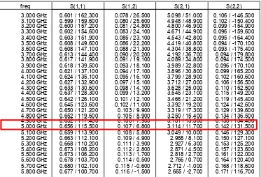
From data sheet of AVAGO Technologies (ATF-54143), the s-parameter is obtained from simulation as below:
freq
= | (0.656<115.5)(0.142<131.5) – (3.114<11.7) (0.107<6.8) |
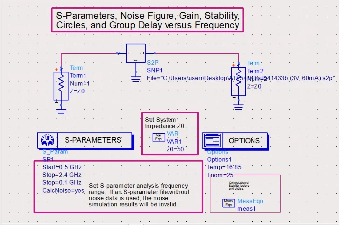
4.2 Simulation
Before designing any low noise amplifier (LNA) every designer has to check the stability of the device chosen for design. Manually, the calculations are very long but it is much quicker to simulate in any circuit simulating tool, for this ADS simulator was used to check the stability of the device and it was found that the selected ATF 54143 is potentially stable to the desired frequency at 5 GHz. To stabilize at frequency range between 4 GHz to 6 GHz. The Figure 20 and Table 3 show the stability at 5GHz frequencies.
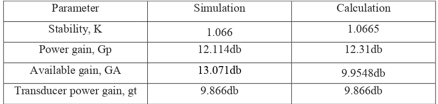
Table 4.3: comparison between simulation and calculation result
4.3 Negative feedback LNA and biasing
The technique for this LNA is using negative feedback amplifier. Below is the designing of circuit into ADS. It consists of active element such as Resistor (270ohm) and inductor (10nH). The simulation result show that low noise figure, stability k>1, high gain but bad return loss. Return loss can be fixed by design input and output matching network.
Parameter Simulation Calculation
Stability, K 1.066 1.0665
Power gain, Gp 12.114db 12.31db
Available gain, GA 13.071db 9.9548db
Figure 4.4: schematic diagram of negative feedback and biasing only
4.4 Matching Network
In designing the LNA, the RF input matching is almost the main part. Although it is the way to obtain the higher gain and better input return loss while to achieve the low noise figure an LNA design. Filter actually exists before the LNA have a poor input return loss, thus will affect the performance of the systems. Therefore, the goal for the input matching is to achieve good return loss and noise figure while maintaining acceptable gain. In this matching we decide to use single stub matching than lumped element. So this type of design will directly into microstrip line.
By using the ADS simulation we get the input matching by get the value of 5GHz frequency in source impedance (Zopt) required which achieve this noise figure, and the optimal load impedance for power transfer when the source impedance is Zopt. For best noise match (match for lowest noise figure but not best S11 return loss), need to match to Zopt.
Simulation based on output single stub matching:-
Same step like input single stub. We using design guide to generate the matching. The different is on the Zin and Zload data. Below is the information for output matching.
Figure 4.8: Schematic circuit of LNA at 1 stage
4.5 Optimization
The result shows that after matching and optimization. The optimization process well done when the matching network match with 50ohm. The optimization process tune by the parameter of input matching network which for magnitude S11 and magnitude for S22. This magnitude refers as reflection coefficient.
Then, after matching network being constructed in a microstrip line, it is built in electrical transmission line which can be fabricated using printed circuit board
technology. At the end at the input impedance we adjusting the value and determine it by tuning the component such as MLIN, MTEE and etc.
4.5.1 1st stage schematic simulation result
Figure 4.11: simulation result of gain and return loss 1stage LNA
4.5.2 3 stage schematic simulation result
Figure 4.13: schematic diagram of 3stage LNA
Figure 4.15: simulation result of noise figure 3stage LNA
Parameter 1st stage 3rd stage
Gain (S2,1) 9.653dB 21.752dB
Return loss (S1,1) -27.434dB -25.748dB
NF min 2.111 2.619
Table 4.16: Comparison table between 1st stage and 3rd stage negative feedback LNA schematic
The value that were obtained is an optimized value, based on the table the value of S21 on 3-stage cascade single stage amplifier is more stable than 1-stage. More gain is occur when cascade the 1-stage but the return loss and noise figure is lower than 1-stage result. But both stage follows design specification that mention before in chapter 3. So, both stage are accepted to proceed next step to layout simulation. In schematic
4.5.3 1 stage layout simulation result:
Figure 4.17: Layout of 1 stage LNA
Figure 4.19: result of simulation 1st stage layout
4.5.4 3rd stage layout simulation result:
Figure 4.20: Layout of 3 stages LNA
Figure 4.22: result of simulation 3stage layout LNA
parameter 1st stage 3rd stage
Gain (S2,1) 7.297dB 23.527dB
Return loss (S1,1) -30.078dB -10.504dB
NF min 2.864 3.385
Impedance matching 52.178+j2.349 68.061+j31.694
Stability factor 1.160 1.487
Table 4.23: Comparison table between 1st stage and 3rd stage negative feedback LNA layout
Before, we already simulate and tuning to make the best result in 4.4.1 and 4.4.2. Now, in layout simulation there will be varying of result because of some factor. In layout we need to consider every part of the circuit because from layout we will fabricate the LNA. Usually people will add some of the microstrip line (MLIN,MCORN & MTEE) to fulfil the design because in the schematic is not ideal and not possible to fabricate with the design. From schematic, we will generate the layout. Then we will adjust the layout follow the schematic drawing. The gap is already determined from the schematic
From the observation above, we can see that the 3-stage LNA result 3x higher in gain compared to 1-stage but the return loss shows drawback. The noise figure also quite higher compare to schematic simulation.1-stage LNA circuit shows a good impedance matching than 3-stage because nearest to 50ohm. Both LNA shows a stable circuit where the K>1.
4.6 Fabrication and Measurement
The file from ADS software is taken to Coral Draw software con figure for milling and fabrication process. After checking all dimensions and final adjustment, the fabrication was done by using machine provided in PSM laboratory in FKEKK UTeM. After milling and drilling and plating processes, the LNA is completed by adding the test port SMA connectors for measurements. The dimensions of fabricated LNA are6x3cm for 1-stage and 8x3 cm for 3-stage. After fabrication process, the LNA is measure by using Agilent Network Analyzer.
Figure 4.25: Fabricated 3-stage LNA
In order to test the device low noise amplifier which are using Agilent Network Analyzer to determine the S-Parameter. To testing the device should be the voltage input is given 5VDC to protect the design of the LNA excessive current draw due to layout circuit. Before use the analyzer, calibration must be done.
Figure 4.27: Voltage Input 5V DC for biasing circuit
Figure 4.28: The S-parameter measurement results for 1stage
4.7 Debugging and Final LNA Measurement
Initial result showed that the return loss needs improvement (Fig.) Main reason appeared that the LNA was not well grounded on the side edges in the beginning, vias were not well filled with conducting paste. Moreover, we deal with the SMD component which very small in size. The normal soldering tools is not suitable for SMD type. Maybe human error while solder causes the measurement to be different from simulation.
As we can see there is no gain in the measurement. After meeting with supervisor, I have found the mistake of my soldering. The FET may be short because of the debugging while soldering. I am using iron clamps to hold the FET but not covering my hand. So my body becomes electrostatic static discharge make the component short.
CHAPTER 5
CONCLUSION
5.1 Conclusion and Future Network
As a conclusion 5GHz frequency formally is unique in that, in all cases, the authorized unlicensed spectrum spans several GHz which in cover for WLAN
application. Furthermore, it’s a new spectrum that been used to avoid a crowd in 2.4GHz spectrum.
In order to design LNA, the transistor that are using is ATF-54143 which is commonly cover from 450MHz till 6GHz. This transistor has good features in Avago Technologies. From the simulation, the parameter that have been target is achieved which is noise figure less than 2.5dB, gain more than 4dB and return loss is less than -10dB. The simulation is at 5GHz.
REFERENCES
[1] David M. Pozar, Microwave and RF Wireless System, John Willey & Sons, Inc. Third Edition, 2000. Chapter-10
[2] Kalavakuru, Sivadeep Reddy ―LOW NOISE AMPLIFIER (LNA) DESIGN‖ School Of Engineering and Computer Science, Syracuse University
[3] Matthaei, L. George, Young, Leo, Jones, ―Microwave Filters, Impedance- Matching Networks and Coupling Structures‖, McGraw-Hill 1980, ISBN 0- 89006-099
[4] N. Ahsan, A. Ouacha, J. Dabrowski and C. Samuelsson ―Dual band Tunable LNA for Flexible RF Front-End,‖ International Bhurban Conference on Applied Sciences & Technology, pp 19-22, January 2007.
[5] K. Datta, R. Datta, A. Dutta, T.K. Bhattacharyya, ―PSO based Output Matching Network for Concurrent Dual-Band LNA‖, IEEE International Conference on Microwave and Millimeter Wave Technology, May 2010.
[8] Federal Communications Commission. ―Authorization of Spread Spectrum
Systems Under Parts 15 and 90 of the FCC Rules and Regulations". 18 June, 1985. Retrieved 2007-08-31.
[9] Gonzalez, Guillermo. Microwave transistor amplifiers: analysis and design. Vol. 2. New Jersey: Prentice hall, 1997
[10] Data Sheet, AVAGO Technologies, ATF- 58143, Visited date: 17 August, 2012 http://www.avagotech.com/
[11] H. J. Lee, D. S. Ha, and S. S. Choi, ―A 3 to 5 GHz fet UWB LNA with input matching using Miller effect,‖ IEEE Solid-State Circuits
Conf., pp. 731–740, February 2006.
[12] S. Ock, K. Han, J. Ryul Lee and B. Kim, ―A Modified Cascade Type Low Noise Amplifier Using Dual Common Source Transistors‖, IEEE International
Microwave Symposium Digest, pp. 1423– 1426, Aug. 2002
[13] H.J. Lee, Dong. S. H, S. S. Choi, "A 3 to 5GHz UWB LNA with Input Matching using Miller Effect", IEEE Solid-State Circuits Conf., 2006. [14] Andres Moran Valerio, Alonso Perez Garrido, Thesis title ―Design and Implementation of 6-8.5 GHz LNA‖, Institute of Science & Technology, Linkoping University, 2008-11-07,pp. 13
[15] Adriana Serban Craciunescu, ―Low-Noise Amplifier for Ultra-Wideband System‖. LiUTEKLIC- 2006.