A Low Profile Switchable Pattern Directivity
Antenna using Circular Sectorized EBG
M.S.M.Isa
1,2, R.J.Langley
2, S.Khamas
2, A.A.M.Isa
1, M.S.I.M.Zin
1, Z.Zakaria
1, N.Z.Haron
1, A. Ahmad
31Centre for Telecommunication Research and Innovation (CeTRI), Faculty of Electronic and Computer Engineering,
Universiti Teknikal Malaysia Melaka, Melaka, Malaysia
2Department of Electronics and Electrical Engineering, University of Sheffield,
Sheffield S1, United Kingdom 3
Faculty of Information and Communication Technology, Universiti Teknikal Malaysia Melaka, Melaka, Malaysia
Abstract— In this paper, a low profile patch antenna switchable radiation pattern diversity with total thickness of
OHVV WKDQ Ȝ0/14 has been established.. The novel antenna structure is based on a conformal patch antenna operating in TM01 mode is integrated over an electromagnetic band gap (EBG) surface to provide a beam scanning antenna. The circular EBG elements are arranged in 6-sectors and the vias on each sector of the EBG are switched in and out to steer the beam into that sectors. The reflection coefficients for the antenna when the vias are switched remain stable. The simulation and experimentation results have shown that the antenna power pattern directed toward the sector, without via or the middle of sectors, without via. Overall a flexible low profile beam steering antenna is demonstrated. The antenna is designed for wireless network application especially to improve the system performance in multipath propagation environment. Furthermore, the low profile antenna makes it suitable to be used in vehicular application.
Index Terms—EBG, pattern directive, low profile, beam scanning, vehicular application.
I. INTRODUCTION
Human body monitoring system normally consists of several sensors and gadget which connected to control system either by wire or wireless. Wired communication gives more efficiency and bandwidth but with some limitation such as distance and comfortableness. Wireless communication system is more comfortable and tidier but might face limitation of signal fading or complete loss of signal [1].
Mobile communication system in multipath propagation environment has the fast fading problem which gives a significant impact on the overall system performance. The fading occurs when the signal arrive at receiver over different path, hence different in amplitude and phase. The total signal vector at the receiver is taken from the vector simulation of all the received signals, which usually contains significant signals, fade and pattern interference. The most popular technique to combat the signal fading is known as diversity [2, 3] . Multiple incoming signals are combined properly in order to increase the probability and strength of the received signal.
Electronic band gap (EBG) was used to alter the surface characteristic for diversity antenna. Various surface wave
antennas have been developed using the advantages of EBG structure. The EBG also contributed in reducing overall antenna size and improved in overall performance [4, 5].
Further understanding of the diversity criteria will be very useful for the research development. Various types of diversity antenna such as pattern diversity, polarization diversity, spatial diversity, transmit/receive diversity, time diversity and frequency diversity are commonly used to combat signal fading in wireless communication.
A. Electromagnetic Bang Gap
Electromagnetic band gap surface which known as high impedance surface is among the popular study for band gap application in wireless environment. The previous design of EBG has found to be larger in size as the period was designed at half wavelength which might be inconvenient to accommodate with antenna and circuit especially on space constraint environment.
The EBG has been found to be effective in improving the antenna performance when placed on top of the structure. The front-to-backward ratio of the antenna has been enhanced by introducing EBG under or around the antenna [6, 7]. The mutual coupling of the array antenna has been found to be reduced by combining the EBG in the designed [8-12].
The size of the EBG also reduced by introducing EBG with mushroom type structure with connection via within EBG and ground surface. In early finding, the EBG structure period was reduced by 10% with respect to free space phenomena [4]. In various designs, the surface wave propagation can be simplified by laminated structure dielectric which works as a dielectric waveguide.
For surface wave antenna technology, the EBG without via which sometime known as artificial ground has been widely used in antenna design and fabrication [13]. The circuit to tune and limit the frequency as in [14] can be utilised.
B. Band Gap Resonant Frequency and Bandwidth
The resonant frequency for the EBG structure is specified
electromagnetic properties were simplified onto series of lumped circuit elements, which are capacitors and inductors.
The capacitance, Cis normally due to the gap within the
element and the inductance, Lhas been produced due to
current flow through via to ground plane [9].
With the smaller size of period compared to the wavelength, the wave impinging on the material has caused the electric field to span over the narrow gap within the
patch, which introduced the sheet capacitance, C. The
current oscillated between neighbouring patches through via
which connected to ground has induced sheet inductance, L
in the circuit. These phenomena have formed the parallel
resonant circuit which dictates the material’s
electromagnetic behaviour. At any frequency, the surface impedance has been defined as [4]
LC
At resonant frequency, the surface impedance will become infinite and the resonant frequency of the EBG can be represent as
The surface has shown the artificial magnetic conductor
at LCresonant frequency, where the reflection phase was
zero degree [4]7KHUHIOHFWLRQZDVYDULHGIURPʌ/2 to –ʌ/2,
which represents the antenna bandwidth and cross through at zero for resonance centre frequency. For thin structure with nonmagnetic material (
o
P
P ) the bandwidth of the
resonance has been limited by the thickness,tdivided by
radiance length at resonance,r0which can be summarised as
[4]
o r
t
Bd (1.4)
The resonant frequency and bandwidth of the texture can be tuned by changing the inductance or capacitance or both values [11, 15]. The sheet inductance value can be changed by varying magnetic permittivity or the material thickness, which is normally fixed and difficult to be tuned. The capacitance however is easier to be varied by the metal arrangement and geometry [16, 17] or by adding lumped elements or tuneable varactor diodes onto the texture [7, 15, 18-20].
Mechanically, the frequency response with respect to capacitance can be changed by moving the tuning surface against stationary surface, whereas the phase gradient has been produced by rotating it, which steered the reflected beam [16, 17].
Electrically, the mechanical moving plate was replaced with a voltage tuneable varactor diode. By adjusting the
reverse-biased voltage supplied to the diodes, the capacitance within each plate will be adjusted, which tunes the antenna resonance frequency. In order to eliminate the interference to magnetic field at the front surface the bias lines were connected from behind of the surface. In some researches, the change in varactor diode capacitance value, has made steerable reflection beam possible [15, 18-20].
C. Surface Wave Antenna
Surface wave antenna (SWA), has been designed to make use of the surface wave propagation. Various theories and experimental results have been reported since the SWA concept was introduced in the 1950’s [21-26]. Various designs and shapes have been implemented on the metal in order to enable surface wave propagation.
Meta-material and electromagnetic surface design and development have contributed in the evolvement of surface wave antenna. The SWA application has been conducted where the low profile monopole like antenna as in [27-30] has been conducted. The monopole-like dual-band SWA has been realized in [31] with the advantage of a low profile configuration.
The low profile surface wave antenna is suitable to be applied for vehicular application, as the antenna design was always dictated by the vehicle style, due to conformable requirement according to the vehicle metallic body. The distance from metallic body has been kept to maximum as closer distance reduces efficiency and radiation pattern shape as it effects the excitation on surface current. In [29, 32] , the low profile antenna was developed based on high-impedance surface, which shield the surface wave effect.
D. Diversity Antenna
In wireless communication transmission mainly, the received signal sometimes is effected by channel impairment problem which greatly due to multipath propagation. The effect of multipath in the communication system implies great variation in the RF system, with signal fading and sometime complete loss of the signal. Diversity antenna is strongly recommended in reducing the effect of multipath and interference. The directional pattern can also be made possible using diversity technique [32, 33]. In [34, 35], the diversity antenna with radiation pattern directivity and low correlation coefficient has been designed. The miniature PIFA antenna as in [36], has also given small correlation coefficient.
The diversity antenna has been widely used for radiation pattern diversity and MIMO application [37, 38]. The parasitic diversity antenna as in [39, 40] has been used for pattern diversity where the array of parasitic antenna has been switched for power directive pattern.
The assembly of antenna and virtually sectorized EBG structure has been used to control the power pattern directivity. This capability will enable the future development of the pattern diversity antenna for wireless and vehicular application [41, 42].
II. PATTERN DIRECTIVITY ANTENNA
Multiple monopoles parasitic antenna which placed around antenna has been used for directing the radiation direction or power direction finding [40, 43]. The direction of pattern was found by alternately switching the parasitic antenna to specific direction or direction with highest radiation power. The designs required multiple antennas and high in profile as monopole antenna was used.
In this paper, the analysis for circular sectorized EBG power pattern directivity has been published. The circular EBG structure has been used for directing the antenna around the antenna. For notification purposes, the circular EBG structure has been virtually divided into six sections for power pattern directional purposes as shown in Fig. 1.
The EBG with pin vias which inserted from the patches to the ground plane have been designed to have a stop band at 2.2 GHz. An EBG structure with a diameter of 175.7mm has been designed by simulation on FR4 printed circuit and consists of 17.4mm diameter circular patches that have been arranged along 6-sectors labelled as A to F. Each one of these sectors has pin vias that can be switched on or off. Fig.1 shows the arrangement of EBG with sector-A without pin via.
The mutual coupling of the surface was simulated and analysed. The combination of EBG and artificial ground sectors on the circular structure was expected to be able to reject or propagate the surface wave respectively.
The EBG sectors characteristic has been altered using pin vias which capable to increase isolation within surface and EBG without via has propagated the wave through the surface. Analysis of the EBG surface characteristic has been conducted using a transmission line method as in [5] The transmission coefficient between the ports of the
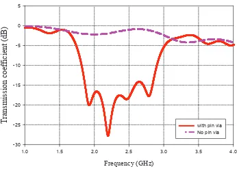
transmission line, which placed over the EBG surface, has been used to measure the transmission characteristics of the EBG surface. Fig. 2 illustrates the simulated transmission results for the circular EBG. Simulations have been conducted for the cases of the EBG with pin vias and when all the pin vias are removed. These results illustrate a stop band at 2.2 GHz when pin vias are inserted and a pass band at the same frequency when the pin vias are removed. The finding is essential to analyse the EBG surface characteristic to steer the radiation pattern around the antenna.
A. Simulation Result for Pattern Directivity using Sectorized EBG.
The arrangement of circular patch antenna above circular EBG structure is shown in Fig. 3. The circular antenna has been designed using an FR4 printed circuit board with a diameter of 115.4mm and a 3.2mm thickness. The antenna has been placed at 3mm above the EBG surface and a metal pin, with a diameter of 1mm, has been used to connect the antenna to the discrete port that is placed underneath the
substrate. The total thickness of the antenna is
approximately 9.4mm which is less than
Ȝ
2.2GHz/
14.For analysing the EBG capability to control the wave propagation around the antenna, the pin via in each sector has been alternately switched in and out. Fig. 4 presents the return losses for patch antenna under four scenarios, which corresponds to an antenna with all the pin vias in place except for sector-A, sector-F, A&D and sectors-A&F. It can be noticed from the results that the antenna operating frequency is stable around 2.2 GHz for all configurations. Another narrow band is noticed at 1.5 GHz which attributed by the effect of integrating the antenna with EBG which slightly increased the structure total cavity. However the band has not been considered as the band is very narrow and outside the antenna and EBG desired operating range.
Fig 1: Circular EBG in 6-sectors configuration
(sector-A without pin via) x
y
Frequency (GHz)
1.0 1.5 2.0 2.5 3.0 3.5 4.0
T
ra
n
sm
is
si
o
n
c
o
ef
fi
ci
en
t
(d
B)
-30 -25 -20 -15 -10 -5 0 5
with pin via No pin via
Fig. 2: Transmission coefficient, S21within circular EBG
Fig. 3: Simulated diagram for circular antenna 3mm above EBG surface
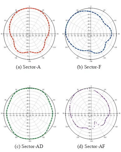
To study the EBG capability to control the antenna power pattern directivity, the pattern has been studied at 2.2GHz with various arrangements of EBG’s sector/s pin vias switching. The azimuth radiation has been observed. For the pattern as described in Fig. 5, the relative azimuth patterns
EHHQ PRQLWRUHG DW WKHWD Û ZKLFK UHSUHVHQWV WKH DQWHQQD
surface wave radiation.
The radiation patterns demonstrate that the power has been directed towards the sector in which the pin vias are removed. For example in Fig. 5(a), where the pin vias have been removed from sector-A, the power is directed along that direction of phi=0°, while removing the pin vias from sector-F shifts the power in the direction of phi=60°. In both cases the maximum gain increases by approximately 13dB. The side lobes of the radiation patterns are also decreased by approximately 10dB, which demonstrates that the surface wave is well propagated towards the higher surface transmission sectors and reflected by the EBG structure with lower transmission coefficient. For the case of multiple sectors, for example of A&D and A&F as shown in Fig. 5(c) and (d) the pattern is directed toward the both sectors for the case of A&D and to the middle of the combination sectors for the case of A&F.
The sectorized power distribution also occurs for all the other sectors. In addition, if pin vias from two sectors of the EBG are removed the pattern again points in the direction away from those sectors, which allows a very flexible beam steering options. The shape of the patterns for the sector-D almost duplicating the pattern for sector-A, whereas for the case of sector-E, C or B, the pattern almost similar to pattern for sector-F but directing to the specific sector. The pin switching can be done either using individual switch of diode or MEMs switches or group switching using switch board as introduced in [44].
-40 -35 -30 -25 -20 -15 -10-50
Fig.5: Azimuth (xy-plane) plane normalized patterns at 2.2GHz with pin vias switched out at
(a) sector-A and (b) sector-F (c) sectors A&D (d) sectors A&F
Frequency (GHz)
B. Fabrication and Measurement
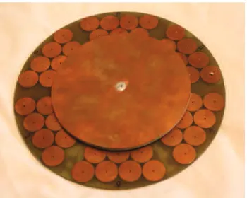
For the measurement purposes, the circular patch antenna has been fabricated by using a single sided FR4 printed circuit board with a diameter of 115.4mm as shown in Fig. 6. The EBG substrate has been fabricated using a double sided FR4, which has been cut into a circular shape with a diameter of 175.7 mm. The EBG pattern with a circular patch diameter of 17.4 mm has been etched onto the top side of the PCB, whereas the conducting ground plane has been positioned at the bottom side of the substrate. The circular patch antenna and EBG has been fabricated and assembled with about 3mm gap between the antenna PCB and the EBG surface as shown on Fig. 3. The gap has been achieved using
a Rohacell substrate with
İ
r=1.06 and a 3mm thickness hasbeen used to keep the constant gap within the elements. The antenna was placed at the middle of EBG structure as shown in Fig 6. A 1mm radius hole has been drilled through the EBG substrate for inserting the 1mm radius connection pin which connecting the antenna patch to the excitation
SRUW 7KH SRUW ZLWK LQSXW LPSHGDQFH RI KDV EHHQ
connected at underneath the EBG structure. The antenna total thickness is only approximately 9.4mm, which determines the low profile characteristic of the antenna.
The return loss, S11 for the antenna has been measured
using an 8720D Hewlett Packard network analyser, which can be used over a frequency range of 50MHz to 20GHz. Measurements of the antenna farfield pattern have been carried out in an anechoic chamber. The measurements for the antenna’s reflection coefficient and power pattern have been done for the various sectors arrangement and results are shown on Fig. 7 and 8 respectively.
The comparisons of the simulated and measured return loss are as shown in Fig. 7 for pin vias switching in sectors A, F, A&D, and A&F. The experimental results have been obtained with a frequency shift of 200 MHz compared to simulation, but the main operating band near 2.2 GHz is well defined. The narrow band near 1.5 GHz in the simulation was not observed in the measurements. The discrepancy between simulation and measurements can be attributed to the measurement tolerances as well as fabrication, equipment and antenna set up errors.
The antenna surface radiation pattern has been measured with various switching configuration for the pin vias in the EBG sectors has been measured inside anechoic chamber. The measured and simulated antenna normalised radiation pattern are shown in Fig.8.
The radiation patterns as shown in Fig. 8 for the cases of pin via switched out from sectors A, F, A&D and A&F respectively have directed towards the sector/s or direction within sectors for case of A&F sectors. For the case of all sectors without pin vias, the radiation pattern is circular around the antenna which shows the effectiveness of the sectors to propagate the power. Good agreement has been achieved between the simulated and measured results with the increased power and direction of the patterns being confirmed.
Therefore, it can be concluded that, the sectors with via can be used to direct the power patterns accordingly. This configuration might be used in conjunction with power pattern diversity antenna. Various and flexible switching of the sectors can be simplified by group switching using switch board [44]. Again results for various combinations of sectors confirm the overall flexibility of the beam scanning by the EBG sector.
III. CONCLUSION
A conformal patch antenna, which has been placed over a circular EBG that consists of 6-sectors, with total thickness
of less than
Ȝ
2.2GHz/
14 has demonstrated a flexible andcontrollable beam steering. Pin vias, which are placed at the middle of each circular patch element of the EBGs, have been used to switch the bandgap surface characteristics. Fig.6: Antenna and EBG Assembly
Frequency (GHz)
Switching pin vias in and out at each sector has established the EBG capability to control the antenna beam direction with increasing the gain by about 13dB. The antenna reflection coefficients remain fairly stable as the pin vias in EBG’s sector switched in and out. The beam has been scanned around the antenna by alternately switching the sectors which demonstrates the antenna flexibility. The experimental results for the circular EBG integrated with a patch antenna have confirmed the findings of the simulations. This novel development would be very useful for wireless application especially when pattern diversity antenna is required. The low profile antenna in other hand can be useful for the antenna to be utilised in vehicular application to suit the conformable requirement.
ACKNOWLEDGMENT
The authors would like to thank University of Sheffield for their facilities. Great gratitude to Universiti Teknikal
Malaysia Melaka (UTeM) and Ministry of Higher
Education for their “Research Acculturation Grant: RAGS/2012/FKEKK/TK02/2 B0005“.
REFERENCES
[1] C. A. Balanis, Antenna Theory, Analysis and Design, 3rd ed. New
Jersey: John Wiley & Sons, Inc, 2005.
[2] R. G. Vaughan and J. B. Andersen, "Antenna diversity in mobile
communications," IEEE Transactions on Vehicular Technology, vol.
36, pp. 149-172, 1987.
[3] R. Vaughan, "Switched parasitic elements for antenna diversity,"
IEEE Transactions on Antennas and Propagation, vol. 47, pp. 399-405, 1999.
[4] D. Sievenpiper, Z. Lijun, R. F. J. Broas, N. G. A. A. N. G.
Alexopolous, and E. A. Y. E. Yablonovitch, "High-impedance
electromagnetic surfaces with a forbidden frequency band," IEEE
Transactions on Microwave Theory and Techniques, vol. 47, pp. 2059-2073, 1999.
[5] M. S. Mohamad Isa, R. J. Langley, S. Khamas, A. Awang Md Isa, M.
S. I. M. Zin, F. M. Johar, and Z. Zakaria, "Antenna Beam Steering
using Sectorized Square EBG," Journal of Telecommunication,
Electronic and Computer Engineering (JTEC), vol. 4 No 1, pp. 39-44, 2012.
[6] R. Gonzalo, P. De Maagt, and M. Sorolla, "Enhanced Patch-Antenna
Performance by Suppressing Surface Waves Using Photonic-Bandgap
Substrates," IEEE Transactions on Microwave Theory and
Techniques, vol. 47, pp. 2131-2138, 1999.
[7] D. F. Sievenpiper, "Forward and backward leaky wave radiation with
large effective aperture from an electronically tunable textured
surface," IEEE Transactions on Antennas and Propagation, vol. 53,
pp. 236-247, 2005.
[8] H. Xin, K. Matsugatani, M. Kim, J. Hacker, J. A. Higgins, M. Rosker,
and M. Tanaka, "Mutual Coupling Reduction of Low-Profile
Monopole Antennas on High-impedance Ground Plane," Electronics
Letters, vol. 38, pp. 849-850, 2002.
[9] Y. Fan and Y. Rahmat-Samii, "Microstrip Antennas Integrated With
Electromagnetic Band-Gap (EBG) Structures: A Low Mutual
Coupling Design for Array Applications," IEEE Transactions on
Antennas and Propagation, vol. 51, pp. 2936-2946, 2003.
[10] Y. Yuan, W. Xin, and F. Zhenghe, "A Novel dual-band Compact Electromagnetic Bandgap (EBG) Structure and its Application in
Multi-antennas," IEEE Antennas and Propagation Society
International Symposium, pp. 1943-1946, 2006.
[11] M. S. Mohamad Isa, R. J. Langley, S. Khamas, A. Awang Md Isa, M. S. I. M. Zin, F. M. Johar, and Z. Zakaria, "Microstrip Patch Antenna Array Mutual Coupling Reduction using Capacitive Loaded
Miniaturized EBG," Journal of Telecommunication, Electronic and
Computer Engineering (JTEC), vol. 4, pp. 27-34, 2012.
[12] M. S. Mohamad Isa, R. J. Langley, S. Khamas, A. Awang Md Isa, M. S. I. M. Zin, Z. Zakaria, N. Z. Haron, and A. Ahmad, "A Novel Technique of Controlling Signal Propagation within Array Elements
using Switchable Miniaturized Electromagnetic Band Gap," 2013
IEEE Symposium on Wireless Technology & Applications (ISWTA),
[13] A. Foroozesh and L. Shafai, "Application of Combined Electric- and Magnetic-Conductor Ground Planes for Antenna Performance
Enhancement," Canadian Journal of Electrical and Computer
Engineering, vol. 33, pp. 87-98, 2008.
[14] Z. Zakaria, N. H. Ali, M. S. Mohamad Isa, and A. Awang Md Isa, "Design of Frequency Limiting Circuit Based on Nonlinear Matched
Reflection-Mode Bandstop Resonator," Journal of
Telecommunication, Electronic and Computer Engineering (JTEC), vol. 4, pp. 57-62, 2012.
[15] D. F. Sievenpiper, J. H. Schaffner, H. J. Song, R. Y. Loo, and G. Tangonan, "Two-dimensional beam steering using an electrically
tunable impedance surface," IEEE Transactions on Antennas and
Propagation, vol. 51, pp. 2713-2722, 2003.
[16] D. Sievenpiper, J. Schaffner, J. J. Lee, and S. Livingston, "A steerable
leaky-wave antenna using a tunable impedance ground plane," IEEE
Antennas and Wireless Propagation Letters, vol. 1, pp. 179-182, 2002. [17] D. Sievenpiper, J. Schaffner, R. Loo, G. Tangonan, S. Ontiveros, and R. Harold, "A tunable impedance surface performing as a
reconfigurable beam steering reflector," IEEE Transactions on
Antennas and Propagation, vol. 50, pp. 384-390, 2002.
[18] S. V. Hum, M. Okoniewski, and R. J. Davies, "Realizing an electronically tunable reflectarray using varactor diode-tuned
elements," IEEE Microwave and Wireless Components Letters, vol.
15, pp. 422-424, 2005.
[19] M. Sonkki, M. Berg, J. Pihlaja, S. Karhu, H. Jantunin, and E. Salonen,
"Varactor Tunable Helical Antenna," The Second European
Conference on Antennas and Propagation (EuCAP), pp. 1-6, 2007. [20] C. Mias and Y. Jyh Haur, "A Varactor-Tunable High Impedance
Surface With a Resistive-Lumped-Element Biasing Grid," IEEE
Transactions on Antennas and Propagation, vol. 55, pp. 1955-1962, 2007.
[21] C. Tai-Lee and L. Yu-De, "Surface-wave effect between leaky-mode
microstrips," 2005 IEEE Antennas and Propagation Society
International Symposium, vol. 1B, pp. 434-437, 2005.
[22] R. Elliott, "Spherical surface-wave antennas,"IRE Transactions on
Antennas and Propagation, vol. 4, pp. 422-428, 1956.
[23] L. Felsen, "Radiation from a tapered surface wave antenna," IRE
Transactions on Antennas and Propagation, vol. 8, pp. 577-586, 1960. [24] G. Fikioris, R. W. P. King, and T. T. Wu, "Novel surface-wave
antenna," IEE Proceedings -Microwaves, Antennas and Propagation,
vol. 143, pp. 1-6, 1996.
[25] R. Hougardy and R. Hansen, "Scanning surface wave
antennas-Oblique surface waves over a corrugated conductor," IRE
Transactions on Antennas and Propagation, vol. 6, pp. 370-376, 1958. [26] J. P. Kim, C. W. Lee, and H. Son, "Analysis of corrugated surface
wave antenna using hybrid MOM/UTD technique," Electronics
Letters, vol. 35, pp. 353-354, 1999.
[27] F. Yang, Y. Rahmat-Sami, and A. Kishk, "Low-profile patch-fed
surface wave antenna with a monopole-like radiation pattern," IET
Microwaves, Antennas & Propagation, vol. 1, pp. 261-266, 2007. [28] F. Yang, Y. Rahmat-Samii, and A. Kishk, "A novel surface wave
antenna with a monopole type pattern: a thin periodically loaded slab
excited by a circular disk," 2005 IEEE Antennas and Propagation
Society International Symposium, vol. 1A, pp. 742-745, 2005. [29] Y. Fan, A. Aminian, and Y. Rahmat-Samii, "A low profile surface
wave antenna equivalent to a vertical monopole antenna," 2004 IEEE
Antennas and Propagation Society International Symposium, vol. 2, pp. 1939-1942, 2004.
[30] A. Al-Zoubi, Y. Fan, and A. Kishk, "A Low-Profile Dual-Band
Surface Wave Antenna With a Monopole-Like Pattern," IEEE
Transactions on Antennas and Propagation, vol. 55, pp. 3404-3412, 2007.
[31] Y. Fan, A. Al-Zoubi, and A. Kishk, "A Dual Band Surface Wave
Antenna with a Monopole Like Pattern," 2006 IEEE Antennas and
Propagation Society International Symposium, pp. 4281-4284, 2006. [32] D. Sievenpiper, H. P. Hsu, J. Schaffner, G. Tangonan, R. Garcia, and
S. Ontiveros, "Low-profile, four-sector diversity antenna on
high-impedance ground plane," Electronics Letters, vol. 36, pp. 1343-1345,
2000.
[33] D. V. Thiel and S. Smith, Switch Parasitic Antenna For Cellular
Communiction, 1st. ed. London: Artech House, 2002.
[34] S. Hosono, N. Goto, and H. Arai, "A flat diversity antenna by disk
loaded monopole and three notches," IEEE Transactions on Vehicular
Technology, vol. 43, pp. 353-358, 1994.
[35] M. S. Mohamad Isa, R. J. Langley, and S. Khamas, "Antenna pattern
diversity using EBG," Loughborough Antennas and Propagation
Conference (LAPC), 2010, pp. 325-328, 2010.
IEEE Antennas and Wireless Propagation Letters, vol. 8, pp. 49-53, 2009.
[37] B. A. Cetiner, J. Y. Qian, S. Liu, L. Jofre, G. P. Li, and F. De Flaviis, "A compact wideband MEM switched diversity antenna for indoor
mobile channels," IEEE MTT-S International Microwave Symposium
Digest, vol. 3, pp. 1711-1714, 2003.
[38] S. B. Yeap, X. Chen, J. A. Dupuy, C. C. Chiau, and C. G. Parini,
"Low profile diversity antenna for MIMO applications," Electronics
Letters, vol. 42, pp. 69-71, 2006.
[39] C. Wenhua, B. Bing, and F. Zhenghe, "Low profile parasitic antenna
array of monopole by using dielectric resonator ring," 6th
International Symposium on Antennas, Propagation and EM Theory, pp. 198-201, 2003.
[40] A. Khaleghi, J. C. Bolomey, and A. Azoulay, "A Pattern Diversity Antenna with Parasitic Switching Elements for Wireless LAN
Communications," 2005. 2nd International Symposium on Wireless
Communication Systems, pp. 611-615, 2005.
[41] A. A. M. Isa, G. Markarian, M. S. M. Isa, Z. Zakaria, and M. S. I. M. Zin, "Simulation of virtual MIMO base stations for mobile location in
IMT-Advanced networks," IEEE Asia-Pacific Conference on Applied
Electromagnetics (APACE), 2012, pp. 176-181, 2012.
[42] A. Awang Md Isa, G. Markarian, M. S. Mohamad Isa, N. Haron, and M. Zin, "Hybrid TOA-Based MIMO and DOA-Based Beamforming
for Location and Positioning in WiMAX Networks," Journal of
Telecommunication, Electronic and Computer Engineering (JTEC), vol. 4, pp. 11-20, 2012.
[43] T. Svantesson and M. Wennstrom, "High-resolution direction finding
using a switched parasitic antenna," Proceedings of the 11th IEEE
Signal Processing Workshop on Statistical Signal Processing, 2001., pp. 508-511, 2001.
[44] M. S. Mohamad Isa, R. J. Langley, and S. Khamas, "Antenna control
using EBG," Proceedings of the 5th European Conference on