AC VOLTAGE REGULATION OF A BIDIRECTIONAL HIGH-FREQUENCY
LINK CONVERTER USING A DEADBEAT CONTROLLER
L. S. Toh, M. Z. Ramli, and Z. Salam
Malik E. Elbuluk
Faculty of Electrical Engineering Department of Electrical and Computer Engineering Universiti Teknologi Malaysia University of Akron
81310 UTM Skudai, Johor, Malaysia Akron, OH 44325-3904, USA Abstract—This paper presents a digital controller for ac
voltage regulation of a bidirectional high-frequency link (BHFL) inverter using Deadbeat control. The proposed controller consists of inner current loop, outer voltage loop and a feed-forward controller, which imposes a gain scheduling effect according to the reference signal to compensate the steady-state error of the system. The main property of the proposed controller is that the current- and the voltage-loop controllers have the same structure, and use the same sampling period. This simplifies the design and implementation processes. To improve the overall performance of the system, additional disturbance decoupling networks are employed. This takes into account the model discretization effect. Therefore, accurate disturbance decoupling can be achieved, and the system robustness towards load variations is increased. To avoid transformer saturation due to low frequency voltage envelopes, an equalized pulse width modulation (PWM) technique has been introduced. The proposed controller has been realized using the DS1104 digital signal processor (DSP) from dSPACE. Its performances have been tested on a one kVA prototype inverter. Experimental results showed that the proposed controller has very fast dynamic and good steady-state responses even under highly nonlinear loads.
I. INTRODUCTION
The merits of high-frequency link inverter are widely recognized. Compared to the conventional line-frequency (50-60 Hz) transformer isolated inverter, the high-frequency link inverter is lighter and smaller. In addition, due to the utilization of high-frequency transformer with less material, the cost of high-frequency link inverter could be lower. Owing to its superiority, high-frequency link inverter is now commonly used in automatic voltage regulator (AVR), uninterruptible power supply (UPS) and renewable energy source systems. In these applications, the types of loads connected to the inverter are rather uncertain. Nonlinear loads, such as rectifier in computer power supplies could cause intense distortion in the inverter waveforms. The inverter is thus required to maintain a sinusoidal output waveform, independent of the loads. This can only be achieved by employing an appropriate closed-loop control strategy.
Proportional-Integral-Derivative (PID) controller is the most commonly used in closed-loop control of many industrial systems. It is also widely applied in closed-loop regulation of pulse width modulated (PWM) inverters [1]-[3]. A method to decouple the output voltage, analogous to the “back-electromotive force (EMF)” decoupling in dc motor drive, is presented in [1]. Although digital controllers have become more prevalent over analog-based controllers, the discrete PID control is
still adopted. Despite its simple structure, PID controller is known to have slow response.
Sliding mode control (SMC) has been applied for inverters control [4], [5]. It utilizes a high speed switching control law to drive the state trajectory of the plant onto a specified surface in the state-space (called sliding surface), and to keep the state trajectory on this surface for all subsequent time. Due to its discontinuous nature, SMC is insensitive to parameter variations. However, it has the drawback of chattering phenomenon. Moreover, it is not easy to locate a suitable sliding surface for the system and its steady-state response is also rather unsatisfactory [4].
Repetitive control, which provides an approach to minimize periodic disturbances, can be found in [6], [7]. In a repetitive control system, the controller is inserted in the control loop in addition to the tracking controller [7]. The repetitive action improves the steady-state response of the system when the disturbances are periodic, such as that of nonlinear rectifier loads. However, it is very difficult to obtain fast dynamic response. Furthermore, repetitive controllers usually require complicated compensation network to assure system stability.
Fuzzy logic and neural network control have grown rapidly in recent years. Extensive research has been carried out for various applications, including control of inverters [8], [9]. Fuzzy logic and neural network are nonlinear and adaptive in nature, thus provide robust performance under parameter variations and load disturbances. However, it is still lack of a systematic procedure for designing the fuzzy control rules. It depends entirely on practical experiences of the designer. On the other hand, many training examples have to be obtained for neural network control systems. The training process is usually time-consuming.
Deadbeat control is one of the most attractive control techniques as is exhibits very fast dynamic response. In this control, any nonzero error vector will be driven to zero in at most n sampling periods if the magnitude of the scalar control
u
(
k
)
is unbounded [10], where n is the order of the closed-loop system. Several deadbeat control schemes have been developed and applied in power electronics ever since its introduction by Gokhale et al.[11] for PWM inverter control. For inverters control, the deadbeat control algorithm is derived based on the state-space model of the system. Early works in [11]-[13] have derived the deadbeat solutions based on linear load assumption, thus the system performance deteriorates if a nonlinear load is applied. It is also frequently pointed out that deadbeat control is sensitive to parameter variations. To improve the system performance and robustness
1-4244-0365-0/06/$20.00 (c) 2006 IEEE
against load variations, decoupling networks have been employed [14], [15].
In this paper, a deadbeat controller is proposed for closed-loop regulation of a bidirectional high-frequency link (BHFL) [16] inverter. The proposed controller has simple structure and thus facilitates the ease of implementation. Disturbance decoupling networks have been introduced to suppress the effect of load variations and improve system robustness. The disturbance decoupling networks are derived by taking into account the model discretization effect. As such, the system has good disturbance rejection capability. This makes the system capable of handling various types of loads. In the proposed control scheme, there is no observer or estimator applied. This is an advantage because inclusion of observer might introduce estimation errors.
The paper is organized as follows: Section II describes the circuit configuration, the operating principle and the plant modeling of the BHFL inverter. Section III details the proposed deadbeat control technique, and the design of the controller. Section IV explains the realization of the proposed controller, and a solution to avoid transformer saturation. Section V shows the system verification through experimental results. Section VI concludes the entire work.
II. SYSTEM DESCRIPTION AND PLANT MODELING
A. System Description of BHFL Inverter
The BHFL inverter, which is the plant to be controlled, is shown in Fig. 1. The main conversion circuits are the high-frequency PWM bridge, active rectifier and polarity-reversing bridge. On the transformer primary side, the dc source voltage (Vdc) is converted into a high-frequency
PWM voltage (vHF ) by the high-frequency PWM bridge.
This voltage is then isolated and stepped-up using a center-tapped frequency transformer. Next, the high-frequency PWM voltage is rectified using the active rectifier. The active rectifier, which consists of power switches and anti-parallel diodes, enables bidirectional power flow. For transfer of power from the source to load, the diodes are utilized and for reverse power flow, the power switches S3 and S3 are turned on. A regenerative snubber circuit is used to suppress any voltage spikes caused by the leakage inductance of the transformer secondary. The snubber circuit is not shown in the figure for simplicity. The rectified PWM voltage, vpwm_rect is then
low-pass filtered to obtain the rectified fundamental component, vrect. Finally, using the polarity-reversing
bridge, the second half of the rectified sinusoidal voltage is unfolded at zero-crossing, and a sinusoidal voltage, vo
is obtained. The timing diagram for the key waveforms at the principal conversion stages is shown in Fig. 2.
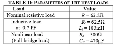
The power switches of the BHFL inverter are driven by three gate control signals, namely vpwm, vs and vu. The
timing diagram of these control signals is shown in Fig. 3. These control signals will then go through a series of logic gates shown in Fig. 4, and become the gating signal for each power switch. Referring to Fig. 3, vpwm is a
rectified sinusoidal pulse width modulated (SPWM)
pulse-train, and vs is a square-wave signal with frequency
half of vpwm. The unfolding signal, vu is a 50Hz sign
waveform. In Fig. 4, it can be seen that the resulting signals of logical operations between vpwm and vs are used
to drive the power switches of the high-frequency PWM bridge. Note that vs is used to alternatively split the
rectified SPWM pulses. On the transformer secondary side, vs is used to drive the power switches of the active
rectifier. The power switches of the polarity-reversing bridge are driven by vu.
B. Plant Modeling
To design a closed-loop controller for the BHFL inverter, the plant is first modeled using the state-space averaging technique [17]. Referring to Fig. 1, it is assumed that the dc source voltage, Vdc is constant. The
inverter switching frequency is considered to be high enough compared to the 50Hz sinusoidal modulating frequency. The high-frequency transformer is assumed to be operating in the linear area. As such, the high-frequency PWM bridge and the transformer can be modeled as constant gains. The polarity-reversing bridge is only operated at line-frequency (50Hz), thus its dynamics can be ignored. With these assumptions, the dynamics of the system can be simplified to a LC low-pass filter connected to the load. Choosing the filter inductor current iL and filter capacitor voltage vrect as the
state variables, the state-space representation and output equation of the system are derived:
or rect
L rect
L
i C u L v
i C
L dt
dv dt di
1 0
0 1
0 1
1 0
− + +
− =
(1)
[
]
=
rect L or
v i
v 0 1 (2) Based on (1) and (2), the system dynamic model is represented by the block diagram in Fig. 5. It can be seen that the load current acts as a disturbance on the output voltage, while the output voltage acts as a disturbance on the inductor current.
Since the controller is to be implemented using a digital processor, the dynamic model of the system is discretized. With a sampling period of Ts, the discrete-time
state-space equations can be written as:
)
(
)
(
)
(
)
1
(
k
Ax
k
Bu
k
B
i
k
x
+
=
+
+
d or (3)) ( )
(k Cx k
vor = (4) where
− =
=
) cos( ) sin( 1
) sin( 1 ) cos(
22 21
12 11
s s
s s
T T
C
T L T
A A
A A A
ω ω
ω
ω ω ω
− = =
) cos( 1
) sin( 1
2 1
s s
T T L B B B
ω ω
ω
−
− = =
) sin( 1
) cos( 1
2 1
s s
d d
d T
C T B
B B
ω ω
ω
[
0 1]
=
= ) ( ) ( ) ( k v k i k x rect
L is the state vector, and
LC
1
=
ω is the
cut-off frequency of the low-pass filter.
From (3) and (4), the discrete-time equations can be rewritten: ) ( ) ( ) ( ) 1 ( 1 ) ( 1 1 1 12 1 11 1 k i B B k v B A k i B A k i B k u or d or L
L + − − −
= (5)
) ( ) ( ) ( ) 1 ( 1 ) ( 21 2 21 2 21 22 21 k i A B k u A B k v A A k v A k i or d or or
L = + − − −
(6) From (5) and (6), it can be seen that additional disturbance terms appear because of model discretization. As compared to the continuous-time model, there exist two disturbances instead of one, acting on the inductor current and output voltage. The current and voltage disturbance terms can be written as:
) ( ) ( ) ( 1 1 1 12 k i B B k v B A k i or d or
d =− − (7) ) ( ) ( ) ( 21 2 21 2 k i A B k u A B k v or d
d =− − (8)
Based on the discrete-time equations, the digital model of the system can be represented by the block diagram in Fig. 6, where
z
−1 denotes a unit delay.III. CONTROLLER DESIGN
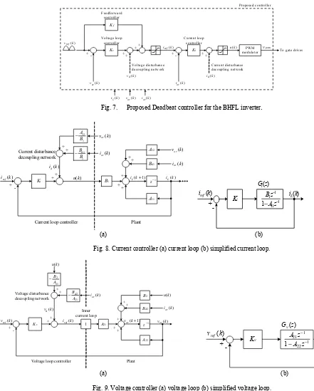
Fig. 7 shows the proposed Deadbeat controller for the BHFL inverter. It consists of inner current loop controller, outer voltage loop controller and a feed-forward controller. The feed-forward controller, which imposes a gain scheduling effect according to the reference signal, is used to compensate the steady-state error of the system. From the discrete-time model of the plant in Fig. 6, it is known that there are disturbance terms acting on the inductor current and output voltage. These disturbances are compensated using additional decoupling networks in (7) and (8). With that, the Deadbeat controller has good disturbance rejection capability and improved robustness towards load variations.
A. Current Loop Controller
Fig. 8(a) shows the inner current loop controller. The current disturbance decoupling network is added to compensate the disturbances acting on the inductor current. Canceling the current disturbance coupling allows a simple gain, Ki to be applied in forming the inner current loop. Referring to Fig. 8(a), the current loop control law can be derived:
u(k)=Ki
[
iref(k)−iL(k)]
+id(k) (9) whereu
(
k
)
is the control signal applied to the PWM modulator,i
ref(
k
)
is the inductor current reference generated by the outer voltage loop, andi
d(
k
)
is the current disturbance decoupling network from (7). Fig. 8(b) shows the simplified current loop. The discrete-time open-loop transfer function is:1 11 1 1 1 ) ( − − − = z A z B z Gi
[
1]
1 ) cos( 1 ) sin( − − − = z T L z T s s ω ω
ω (10)
The corresponding discrete-time closed-loop transfer function of the current loop is:
) ( 1 ) ( ) ( ) ( ) ( z G K z G K k i k i z C i i i i ref L i + = =
[
]
1 111 1 1 1 + − = − − z A B K z B K i i
[
K T L T]
z Lz T K s s i s i ω ω ω ω ω + − = − − 1 1 ) cos( ) sin( )
sin( (11)
From (11), the characteristic equation of the closed-loop current controller can be written as:
[
11− 1]
=0− A K B
z i cos( ) 1 sin( ) =0
−
− s i Ts
L K T
z ω
ω
ω (12)
In discrete-time control systems, the closed-loop poles or the roots of the characteristic equation must lie within the unit circle in z-plane for the system to be stable [10]. Therefore, the range of Ki for the system to be stable is:
[
]
11< 11− 1 <
− A KiB ,
1 11
1
11 1 1
B A K B A i + < <
− and
[
]
[
]
) sin( 1 ) cos( ) sin( 1 ) cos( s s i s s T T L K T T L ω ω ω ω ω ω + < <− (13)
To achieve Deadbeat response, the root is to be placed at the origin of the z-plane (
z
=
0
). Hence, the current loop gain, Ki is designed as:1 11
B A Ki =
) sin( ) cos( s s T T L ω ω ω
= (14) Substituting (14) into (11) yields:
) ( )
(k A11z 1i k
iL = − ref =cos(ωTs)z−1iref(k) (15) When ωTs is sufficiently small, sin(ωTs)≈ωTs and
1 )
cos(ωTs ≈ . Therefore, (15) can be written as )
( )
(k z 1i k
iL = − ref , which is the Deadbeat response.
B. Voltage Loop Controller
Fig. 9(a) shows the outer voltage loop controller. The voltage disturbance decoupling network is added to compensate the disturbances acting on the output voltage. This will improve the robustness of the system towards load variations, enabling various types of loads to be connected. Besides, it also acts as an additional current loop command to produce the needed load current without waiting for errors in voltage to occur.
The design procedure of the voltage loop controller is similar to the current loop controller. The voltage loop gain, Kv is applied to achieve Deadbeat response. From
Fig. 9(a), the voltage loop control law is derived:
[
( ) ( )]
( ))
(k K v k v k v k
iref = v ref − or + d (16) where
i
ref(
k
)
is the generated current loop command for the inner current loop,v
ref(
k
)
is the rectified sinusoidal voltage reference, andv
d(
k
)
is the voltage disturbance decoupling network from (8). Fig. 9(b) shows the simplified voltage loop. It can be noted that the inner current loop is viewed as a constant gain, with the condition of current loop is well designed. The corresponding discrete-time open-loop transfer function is:1 22 1 21 1 ) ( − − − = z A z A z Gv
[
1]
1 ) cos( 1 ) sin( − − − = z T C z T s s ω ω
ω (17)
The discrete-time closed-loop transfer function of the voltage loop is:
) ( 1 ) ( ) ( ) ( ) ( z G K z G K k v k v z C v v v v ref or v + = =
[
21 22]
1 11 21 + − = − − z A A K z A K v v
[
K T C T]
z Cz T K s s v s v ω ω ω ω ω + − = − − 1 1 ) cos( ) sin( )
sin( (18)
From (18), the characteristic equation of the closed-loop voltage controller can be written as:
[
22 − 21]
=0− A K A
z v , 1 sin( ) 0
) cos( = −
− s v Ts
C K T
z ω
ω
ω (19)
For the system to be stable, the range of Kv is:
[
]
11< 22− 21 <
− A KvA ,
21 22 21
22 1 1
A A K A A v + < < −
[
]
[
]
) sin( 1 ) cos( ) sin( 1 ) cos( s s v s s T T C K T T C ω ω ω ω ω ω + < <− (20)
Similar to the current loop gain, the voltage loop gain, Kv
is designed such that the root of the system can be placed at the origin of z-plane:
21 22
A A Kv =
) sin( ) cos( s s T T C ω ω ω
= (21) Substituting (21) into (18) yields:
) ( )
(k A22z 1v k
vor ref
−
= cos( Ts)z 1vref(k)
−
= ω (22) When ωTs is sufficiently small, sin(ωTs)≈ωTs and
1 )
cos(ωTs ≈ . Therefore, (22) can be written as
) ( )
(k z 1v k
vor ref
−
= , which is the deadbeat response. C. Feed-forward Controller
From (22), it can be seen that there is a steady-state error in the output voltage if
ω
T
s is not sufficiently small. To compensate the steady-state error, a feed forward controller is added to the output of the voltage loop controller. The feed forward controller imposes a gain scheduling effect on the voltage loop controller according to the reference signal. The voltage loop with inclusion of feed forward controller is shown in Fig. 10 and the discrete-time closed-loop transfer function is derived:[
]
[ ] 1
) ( ) ( 1 22 21 1 21 + − + = − − z A A K z A K K k v k v v f v ref
or
[
]
[K T C T ]z C
z T K K s s v s f v ω ω ω ω ω + − + = − − 1 1 ) cos( ) sin( )
sin( (23)
To ensure Deadbeat response, the feed forward gain, Kf is
chosen as: 21 22 1 A A Kf − = [ ] ) sin( ) cos( 1 s s T T C ω ω ω −
= (24)
Substituting (21) and (24) into (23), vor(k) z 1vref(k)
−
=
is obtained, which ensures the Deadbeat response.
IV. HARDWARE REALIZATION AND PRACTICAL ISSUES
A 1kVA prototype inverter has been constructed. The proposed Deadbeat controller is implemented using the DS1104 digital signal processor (DSP) from dSPACE (64-bit floating-point processor with TMS320F240 Slave DSP). Hall-effect current sensors, HY10-P and voltage
sensor, LV25-P are used to sense the feedback signals. The signal conditioning such as noise filtering and signal amplification are performed in software using the DS1104 DSP. Table I provides the parameters of the prototype inverter.
TABLEI:PARAMETERS OF THE PROTOTYPE INVERTER
Parameter Value
Switching frequency fsw = 25kHz
Nominal input voltage Vdc = 150V
Rated output voltage vo = 240Vrms
Rated output frequency f = 50Hz
Rated output power Po = 1kVA
Filter inductor L = 0.66mH
Filter capacitor C = 6.8µF
Sampling period Ts = 40µs
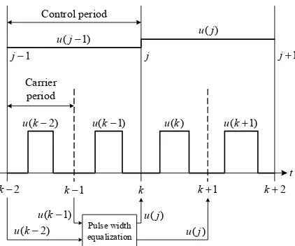
In practice, the pulse width of kth pulse and (k+1)th pulse are not equal in vHF due to the SPWM switching, as
shown in Fig. 11. This results in a low-frequency voltage envelope to exist over the entire waveform. The low-frequency voltage envelope may lead to possible transformer saturation, as the transformer is designed for high frequency operation. To overcome this problem, an equalized pulse PWM technique is proposed, where the pulse width of the kth pulse is equalized to the (k+1)th pulse. Through this approach, the use of dc blocking capacitor at the primary side of transformer [18] is avoided. Fig. 12 illustrates the timing diagram of the equalized pulse PWM generation. The equalized pulse is calculated using the following equation:
2 ) 1 ( ) 2 ( )
(j =u k− +uk−
u (25) where j denotes the number of control period sample, and
k denotes the number of carrier period sample. Note that the real-time application of the proposed control algorithm including this equalized pulse PWM technique is implemented using a single timer. The equalized pulse is updated once in two carrier periods, where the carrier period equals to the defined timer period.
V. EXPERIMENTAL RESULTS AND DISCUSSION
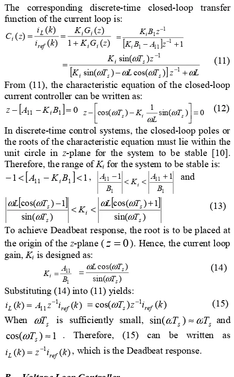
To verify the performances of the proposed deadbeat controller, the prototype inverter has been tested under various types of loads. Besides the resistive and inductive loads, the system is also tested under phase controlled triac load and full-bridge rectifier load. The parameters of the test loads are summarized in Table II.
TABLEII:PARAMETERS OF THE TEST LOADS
Load Value
Nominal resistive load R = 62.5Ω
Inductive load at 0.7 PF
Ri = 62.5Ω
Li = 183mH
Nonlinear load (Full-bridge load)
Rd = 500Ω
Cd = 470µF
The output voltage and current waveforms under resistive load are shown in Fig. 13. The output voltage total harmonic distortion (THD) is 1.5%. The output voltage and current waveforms under inductive load are
shown in Fig. 14. It can be seen that the system is capable of carrying bidirectional power flow. The output voltage THD under this condition is 2.2%.
Fig. 15 shows the output voltage and current waveforms under triac load commutated at 90o/270o. It is observed that the voltage drop can be recovered quickly after the large current transient. The voltage transient is reduced to 10% in 0.32ms.
To test a worst case loading, the system is connected to a full-bridge rectifier. This type of load is considered to be the most severe type. It causes intense voltage distortion due to the highly distorted current. Fig. 16 shows the steady-state output voltage and current waveforms under full-bridge rectifier load. As can be seen, the output voltage waveform has good quality with low distortion. The output voltage THD under this condition is 3.8%. This can be attributed to the improved robustness of the system.
VI. CONCLUSIONS
A deadbeat controller for closed-loop regulation of the BHFL inverter has been described in this paper. The proposed control scheme regulates both the output voltage and inductor current using the multicolor control strategy. A feed-forward controller is incorporated to compensate steady-state error of the system. Accurate disturbance decoupling makes the system capable of handling various types of loads. An equalized pulse PWM technique has also been introduced to avoid transformer saturation caused by low frequency voltage envelopes. The proposed controller, including the pulse equalization and signal conditioning, have been realized in DS1104 DSP using a single timer. The laboratory experiments on a 1kVA prototype inverter verified the proposed control strategy. The experimental results show that the controller exhibits very fast dynamic response under cyclic step load changes. Besides, a sinusoidal voltage waveform with low distortion can be maintained even under highly nonlinear loads. The closed-loop BHFL inverter is thus suitable for wide area of applications, both in grid-connected and stand-alone configurations.
REFERENCES
[1] M. J. Ryan and R. D. Lorenz, “A high performance sine wave inverter controller with capacitor current feedback and ‘back-EMF’ decoupling,” IEEE PESC Conf. Rec.,
June 1995, Atlanta, Georgia, pp. 507-513.
[2] N. M. Abdel-Rahim and J. E. Quaicoe, “Analysis and design of a multiple feedback loop control strategy for single-phase voltage-source UPS inverters,” IEEE Trans. Power Electron., vol. 11, no. 4, pp. 532-541, July 1996.
[3] S. Choudhury, “Implementing triple conversion single-phase on-line UPS using TMS320C240,” Application Report SPRA589A, Texas Instruments, 1999.
[4] S. L. Jung and Y. Y. Tzou, “Sliding mode control of a closed-loop regulated PWM inverter under large load variations,” IEEE PESC Conf. Rec., June 1993, Seattle, Washington, pp.507-513.
[5] T. L. Tai and J. S. Chen, “UPS inverter design using discrete-time sliding mode control scheme,” IEEE Trans. Ind. Electron., vol. 49, no. 1, pp. 67-75, Feb. 2002.
[6] T. Haneyoshi, A. Kawamura and R. G. Hoft,
“Waveform compensation of PWM inverter with cyclic fluctuating loads,” IEEE Trans. Ind. Applicat., vol. 24, no. 4, pp. 582-589, July/Aug. 1988.
[7] S. C. Yeh and Y. Y. Tzou, “Adaptive repetitive control of a PWM inverter for ac voltage regulation with low harmonic distortion,” IEEE PESC Conf. Rec., June 1995, Atlanta, Georgia, pp. 157-163.
[8] T. F. Wu, C. H. Yang, Y. K. Chen and Z. R. Liu, “Photovoltaic inverter systems with self-tuning fuzzy control based on an experimental planning method,”
IEEE IAS Annu. Meeting Conf. Rec., Oct. 1999, Phoenix, Arizona, pp. 1887-1894.
[9] X. Sun, D. H. Xu, F. H. F. Leung, Y. S. Wang and Y. S. Lee, “Design and implementation of a neural-network-controlled UPS inverter,” IEEE IECON Conf. Rec.,
Nov./Dec. 1999, San Jose, California, pp. 779-784. [10] K. Ogata, Discrete-Time Control Systems. 2nd ed. New
Jersey: Prentice Hall, 1995, pp.416-417/pp. 182-183. [11] K. P. Gokhale, A. Kawamura and R. G Hoft, “Deadbeat
microprocessor control of PWM inverter for sinusoidal output waveform synthesis,” IEEE Trans. Ind. Appicat.,
vol. IA-23, no. 5, pp. 901-910, Sept./Oct. 1987.
[12] A. Kawamura, T. Haneyoshi and R. G. Hoft, “Deadbeat controlled PWM inverter with parameter estimation using only voltage sensor,” IEEE Trans. Power Electron., vol. 3, no. 2, pp. 118-125, Apr. 1988.
[13] C. C. Hua, “High switching frequency DSP controlled PWM inverter,” IEEE Contr. Applicat. Conf. Rec., Sept. 1993, Vancouver, British Columbia, pp. 273-283. [14] S. L. Jung, M. Y. Chang, J. Y. Jyang, L. C. Yeh and Y.
Y. Tzou, “Design and implementation of an FPGA-based control IC for ac-voltage regulation,” IEEE Trans. Power Electron., vol. 14, no. 3, pp. 522-532, May 1999. [15] L. Mihalache, “DSP control method of single-phase
inverters for UPS applications,” IEEE APEC Conf. Rec.,
Mar. 2002, Dallas, Texas, pp. 590-596.
[16] M. Z. Ramli, Z. Salam, L. S. Toh and C. L. Nge, “A bidirectional high-frequency link inverter using center-tapped transformer,” IEEE PESC Conf. Rec., June 2004, Aachen, Germany, pp. 3883-3888.
[17] N. Mohan, T. M. Undeland and W. P. Robbins, Power Electronics: Converter, Applications and Design. 3rd ed. New Jersey: John Wiley and Sons, 2003, pp. 323-328. [18] E. Koutroulis, J. Chatzakis, K. Kalaitzakis, and N. C.
Voulgaris, “A bidirectional, sinusoidal, high-frequency inverter design,” IEE Proc. Elect. Power Applicat., vol. 148, no. 4, pp. 315-321, July 2001.
Vdc
Center-tapped high-frequency transformer High-frequency
PWM bridge
vHF
Active rectifier
vpwm_rect
Polarity-reversing bridge Low-pass
filter
+
-io
vo L
C Load
idc
S1
S1 S2
S2
S4
S4 S5
S5 +
-vrect
+
-S3
S3 +
-N1:N2
Fig. 1. Bidirectional high-frequency (BHFL) inverter.
vHF
t
vpwm_rect
t
1 2 Vdc
N N
t vrect
vo
t
Vdc
vpwm
t vs
vu
t t
Fig. 2. Key waveforms at the principal conversion stages. Fig. 3. Gate control signals for the BHFL inverter.
Gate Drive
Gate Drive
Gate Drive
Gate Drive
Gate Drive
Gate Drive
Gate Drive
Gate Drive
Gate Drive
Gate Drive
vpwm
vs
vu
1 S
2 S
2 S
3 S
3 S
4 S
4 S
5 S
5 S
1 S
u
+
- sC
1
sL
1
) ( 1
s Z
vor
ic
iL
ior
+
-Unknown load
Fig. 4. Interface between control signals and power switches. Fig. 5. Continuous-time model of the BHFL inverter.
+
1 −
z B1
+ +
A21
+
1 −
z
A22
+ +
A11
) (k
u iL(k+1) iL(k) vor(k+1) vor(k)
Bd1
A12
+ +
) (k vor
) (k ior
B2
+ +
) (k u
) (k ior Bd2
Fig. 6. Discrete-time model of the BHFL inverter.
Fig. 7. Proposed Deadbeat controller for the BHFL inverter
.
+
1
−
z B1
+ +
A11
) (k
u iL(k+1) iL(k)
Bd1 A12
+ +
) (k vor
) (k ior
Ki
+ +
) (k vor
) (k ior
1 12
B A
−
1 1
B Bd
−
) (k id
++ )
(k iref
+
-Current disturbance decoupling network
Current loop controller Plant
+
-Ki
) (k iref
1 11
1 1
1 −
−
−Az z
B iL(k) )
(z Gi
(a) (b)
Fig. 8. Current controller (a) current loop (b) simplified current loop.
+
1 −
z
+ +
A22 ) 1 (k+
vor vor(k)
Bd2
B2 +
+
) (k ior
Kv
+ + ) (k u
) (k ior
21 2
A Bd
−
) (k vd
++ )
(k vref
+
-Voltage disturbance decoupling network
Voltage loop controller Plant Inner
current loop 21
2
A B −
) (k u
A21 )
(k iref
1
+
-Kv
) (k
vref vor(k)
) (z Gv
1 22
1 21
1 −
−
−A z z A
(a) (b)
Fig. 9. Voltage controller (a) voltage loop (b) simplified voltage loop.
+
-Kv
) (k
vref vor(k)
) (z Gv
1 22
1 21
1 −
−
−A z z A Kf
+ +
Fig. 10. Voltage loop with feed forward controller. Fig. 11. Timing diagram of vHF without pulse equalization.
vHF t
) 1 ( ) (k =u k+ u
) 1 (k+ u
) (k u
Kv Voltage loop
controller
Ki PWM
modulator To gate drives
vpwm
+
Voltage disturbance decoupling netw ork
Proposed controller
-) (k vref
) (k vd )
(k vor
Kf Feedforward
controller
) (k iref
+
-) (k ior
) (k id
+ +
+ +
+ +
Current loop controller
Current disturbance decoupling network
) (k u
) (k vor ior(k) )
(k iL
t
) (k
u u(k+1)
) 1 (k−
u
) 2 (k−
u
k k+1 k+2
1
−
k
2
−
k
Pulse width equalization
) 1 (k−
u
) 2 (k−
u
Carrier period
j j+1
1
−
j
) 1 (j−
u u(j)
Control period
) (j u
) (j u
Fig. 12. Timing diagram of equalized pulse PWM generation.
Fig. 13. Output voltage and current for resistiveload.
Fig. 14. Output voltage and current for inductive load. Vertical scale: output voltage 100V/div, Vertical scale: output voltage 100V/div, output current 5A/div, Time scale: 4ms/div output current 2A/div, Time scale: 4ms/div
Fig. 15. Output voltage and current for triac load. Fig. 16. Output voltage and current for rectifier load. Vertical scale: output voltage 100V/div, Vertical scale: output voltage 100V/div,
output current 5A/div, Time scale: 2ms/div output current 5A/div, Time scale: 4ms/div vo
io vo
io vo
io
vo
io