NBTI degradation effect on advanced-process 45 nm high-
k
PMOSFETs
with geometric and process variations
S.F. Wan Muhamad Hatta
a,*, N. Soin
a, D. Abd Hadi
a, J.F. Zhang
b aDepartment of Electrical Engineering, University of Malaya, 50603, MalaysiabSchool of Engineering, Liverpool John Moores University, L3 3AF, United Kingdom
a r t i c l e
i n f o
Article history: Received 1 July 2010 Accepted 8 July 2010 Available online 4 August 2010
a b s t r a c t
Negative bias temperature instability (NBTI) has become an important reliability concern for nano-scaled complementary metal oxide (CMOS) devices. This paper presents the effect of NBTI for a 45 nm advanced-process high-kdielectric with metal gate PMOS transistor. The device had incorporated advanced-process flow steps such as stress engineering and laser annealing in order to achieve high on-state drain current drive performance. To explore NBTI effects on an advanced-process sub-micron device, the 45 nm high-k PMOS transistor was simulated extensively with a wide range of geometric and process variations. The device was simulated at varying thicknesses in the dielectric layer, oxide interfacial layer, metal gate and polysilicon layer. In order to observe the NBTI effect on process variation, the NBTI degradation of the 45 nm advanced-process PMOS is compared with a 45 nm PMOS device which does not employ pro-cess-induced stress and incorporates the conventional rapid thermal annealing (RTA) as compared to the laser annealing process which is integrated in the advanced-process device flow. The simulation results show increasing degradation trend in terms of the drain current and threshold voltage shift when the thicknesses of the dielectric layer, oxide layer as well as the metal gate are increased.
Ó2010 Elsevier Ltd. All rights reserved.
1. Introduction
Deep-sub-micron device scaling is a phenomenon which is rap-idly evolving for ultra-scaled MOSFETs and the design of this tech-nology requires stringent control of short-channel effects (SCE) and sub-threshold behavior. With this in mind, the gate dielectrics should be thinned to less than 1.0–1.5 nm equivalent oxide thick-ness (EOT)[1]. It has been reported that due to quantum mechan-ical tunnelling, the typmechan-ical leakage current of SiO2at gate voltage,
Vg of 1 V can change from 1012A/cm2 with EOT of 3.5 nm to 10 A/cm2with EOT of 1.5 nm[2]. To achieve the EOT target stated above and to counter the issue of leakage currents, dielectric mate-rials with higher permittivity, k values as compared to SiO2 (k> 3.9) are introduced. Compounds of hafnium (Hf), zirconium (Zr), and aluminium (Al) have been proposed as potential high-k
dielectric materials and hafnium oxide (HfO2) has emerged as a promising gate dielectric to replace the conventional SiO2due its high dielectric constant (k= 25), wide bandgap (E0= 5.7 eV)[3], acceptable band offset with respect to silicon (DEc= 1.5 eV)[3], and process conditions which are compatible with silicon process flow integration. An ultimate reliability issue in sub-micron CMOS devices is the negative bias temperature instability (NBTI) phe-nomenon. Transistors tend to exhibit changes in transistor
charac-teristics over time such as shifts in threshold voltage (D|Vth|), as well as significant changes in drain current (ID) and transconduc-tance (Gm). This phenomenon is due to the creation of interface states (Nit) and oxide trapped charged (Not) whereby the mecha-nism is accelerated by negative bias and elevated temperature. This paper presents the NBTI degradation effect on advanced-pro-cess 45 nm PMOS device in which transistor parameters such as the drain current and threshold voltage shifts will be observed con-sequent to the application of stress temperature. This work will look into the variation of each stack layer of the device and the influences of each stack layer to the NBTI effect.
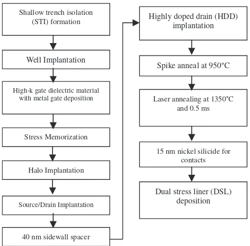
2. Methodology of advanced-process 45 nm PMOS device
An advanced- process sub-micron technology device incorpo-rates advanced process steps in order to overcome process-related challenges such as ultra-shallow junction (USJ) formation, reduc-tion in current leakage, suppressing transient-enhanced diffusion and achieving device’s performance targets, such as the on- and off- current targets, while controlling short-channel effects. A dis-tinct procedure which promotes advanced-process technology is the millisecond laser annealing for ultra-shallow junction forma-tion. This procedure replaces the conventional procedures of ion implantation and subsequent rapid thermal annealing, in forming the doped region of a sub-micron transistor. The process flow of
0026-2714/$ - see front matterÓ2010 Elsevier Ltd. All rights reserved. doi:10.1016/j.microrel.2010.07.022
* Corresponding author. Tel.: +60 176119960; fax: +60 379675316. E-mail address:[email protected](S.F. Wan Muhamad Hatta).
Contents lists available atScienceDirect
Microelectronics Reliability
a PMOS device consisting of an advanced-process flow is given in Fig. 1 [4].
2.1. Devices and simulation conditions
The device used in this simulation is a 45 nm hafnium-based dielectric combined with TiN metal gate PMOS transistor and its process steps reflects the standard manufacturing trends for a sub-micron device. The process flow of the simulated device is as presented in Fig. 1 whereby it adopts the deposition of high-k
dielectrics with metal gate, application of stress engineering as well as the adoption of laser annealing as compared to the conven-tional rapid thermal annealing. To further explore the NBTI effects on different structures of advanced high-k devices, the high-k
PMOS device was simulated extensively with a wide range of metric and process variations. NBTI was studied by varying geo-metric properties which are the thicknesses of the high-k
dielectric layer, oxide interfacial layer, TiN metal gate layer and polysilicon layer respectively. The varied geometric properties of the device are as presented inFig. 2. In regards to process varia-tions, the NBTI degradation of the device was studied by simulating and comparing devices with and without process-induced stress effects as well as comparing devices which are processed with the conventional RTA to the devices which are processed with both
RTA and laser annealing (LA). The technology CAD (TCAD) Sentau-rus Synopsys simulator tool was used to study the NBTI effects of these geometric and process variations.
3. Simulation results
The following subsections present the simulation results, which are the drain current degradation, the threshold voltage shifts and the interface trap concentration subsequent to bias temperature stress. The geometric properties of the advanced-process 45 nm device were extensively varied and the after-effects are presented in subsection3.1whereas subsection3.2presents the comparison of simulated results of the device which incorporates advanced process-induced stress and LA steps, compared to the device which follows the conventional process flow.
3.1. Geometric variation of device
The high-kPMOS device is varied in terms of the thicknesses of the high-kdielectric layer, oxide interfacial layer, metal gate layer and polysilicon layer. NBTI effect is observed by analysing the drain current degradation, threshold voltage shifts and interface trap concentration when the device is stressed at stress temperatures ranging from 300 K to 400 K, as had been carried out in most experimental works[5]. For the simulation of each varied device parameters, the unvaried parameter thicknesses were set to the standard sub-micron device specification highlighted in[6].
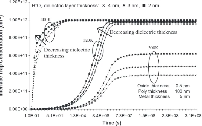
3.1.1. Influence of high-k dielectric thickness on NBTI
When biased at room temperature of 300 K, the drain current degradation is found to be significant as the dielectric thickness is decreased. However, it is observed that at a higher stress tem-perature of 400 K, the drain current degradation becomes more significant as the thickness of the HfO2dielectric layer is increased. This is in agreement to the single-pulse measurement carried out by[7]which had also obtained a current degradation of around
300
lA/lm for the similar range of gate biases and HfO
2thick-nesses which were used in this current work. From Eqs. (1) and (2) below, it is shown that the oxide thickness is inversely propor-tional to the drain current and thus it is in agreement with the graph inFig. 3for the HfO2dielectric thickness variation[8]. As the dielectric thickness increases, the drain current would be fur-ther reduced leading to higher drain current degradation.
ID¼
l
CoxWLaser annealing at 1350 C and 0.5 ms
15 nm nickel silicide for contacts
Dual stress liner (DSL) deposition
Fig. 1.Process flow of the simulated advanced-process 45 nm high-k PMOS transistor.
The uppermost right hand side ofFig. 3presents the threshold voltage shift versus HfO2dielectric thickness. It is observed that the threshold voltage increases in proportion with the HfO2 dielec-tric thickness and this can be described from Eqs. (2) and (3)[8] where the threshold voltage is proportional with oxide thickness. The device with thinner HfO2layer exhibits less threshold voltage shift. This is due to less charge trapping/de-trapping at pre-existing defects in the bulk high-klayer[9].Fig. 4presents the interface trap concentration (Nit) as a function of stress time (t) with a var-iation of HfO2 dielectric thicknesses and temperature. From this figure, it is shown thatNitincreases as the temperature is increased for all three different HfO2dielectric thicknesses. For every applied stress temperature, it shows that the Nit increases as the HfO2 dielectric thickness is decreased. This behavior is in agreement with a review paper done by Ribes et al.[10]in which he stated that the NBTI degradation is due to holes trap (metastable states) which recovers and interface state which are stable and does not recover. It is also observed that the devices stressed at higher stress temperature tend to reach steady-state occupation at an earlier time.
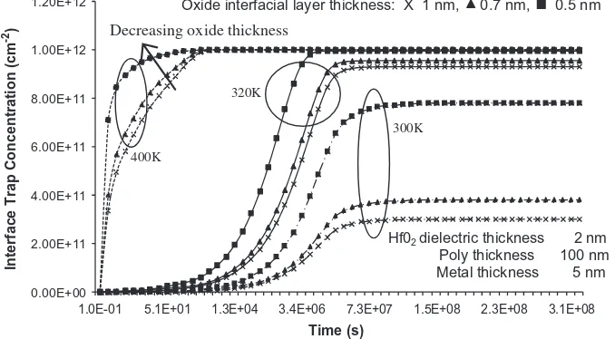
3.1.2. Influence of oxide interfacial layer thickness on NBTI
The introduction of the HfO2gate stack would consists of two layers which are the HfO2film and a thin 0.5- to 1.5-nm SiO2 inter-facial layer (IL)[11]. This interfacial layer is grown either intention-ally or spontaneously in the Si surface as a consequence of when the Hf-based dielectric is deposited onto the silicon. In this section the oxide interface layer thickness had been varied (1 nm, 0.7 nm, 0.5 nm) and the drain current versus gate voltage (IDVG) charac-teristic along with the threshold voltage and interface trap concen-tration shifts were analysed. The oxide interface layer variation observed inFig. 5shows anIDVGtrend which is similar to that described in the previous section. The threshold voltage shift also exhibits a similar behavior as in the previous section whereby the threshold increases with the oxide thickness increment. The interface trap concentration increases as the oxide interfacial layer thickness decreases as shown inFig. 6and the trend is similar as in the previous section. Devices with thinner gate oxide would expe-rience a higher gate oxide electric field and this vertical electric field tends to accelerate the NBTI effect by increasing the speed of the diffusing hydrogen species, thus generating interface traps. 0
0.000005 0.00001 0.000015 0.00002 0.000025 0.00003 0.000035 0.00004
-1.2 -1.08 -0.96 -0.84 -0.72 -0.6 -0.48 -0.36 -0.24 -0.12 0
Drain Current Degradation (A/um)
Gate Voltage (V) Increasing dielectric
Decreasing dielectric thickness
HfO2 dielectric layer thickness:
X 4 nm, 3 nm, 2 nm
400 K 320 K 300 K
Oxide thickness 0.5 nm Poly thickness 100 nm Metal thickness 5 nm
0 5 10 15 20 25 30 35 40 45
1nm 2nm 3nm 4nm
Δ
Threshold Voltage (mV)
HfO2 Layer Thickness
400K
300K 320K
400K
320K
300K
Fig. 3.Drain current degradation of a 45 nm high-kPMOS stressed at temperatures 300–400 K. The high-kdielectric layer thickness had been varied from 2 nm to 4 nm. Inset caption is the threshold voltage shift of when the HfO2layer thickness is varied from 1 nm to 4 nm.
0.00E+00 2.00E+11 4.00E+11 6.00E+11 8.00E+11 1.00E+12 1.20E+12
1.0E-01 5.1E+01 1.3E+04 3.4E+06 7.3E+07 1.5E+08 2.3E+08 3.1E+08
Interface Trap Concentration (cm
-2)
Time (s)
300K
Decreasing dielectric thickness
HfO2 dielectric layer thickness: X 4 nm, 3 nm, 2 nm
Oxide thickness 0.5 nm Poly thickness 100 nm Metal thickness 5 nm
Decreasing dielectric
thickness
320K 400K
Fig. 4.Interface trap concentration for various thicknesses of the HfO2dielectric layer subsequent to bias temperature stress.
It is observed that the slope of the trap density is steeper for the device with thinner oxide layer which indicates higher contribu-tion of the interface charges. This phenomenon is verified through experimental studies carried out by[12–14].
3.1.3. Influence of metal gate thickness on NBTI
In this work, the metal gate TiN is used as a capping layer before the polysilicon deposition and the influence it imposed to the ef-fect of NBTI is studied by varying its thickness from 3 nm (thin TiN) to 10 nm (thick TiN). It can be observed inFigs. 7 and 8that at high stress temperature of 400 K, the NBTI degradation becomes more significant as the thickness of the TiN metal gate layer in-creases. Similar to the cases of when the thickness of the high-k
dielectric and the SiO2interfacial layer were varied, it is observed that the drain current degradation increases as the thickness of the layer is increased. However in terms of the interface trap con-centrationDNit, the trap density is observed to increase as the me-tal gate thickness layer is increase. This is in agreement with the experimental work carried out by[15]where it had been deduced that by reducing the metal gate thickness, the mobility degradation
and NBTI effect are significantly reduced. The observation on the interface trap density characteristic is in reverse when compared to the effects imposed when varying the thicknesses of the HfO2 dielectric and SiO2 interfacial layers. It is also observed that the DNit arrives at the same level of steady-state occupation, when the device is stressed at 320 K and 400 K.
A charge pumping technique and pulsedIdVgmeasurement had been carried out by[16]to analyse the reliability of a device with a variation of the metal gate thickness. In agreement to the current work, thicker TiN results in higher interface trap concen-tration. It had been found that for thick TiN metal gates, high inter-face density at high stress temperatures was evident due to stress from the metal nitride layer. This stress is as a result of the agglom-eration effect which evolves from the growing of the crystallites of TiN films which in turn causing elastic deformation and thus caus-ing stress in the TiN metal layer. The increascaus-ing of the TiN gate thickness results in the increase of the nitrogen species diffusion towards the Si interface which enhances degradation. The mecha-nism of this effect is as follows; when the nitrogen species diffuses towards the Si02/Si interface, the carrier mobility is degraded by 0
0.000005 0.00001 0.000015 0.00002 0.000025 0.00003 0.000035 0.00004
-1.2 -1.08 -0.96 -0.84 -0.72 -0.6 -0.48 -0.36 -0.24 -0.12 0
Drain Current Degradation (A/um)
Gate Voltage (V)
Oxide thickness: X 1 nm, 0.7 nm, 0.5 nm
400 K
320 K
300 K
300K 320K 400K
HfO2 thickness 2 nm Poly thickness 100 nm Metal thickness 5 nm
0 10 20 30 40 50 60
0.5nm 0.7nm 1nm
Threshold Voltage (mV)
Oxide Thickness
320K
400K
Increasing IL thickness
Decreasing IL thickness
300K
Δ
Fig. 5.Drain current degradation of a 45 nm high-kPMOS stressed at temperatures 300–400 K. The interface layer (IL) thickness had been varied at 0.5–1 nm. Inset caption is the threshold voltage shift of when the oxide thickness is varied at 0.5–1 nm.
0.00E+00 2.00E+11 4.00E+11 6.00E+11 8.00E+11 1.00E+12 1.20E+12
1.0E-01 5.1E+01 1.3E+04 3.4E+06 7.3E+07 1.5E+08 2.3E+08 3.1E+08
Interface Trap Concentration (cm
-2)
Time (s)
300K
Decreasing oxide thickness
320K
400K
Oxide interfacial layer thickness: X 1 nm, 0.7 nm, 0.5 nm
Hf02 dielectric thickness 2 nm
Poly thickness 100 nm Metal thickness 5 nm
0 0.000005
0.00001 0.000015 0.00002 0.000025 0.00003
-1.2 -1.08 -0.96 -0.84 -0.72 -0.6 -0.48 -0.36 -0.24 -0.12 0
Drain Current Degradation (A/µm)
Gate Voltage (V)
Increasing metal gate thickness
Metal thickness: 10 nm 6 nm X 3 nm
400 K 320 K
HfO2 dielectric thickness 2 nm
Poly thickness 100 nm Oxide thickness 0.5 nm
10 12 14 16 18 20 22 24 26 28 30
5nm 4nm 3nm
Threshold Voltage
(mV)
Metal Gate Thickness 400K 320K 300K
Δ
Fig. 7.Drain current degradation of the 45 nm high-k PMOS stressed at temperatures 320 K and 400 K. The metal gate thickness had been varied at 3 nm, 6 nm and 10 nm.
0.00E+00 2.00E+11 4.00E+11 6.00E+11 8.00E+11 1.00E+12 1.20E+12
1.00E-01 5.11E+01 1.31E+04 3.36E+06 7.34E+07 1.53E+08 2.33E+08 3.13E+08
Interface Trap Concentration (cm
-2)
Time (s)
Metal thickness: 5 nm
3 nm
HfO2 dielectric thickness 2 nm Poly thickness 100 nm Oxide thickness 0.5 nm 400 K
Increasing metal
gate thickness
320 K
300 K
Fig. 8.Interface trap concentration of the 45 nm high-kPMOS stressed at temperatures 300 K, 320 K and 400 K. The metal gate thickness had been varied at 3 nm and 5 nm.
0 0.000005 0.00001 0.000015 0.00002 0.000025 0.00003
-1.2 -1.08 -0.96 -0.84 -0.72 -0.6 -0.48 -0.36 -0.24 -0.12 0
Drain Current Degradation (A/µm)
Gate Voltage (V)
Increasing polysilicon thickness
Polysilicon thickness:X 100 nm 80 nm 50 nm
400 K 320 K
HfO2 dielectric thickness 2 nm Metal thickness 5 nm Oxide thickness 0.5 nm
means of the coulomb-scattering mechanism. The degradation of the carrier mobility results in the hole trapping which governs the effect of NBTI. The inset figure inFig. 7shows the threshold voltage shifts for a variation of the TiN metal gate layer thickness. It can be observed that as the metal gate becomes thinner, the threshold voltage shift becomes more significant. Thinner TiN layer would result in lesser diffusion of nitrogen as described above and elaborated by[17]. This will lead to lower electronegativity[18]of the nitrogen atoms which in turn lowers the workfunction. Hence, as TiN becomes thinner, the threshold voltage of the device moves to a higher negative value and thus suggesting that the thinner TiN has a lower workfunction.
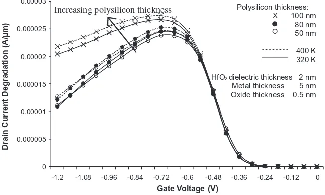
3.1.4. Influence of polysilicon thickness on NBTI
The polysilicon thickness in this work had been varied at 100 nm, 80 nm and 50 nm.Figs. 9 and 10show that the NBTI effect is increased as the polysilicon thickness is increased. The device with the polysilicon thickness of 100 nm exhibits a significant cur-rent degradation when it is biased at high negative voltage, irre-spective of the stress temperature. For thinner devices with
polysilicon thicknesses of 80 nm and 50 nm, the device degrada-tion is significant when biased at higher temperature, which is 400 K in this work. It is observed that as the polysilicon layer thick-ness is increased, the interface trap density increases. This may be due to the diffusion of Si from the polysilicon layer towards the high-kdielectric layer[19]. There are reports claiming that the de-vice should be built with a single metal electrode layer without the deposition of polysilicon on top[20]but this may result in stress-induced damage[21]. In order to improve the thermal stability of the electrode, the polysilicon/TiN stack is to be incorporated and the polysilicon layer thickness needs to be optimized in order to obtain better device reliability.
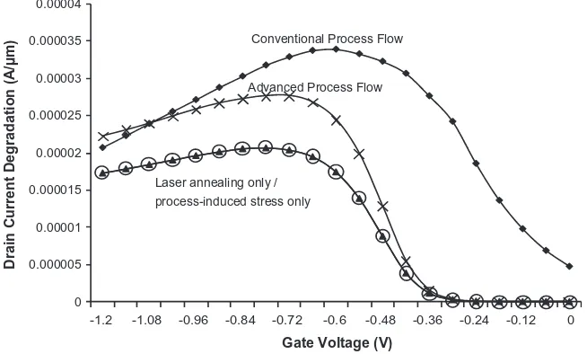
3.2. Process variation of device
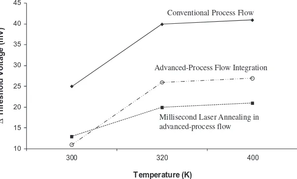
From theFig. 11, it is observed that the advanced-process flow, which incorporates millisecond laser annealing and process-in-duced stress, results in less drain current degradation as compared to the conventional process flow. The former process flow exhibits less amount of shift in the threshold voltage as the stress
temper-0.00E+00 2.00E+11 4.00E+11 6.00E+11 8.00E+11 1.00E+12 1.20E+12
1.00E-01 5.11E+01 1.31E+04 3.36E+06 7.34E+07 1.53E+08 2.33E+08 3.13E+08
Interface Trap Concentration (cm
-2)
Time (s)
Increasing polysilicon
thickness
400 K
320 K 300 K
Polysilicon thickness:
X 100 nm 80 nm 50 nm
HfO2 dielectric thickness 2 nm Metal thickness 5 nm Oxide thickness 0.5 nm
Fig. 10.Interface trap concentration of a 45 nm high-kPMOS stressed at temperatures 320 K and 400 K for a variation of polysilicon thickness.
0 0.000005 0.00001 0.000015 0.00002 0.000025 0.00003 0.000035 0.00004
-1.2 -1.08 -0.96 -0.84 -0.72 -0.6 -0.48 -0.36 -0.24 -0.12 0
Drain Current Degradation (A/µm)
Conventional Process Flow
Advanced Process Flow
Laser annealing only / process-induced stress only
Gate Voltage (V)
ature is increased, as shown inFig. 12. The incorporation of the millisecond laser annealing promotes device reliability due low interfacial state density[22]. It can be deduced that the incorpora-tion of millisecond laser annealing and process-induced stress fa-vours the reduction in the NBTI effect of the 45 nm high-kdevice.
4. Conclusions
This paper presents the NBTI degradation analysis on geometric and process variation on an advanced-process 45 nm PMOS device. The drain current degradation and threshold voltage shift were ob-served to increase considerably when the device is stressed at 400 K and the increase in degradation is more significant as the thickness of the dielectric layer, oxide layer and metal layer in-creases. It is also shown that the NBTI degradation is less for an ad-vanced-process device, by which laser annealing and process-induced stress are incorporated, as compared to a device which employs a conventional process flow.
References
[1] Kang JF, Yu HY, Ren C, Li M-F, Chan DSH, Liu XY, et al. Ultrathin HfO2 (EOT @ 0.75 nm) gate stack with TaN/HfN electrodes fabricated using a high-temperature process. Electrochem Solid-State Lett 2005;8(11):G311–3. [2] Yang Chia-Han, Kuo Yue, Lin Chen-Han, Wan Rui, Kuo Way. Relaxation
behavior and breakdown mechanisms of nanocrystals embedded Zr-doped HfO2 high-kthin films for nonvolatile memories, MRS procs. Mater Sci Technol Nonvolatile Mem 2008;1071-F02-09.
[3] Wilk GD, Wallace RM, Anthony JM. High-jgate dielectrics: current status and
materials properties considerations. J Appl Phys 2001;89(10):5243. [4] Sentaurus Technology Template: 45 nm reference flow and CMOS processing,
(Z-2007.03). TCAD Sentaurus application note; August 2007.
[5] Zhang JF. Defects and instabilities in Hf-dielectric/SiON stacks. Microelectron Eng 2009;86:1883–7.
[6] Iwai Hiroshi. High-k/metal gate technology. Frontier Research Centre, Tokyo Institute of Technology; January 9, 2008.
[7] Song SC, Zhang Z, Huffman C, Bae SH, Sim JH, Kirsch P, et al. Integration issues of high-kand metal gate into conventional CMOS technology. Thin Solid Films 2006;504:170–3.
[8] Principles of Semiconductor Device. Bart Van Zeghbroek; 2007.
[9] Neugroschel A, Bersuker G, Choi R, Cochrane C, Lenahan P, Heh D et al. An accurate lifetime analysis methodology incorporating governing NBTI mechanisms in high-k/SiO2 gate stacks. IEDM Technical Digest; 2006. p. 317. [10] Ribes G, Mitard J, Denias M, Bruyere S, Monsieur F, Parthasarathy C, et al. Review on high-kdielectrics reliability issues. IEEE Trans Dev Mater Reliab 2005;5(1):5–19.
[11] Neugroschel A, Bersuker G, Choi R, Lee BH. Effect of the interfacial SiO2 layer in high-kHfO2 gate stacks on NBTI. IEEE Trans Dev Mater Reliab 2008;8(1):1. [12] Wittmann Robert. Miniaturization problems in CMOS technology:
investigation of doping profiles and reliability; 2007.
[13] Lin Chia, Chen Chen, Wang MJ, Wu CJ. A new NBTI lifetime model (Ig-model) and an investigation on oxide thickness effect on NBTI degradation and recovery. In: Reliability physics symposium proceedings, 2006, 44th Annual. IEEE international; June 2006. p. 741–2.
[14] Huard V, Denais M, Perrier F, Revil N, Parthasarathy C, Bravaix A, et al. A thorough investigation of MOSFETs NBTI degradation. Microelectron Reliab 2005;45(1):83–98.
[15] Garros X, Casse M, Rafik M, Fenouillet-Béranger C, Reimbold G, Martin F, et al. Process dependence of BTI reliability in advanced HK MG stacks. Microelectron Reliab 2009;49:982–8.
[16] Bae Sang Ho, Song Seung-Chul, Choi KiSik, Bersuker Gennadi, Brown George A, Kwong Dim-Lee, et al. Thickness optimization of the TiN metal gate with polysilicon-capping layer on Hf-based high-k dielectric. Microelectron Eng 2006;83:460–2.
[17] Choi K, Wen H-C, Alshareef H, Harris R, Lysaght P, Luan H et al. European solid-state device research conference; 2005. p. 101.
[18] Niwa M, Buturi Oyo. Jpn Soc Appl Phys 2003;72:1143.
[19] Park Chang Seo, Cho Byung Jin, Tang Lei Jun, Kwong Dim-Lee. Substituted aluminum metal gate on high-kdielectric for low work-function and fermi-level pinning free. In: Electron devices meeting, 2004. IEDM technical digest. IEEE international; December 2004. p. 299–302.
[20] Rino Choi, Young C, Chang Yong Kang, Heh D, Bersuker G, Siddarth Krishnan et al. Reliability assessment on highly manufacturable MOSFETs with metal gate and Hf based gate dielectrics. In: 14th International symposium on the physical and failure analysis of integrated circuits, 2007, IPFA 2007; 2007. p. 26–9.
[21] Li Ruizhao, Xu Qiuxia. IEEE Trans Electron Dev 2002;49(11):1891–6. [22] IMEC Scientific Report 2009, <http://www.imec.be/ScientificReport/SR2009/
HTML/1213283.html>; 2009. 10
15 20 25 30 35 40 45
400 320
300
Δ
Threshold Voltage (mV)
Temperature (K)
Conventional Process Flow
Advanced-Process Flow Integration
Millisecond Laser Annealing in advanced-process flow