1
CLOSED LOOP DC-DC CONVERTER FOR LED DRIVER CIRCUIT
MUAZATUL ADWEAH BINTI GHAZALI
A report submitted in partial fulfilment of the requirements for the degree of Electrical Engineering (Power Electronic and Drives)
Faculty of Electrical Engineering
UNIVERSITI TEKNIKAL MALAYSIA MELAKA
1
“I hereby declare that I have read through this report entitle Closed Loop DC-DC Converter for LED Driver Circuit and found that it has comply the partial fulfillment for awarding the degree of Bachelor of Electrical Engineering (Power Electronic & Drives)”
Signature : ………
Supervisor’s Name : MR. MOHAMAD NA’IM BIN MOHD NASIR
iii
I declare that this report entitle Closed Loop DC-DC Converter for LED Driver Circuit is the result of research except as cited in the references. The report has not been accepted for any degree and is not concurrently submitted in candidature of any other degree.
Signature : ………
Name : MUAZATUL ADWEAH BINTI GHAZALI
iv
To my beloved parents
Mr.Ghazali bin Ahmad & Mrs. Safiah binti Hasim
And
v
ACKNOWLEDGEMENT
vi
ABSTRACT
This report develops Closed-loop DC-DC converter for LED driver circuit. The aim of this project is to understand the performance of LED driver circuit by using closed loop Buck Converter. The methodology of this project consists of two steps which is circuit design in simulation through Orcad Pspice software and continued with hardware development. Then the analysis is conducted through observation of result obtain from simulation and hardware. The method chosen for closed-loop Buck is Voltage-mode Controlled. By using this method, the output voltage could be maintained although the temperature changes (load disturbance). The simulation obtains result of input disturbance and load disturbance of open-loop and closed-loop system. For closed-loop system, the controller is used to improve the dynamic performance of DC-DC Converter by achieving a robust output voltage against load disturbance. After get result from simulation, the result of output voltage also could be seen through hardware. As a conclusion, the theory about closed-loop DC-DC converter for this project had been understood clearly.
vii
ABSTRAK
ix 4.3 Closed-loop buck frequency response 56
4.4 Hardware results 59
4.4.1 Power stage simulation 62
5 CONCLUSION AND RECOMMENDATION 65
6.1 Introduction 65
6.2 Conclusion 65
6.3 Recommendation 66
REFERENCES 67
x
LIST OF TABLES
TABLE TITLE PAGE
3.1 Power stage design parameter 17
3.2 Parameter values to design closed-loop buck converter 26
3.3 Gate resistor calculated parameter 35
xi
LIST OF FIGURES
FIGURE TITLE PAGE
2.1 (a) Actual switching converter circuit 4
(b) Switching converter equivalent circuit. 4
2.2 Basic buck regulator circuit 5
3.5 open loop converter transfer function from command window 23 3.6 The result of MATLAB simulation result of buck converter 23
frequency response in command window.
3.7 The gain margin and phase margin of an open loop power stage in 24 command window
3.8 (a) Gain response of open loop buck converter. 25 (b)Phase response of open loop buck converter 25
3.9 Compensator circuit 29
3.10 SG2524 Configuration Pin 30
3.11 SG2524 Functional block diagram 31
xii
4.7 Load disturbance for open-loop system 43
4.8 Step responses of (a) VO, (b) IL for parallel resistor 0.5 Ohm 43
4.9 Step responses of (a) VO, (b) IL for parallel resistor 5 Ohm 44
4.10 Step responses of (a) VO, (b) IL for parallel resistor 22 Ohm 45
xiii
4.22 Closed-loop Input Step responses of (a) VO, (b) IL for input 55
10V to 20V
4.23 Circuit to simulate closed-loop buck converter frequency response 56 4.24 Closed-loop Buck converter frequency response (a) Gain response 57
(b) Phase response
4.25 Power stage circuit 59
4.26 Controller and Driver circuit 60
4.27 LED indicator circuit 60
4.28 Hardware connection 61
4.29 Output waveform from controller and driver circuit 62
4.30 Output voltage at power stage 63
4.31 Output waveform from MOSFET 63
xv
LIST OF APPENDICES
FIGURE TITLE PAGE
A Gantt chart 68
B Hardware development and testing 69
1
CHAPTER 1
INTRODUCTION
1.1 Project Background
DC-DC Converter is a switching device that use to step-up or step-down the input in DC source voltage depends on its type. The DC-DC converter can change the voltage level by temporarily storing the input energy and then releasing the energy to the output at a different voltage. A buck converter is chosen for this type converter because it can step down voltage due to small voltage demand of Light Emitting diode (LED) load. The analysis is conducted in Continues-Current Mode (CCM). However, the LED needs a constant voltage due to temperature and variation of input because the small changes of voltage will cause large changes of current. Hence, the buck converter needs to operate in closed-loop condition to stabilize the power stage system when load disturbance occurs. This feedback system is important to enhance LED’s intensity without being damaged that cause by the over-current in LED’s. By closing loop of power stage for buck converter, the LED will run with better efficiency and reliability.
1.2 Problem Statement
2
the response of load disturbance is an issue in process control. To solve the problem, the controllers need to be use to keep process variable closed to desired points.
1.3 Project Objectives
The main objectives of this project are to develop a feedback system for LED driver circuit. Other purposes of this project are:
I. To understand the concept and operation of DC-DC Converter in closed loop condition.
II. To design feedback system of DC-DC Converter.
III. To develop hardware of Closed-loop DC-DC Converter for LED Driver circuit.
1.4 Project Scope
This project may cover in controlled Buck converter, which has feedback systems. It also may cover:
I. Voltage-mode controlled method for LED Driver circuit II. Analysis and control of output voltage during load disturbance
III. Analysis more on controlling output of LED Driver circuit in Continues-Current mode (CCM) condition.
3
CHAPTER 2
LITERATURE REVIEW
2.1 Introduction
The closed-loop DC-DC converter is a power stage circuit that has a feedback system function to regulate the output voltage due to changes of load, input source and to reduce the ripple of output voltage. There are three common type of mode control in closed loop DC-DC converter which Voltage-mode controlled system (VMC) and Current-mode controlled system (CMC) and Sliding-mode controlled system (SMC). This project is analyzing the Voltage-mode controlled system which regulates and maintained the desired output voltage due to its popularity gaining in industries.
2.2 Definition of DC-DC Converter
4
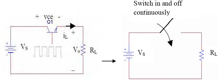
Switch in and off continuously 2.3 Switching converter
The disadvantages of using the linear regulator is it has low efficiency (<20%) when the input to output voltage differential are more converted into heat. To increase the efficiency, the switching converter can replace the linear regulator because it has higher efficiency which about 90%. Switching converter consists the transistor that acts as a switch (can be turned on and off) instead of as a variable resistance. The transistor in switching converter operates in cut-off and saturation region.
Figure 2.1 shows the actual switching converter and its equivalent circuits. The transistor acts as a switch that turns on and off continuously when it operates in cut-off and saturation region. The period is determined by the pulse-width’s duty cycle that being applied at the base of the transistor.
Figure 2.1 (a) Actual switching converter circuit (b) Switching converter equivalent circuit.
By assuming the switch is ideal, the output voltage is the same as the input voltage when the switch is on and zero when the switch is off. The DC component of the output voltage is calculated by using equations provided.
(2.1)
5
(2.3)
From the equation above, it can be conclude that the output voltage is depending on the duty ratio (D). The value duty ratio can be calculated as in equation (2.4) where f is the switching frequency, is the time when the switch is on, and T is time for one complete
cycle.
(2.4)
2.4 Buck converter
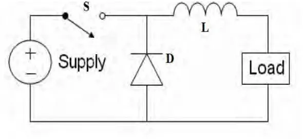
Buck regulator is a DC-DC converter that converts higher DC voltage to lower DC voltage or step-down DC-DC converter. It is also known as down converter because the output voltage is less than the input voltage. The converter consists of a diode (D), voltage supply, filter circuit of inductor (L) capacitor (C), and load (R). The fundamental buck converter circuit with an ideal switch (S) is being show in the Figure 2.2.
6
2.5 Buck basic circuit operation
The operation of an ideal buck regulator is to controlled the output voltage by becoming either completely alternate on or off. The operation of circuit when the switch is on (closed) is showed in Figure 2.3.
Figure 2.3: Buck converter when the switch is on (closed)
During switch is closed condition (short-circuited), the current flows from the source (input voltage) through the inductor to the load it return to the supply. The direction of the current when the switch is in condition is showed by an arrow in the Figure 2.3 above. In that condition, the diode will not conducts because it is in opened (reverse biased condition). Figure 2.4 shows the operation of circuit when the switch is off (opened).
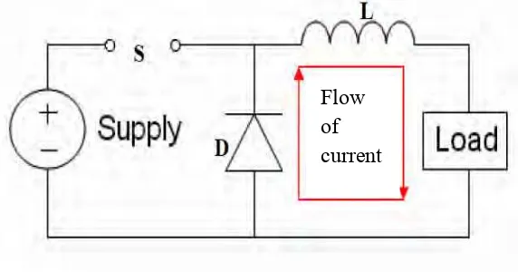
Figure 2.4: Buck converter when the switch is off (open) Flow
7
From Figure 2.4, when the switch is off (open-circuited), the energy stored in the inductor is released to the load and diode. Now the diode is in forward biased condition. The arrows in the figure shows the path of current that flow only through diode, inductor and to the load when the switch is off state. At a fixed value for output voltage regulation, the process will be repeated. Then the switch will operate in on state again before the current reaches zero for condition of continuous current mode (CCM) operations.
2.6 LED Driver Circuit
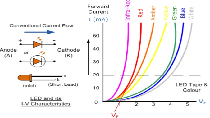
The brightness of Light Emitting diode (LED) will be control in terms of its output voltage stability to improve and maintain its efficiency. To run LED with desired output voltage, the LED driver circuit will be needed. An LED driver circuit is a self-contained power supply that has outputs matched to the electrical characteristics of LED or array of LED’s [2]. One of the disadvantages of LED is most of electrical energy supplied to the LED is converted to heat and this will increase its temperature. Hence, the circuit will become unstable when the LED resistance varies with the temperature. The unique characteristic of I-V curve for LED also becomes one of the weakness that need to be considered. Figure 2.5 shows the I-V curve for several colours of LEDs.
8
From Figure 2.5, it can be seen that the small changes of voltage output will cause a larger change of output current in LED. Hence, large change in current will reduce the stability of the LED when the current supplied to the LED exceeds its rating forward current. This will reduce the durability and efficiency of LED. In that case, it is important to maintain the output voltage in constant value in order to prevent large changes of LED current flow.
2.7 Orcad PSpice Software
Orcad PSpice is software that is used to create, produce and analyze both analog and digital electronic circuits. Many problems related to voltage and current can be solving effectively in the project by using this software. The designed from this software can be a good reference before transferred the circuit into hardware design. It also able to produce many type of waveform from the analyze circuit [3]. Figure 2.6 shows PSpice schematic window. The menu bar consists of menu like file, edit, view, tools, place and etc as shown in the figure.
Figure 2.6: Orcad PSpice schematic window
Place ‘last added’
part list Toolbar button or icons Menu Bar
9
Menu bar helps user to create a new design or schematic, search tools to add or modify the circuit design, saving the project and finally to simulate and analyze the project through waveform. Next, added part list is a box that keeps the last used of component throughout the entire file of design process that user have created. Then, the toolbar buttons function is to show the icons of the options in the menu bar and act as a shortcut to the menu bar options. Finally, the scroll allow user to scroll the window to view the hidden part in the schematic circuit.
2.8 Pulse Width Modulation (PWM)
The purpose of Pulse Width Modulation (PWM) technique is to control the switching rate and pulse width in buck converter circuit. PWM circuit consists of an oscillator and gated latch that has function to produce triangular waves and the signal then will be modulated to produce series of pulse signal to the switching element that will finally be fed to the Power MOSFET. Basic PWM circuit and the generation series of pulse from the triangular wave and control signal is shown in Figure 2.7 (a) and (b).