SIMULATION DEVELOPMENT OF A STEP DOWN DC CONVERTER BASED ON MULTICELL TOPOLOGY USING
PSIM9
Ahmad Ridhan Bin Ramli
SIMULATION DEVELOPEMENT OF STEP DOWN DC CONVERTER BASED ON MULTICELL TOPOLOGY USING PSIM 9
AHMAD RIDHAN BIN RAMLI
A report submitted in partial fulfillment of the requirements for the degree of Power Electronic and Drives
Faculty of Electrical Engineering
UNIVERSITI TEKNIKAL MALAYSIA MELAKA
ii
“I hereby declare that I have read through this report entitle “Simulation Development of Step Down DC Converter Based On Multicell Topology Using PSIM 9 (For Green Energy)” and
found that it has comply the partial fulfillment for awarding the degree of Bachelor of Electrical Engineering (Power Electronic and Drives)”
iii
I declare that this report entitle “Simulation Development of Step Down DC Converter Based On Multicell Topology Using PSIM 9 (For Green Energy)” is the result of my own research except as cited in the references. The report has not been accepted for any degree and is not
concurrently submitted in candidature of any other degree.
iv
DEDICATION
Special dedication goes to my beloved mother Puan Shamsuria Bte Ibrahim and my beloved father En. Ramli Bin Mohamad
For growing me up without, taking care of mend educating me all these while. Also thank for their continuous pray until I become what i’m now.
Also for my Family...
En. Mohd Khairi Bin Mohd Zambri Pn. Nurul Ain Bte Mohd Said
Thank you very much...
And not forgetting to all my relatives...
All of my friends especially Electrical Engineering batch 2009-2012
v
ACKNOWLEDGEMENT
First and foremost, I would like to express my hearty gratitude to my supervisor, Mr. Mohd Khairi Bin Mohd Zambri for the guidance and enthusiasm given throughout the progress of this project. Also guiding this project with clarity and that priceless gift of getting things done by sharing his valuable ideas as well as his knowledge.
I also would like to thank to all Universiti Teknikal Malaysia Melaka (UTeM) lecturers, electrical technicians, and my best colleagues which have provide assistance at various occasions. My appreciation also goes to my family who has been so tolerant and supports me all these semester. Thanks for their encouragement, love and emotional supports that they had given to me.
vi
ABSTRACT
Nowadays power electronics plays a very important role in many sectors including in industrial, office and household applications. Implementation of power electronics, include the use of static converters in very broad functions such as power supply, control of electric machines and others. But in some applications are only available resources with a high voltage rating that required a converter to switch the appropriate rating to supply the load, but the problem is because the semiconductor components with suitable voltage capability are not available. On the other hand, the need to increase the voltage level of electrical energy conversion system and the difficulties to increasing the voltage capability of semiconductor components, triggering the efforts to create new structures of static converters, one of the new structure is multicell converters. This new structure not allows conversion of high voltage electrical energy especially all problem related to the harmonics ripple.
vii
ABSTRAK
Pada masa kini elektronik kuasa memainkan peranan yang amat penting dalam banyak sektor termasuk dalam aplikasi industri, pejabat dan rumah. Pelaksanaan elektronik kuasa, termasuk penggunaan penukar statik dalam fungsi-fungsi yang sangat luas seperti bekalan kuasa, kawalan mesin elektrik dan lain-lain. Tetapi dalam sesetengah aplikasi hanya sumber-sumber yang sedia ada dengan kadar voltan yang tinggi yang memerlukan penukar untuk menukar penarafan yang sesuai untuk membekalkan beban, tetapi masalah ini adalah kerana komponen semikonduktor dengan keupayaan voltan yang sesuai tidak boleh didapati. Sebaliknya, perlu untuk meningkatkan tahap voltan sistem penukaran tenaga elektrik dan masalah untuk meningkatkan keupayaan voltan komponen semikonduktor, usaha untuk mewujudkan struktur baru penukar statik, salah satu struktur baru ini dikenali sebagai penukar multicell. Struktur baru ini tidak membenarkan penukaran tenaga elektrik voltan tinggi terutama semua masalah yang berkaitan dengan riak harmonik.
viii
TABLE OF CONTENTS
CHAPTER TITLE PAGE
ADMISSION ii
SUPERVISOR CONFIRMATION iii
ACKNOWLEDGEMENT iv
ABSTRACT v
ABTRAK vi
TABLE OF CONTENT vii
LIST OF FIGURES xii
LIST OF TABLES xvi
LIST OF SYMBOLS xvii
LIST OF APPENDICES xviii
1 INTRODUCTION 1
1.0 Introduction 1
1.1 Problem Statement 3
1.2 Objectives 3
1.3 Scope 4
2 LITERATURE REVIEW 5
2.1 Introduction of Power Electronic 5
2.2 Classification of Converter 6
2.3 Modulation Techniques 8
2.4 Harmonics 9
2.5 Buck Converter 11
2.6 Multilevel Converter Topology 13
2.6.1 Flying Capacitor Converter 14
ix
2.7.1 Introduction 16
2.7.2 Multicell Topology 17
2.7.3 IGBT 18
2.7.4 IGBT Structure 18
2.7.5 Total Harmonic Distortion 21
2.8 PSIM 9 Software 23
3 METHODOLOGY 24
3.1 Introduction 24
3.2 General Approach 24
3.3 Flow Chart 25
3.4 Project Design 26
3.5 Modulator of the Multicell Converter 27 3.5.1 The Switching Table of the Multicell Converter 28 3.6 Operation of DC-DC Multicell Converter 28
3.7 Filter Circuit 29
3.8 Mathematical Model of Multicell Converter 30
3.8.1 Two-Port Switching Network 30
3.9 Circuit Analysis 31
3.9.1 Two-Cell Case 31
3.10 Harmonic Analysis 33
3.11 Buck Converter Analysis 35
3.11.1 Circuit Description 35
3.11.2 Circuit Operation 36
3.11.3 Analytical Expression for Buck Converter 36 3.11.4 Advantage and Disadvantage of Buck Converter 38 3.12 Full-Bridge DC-DC Converter Analysis 39
3.12.1 Circuit Description 39
3.12.2 Circuit Operation 40
3.12.3 Analytical Expression for Full-Bridge Converter 41
x
3.14 Project Progress Flow Chart 44
3.15 Project Schedule 45
4 RESULTS 46
4.1 Introduction 46
4.2 Multicell Converter Topology Design 46
4.3 Simulation Results 47
4.4 Buck Converter Design 52
4.5 Modeling and Simulation of Buck Converter 53
4.6 Full-Bridge Converter Design 54
4.7 Modeling and Simulation of Full-Bridge Converter 55
5 ANALYSIS AND DISCUSSION 57
5.1 Introduction 57
5.2 Analysis on Output Dc Voltage of The Multicell Converter 57 5.3 Analysis Output Voltage of The Buck Converter 61 5.4 Analysis Output Voltage of The Full-Bridge Converter 66
5.5 Summary 69
5.6 Discussion 70
6 CONCLUSION AND RECOMENTDATION 72
6.1 Introduction 72
6.2 Conclusion 72
6.3 Recommendation 73
REFERENCES 74
APPENDIX A 76
xi
LIST OF FIGURES
FIGURE TITLE PAGE
2.2.1 A Source and Load Interfaced by a Power Electronics Converter 6 2.2.2 A Converter can Operate as Rectifier or an Inverter 7
2.3.1 Basic waveform for PWM 9
2.5.1 Buck Converter Circuit 11
2.5.2 Buck Converter DC Output voltage 13
2.6.1.1 Five Level Flying Capacitor Bridge Inverter 15
2.7.1. Multicell Converter Design 17
2.7.2.1 R-L-C series Circuit 18
2.7.4.1 Cross section 19
2.7.4.2 Equivalent circuit of IGBT 20
2.7.4.3 Simplified circuit of IGBT 20
2.7.4.4 Symbol and circuit for an IGBT 20
2.7.4.5 Collector-emitter voltage 21
2.7.5.1 Ideal Sine Wave 22
2.7.5.2 Distorted Waveform 22
3.3.1 Project Overview 25
3.5.1 Modulator of the Multicell Converter 27 3.6.1 The two- cell of Multicell Converter Design 29 3.7.1 LC filter circuit of Multicell Converter 29
3.8.1.1 Basic Two Port Switching Network 30
3.9.1.1 Two Cell Multicell Converter 31
3.9.1.2 Equivalent circuit in terms of d and t parameters 33
3.11.1 Buck Converter Design 36
3.12.1 Full-Bridge Converter Circuit 40
3.13.1 Project overview 44
xii
4.3.1.1 Output Waveform (DC voltage) 1 49
4.3.1.2 FFT Analysis from First Design 49
4.3.1.3 Output Waveform (DC voltage) 2 50
4.3.1.4 FFT Analysis from 2nd Design 50
4.3.1.5 Output Waveform (DC voltage) 3 51
4.3.1.6 FFT Analysis from 3rd Design 51
4.3.1.7 Output Waveform (DC voltage) for final stage 52
4.3.1.8 FFT Analysis from the final stage 52
4.5.1 Buck Converter Modeling 53
4.5.2 The output voltage of Buck Converter 54
4.5.3 FFT Analysis for Buck Converter 54
4.7.1 Full-Bridge Dc Converter Modeling 55
4.7.2 Output Waveform of Full-Bridge Converter 56 4.7.3 FFT Analysis for Full-Bridge Dc Converter 56
5.2.1 Output Voltage with peak time 0.812ms 59
5.2.2 Output Voltage with rise time from 0.2ms at 5V 60
5.2.3 Rise Time (Ts) of the output voltage 60
5.2.4 Output Voltage without Balance Booster 60 5.2.4 Comparison Output Voltage with Input Voltage 61
5.3.1 Buck Converter Modeling 63
5.3.2a Output Voltage of Buck Converter 63 5.3.2b Output Voltage of Multicell Converter 63 5.3.3a FFT Analysis of Multicell Converter 64 5.3.3b FFT Analysis of Buck Converter 64 5.3.4a The Peak Time output voltage of the Buck Converter with 0.74ms 64 5.3.4b The Peak Time output voltage of the Multicell Converter with
0.812ms 65
xiii
xiv
LIST OF TABLE
TABLE TITLE PAGE
2.6.1.1 Five Level Flying Capacitor Bridge Inverter Switching State 15
3.5.1.1 The switching State of Multicell Converter 28
3.15 Project Schedule 45
5.2.1 Parameters of Multicell Converter 59
xv
LIST OF SYMBOLS
C - Capacitor
DT - Duty Ratio
F - Farad
H - Henry
I - Current
L - Inductor
Μ - Micro
Ms - Millisecond
P - Commutation Cell
R - Resistor
THD - Total Harmonic Distortion
V - Volt
xvi
LIST OF APPENDIX
APPENDIX TITLE PAGE
A Calculation of the parameters of the converters 76
CHAPTER 1
INTRODUCTION
1.0 MULTICELL CONVERTER HISTORY
Multicell converters were introduced ten years ago and over this period, their properties have been thoroughly analyzed. This project summarizes the main results obtained through the research done on these converters over these periods: topology and derivation of multicell choppers and voltage source inverter, harmonics cancellation, open loop modulation techniques, self-balancing understanding and optimization. Since then, this concept have lead to some other innovative topologies which will be briefly presented in this project. Multilevel converter has been developed as a result of the increasing need for higher power converters. To achieve the power rating is higher, voltage and current capability of devices used in the converter must be increased. Current technology insulated gate bipolar transistor (IGBT) wide up to 6.5 kV, 900 per switching devices [1].
Multicell topology is formed when a number, the P cells change imprecated (overlapping) to form a leg inverter or chopper turn on input voltage of the converter circuit when the voltage is the same transformation of cells Vt / t. A general circuit topology shown in Figure 2.7.1 multicell. Depending on the trend to be an exception, the number of cells can be extended to cells of p. Output voltage waveform can be optimized with interference signals to control a variety of cells [1]. Output voltage waveform of the range of measures Vt / t and the frequency of single cell switching frequency, which reduces the output filter inductance
around . An important aspect to remember about that multicell topology is the balance booster. Introduce some booster circuit, basically called the notch filters are connected in parallel with the load. This notch filter's purpose is to provide the low impedance at multiples
2
2
of the frequency change. The most common form of the balance booster the series RLC circuit. The reason for the name of the balance booster, follows from the effect that this circuit have the balance voltage cell capacitor. If the circuit is designed to have low impedance at the frequency change, it means that the load impedance is smaller then the switching frequency as the parallel combination of load impedance and the impedance of the balance booster circuit. The theory developed in this paper provide a way to measure the effects of some booster [1].
Converters use a series of switches, allowing the use of switches to reduce the voltage. This low-voltage switches with low loss and shift to higher frequencies In many cases, active switching element has been used for harmonics current filtering. They operate using pulse width modulation (PWM) techniques to inject the required non-sinusoidal current requirements of nonlinear loads. Many studies have been carried out on various aspects of active power filter implementations. Parallel active power filters (PAF) normally operate using pulse width modulation (PWM) inverter techniques to inject the required non-sinusoidal current requirements of nonlinear load but are complex with the number of switches in use.
3
1.1 PROBLEM STATEMENT
1. The component is difficult to find and some of the component are not suitable voltage. 2. Other step-down converters are obtained lower band-width of switching frequency. 3. Other step-down converters could not improve the output of converter and it also could
not allow conversion of high voltage frequency electrical energy on the output side. 4. Other step-down converters also can play the same role as multicell topology such as a
single DC Chopper, but this topology is going to be a very high risk topology because if semiconductors are damaged in the converter, it could produce a high voltage from source directly to the load.
5. Other method does not obtain higher band-width of switching frequency. It also cannot reduce Total Harmonic Distortion (THD).
1.2 OBJECTIVE
The main objectives of this project are:
1. To use a low cost devices to replace old topology like Buck converter and Full-Bridge converter.
2. To obtain higher bandwidth of switching.
3. To make specific purpose of the DC-DC converter such as power supply for transportation.
4. To increase performance of the converter by inserting more switches.
4
1.3 SCOPE
CHAPTER 2
LITEATURE REVIEW
2.1 INTRODUCTION OF POWER ELECTRONICS
Power electronics convert electrical energy from one form to another electronic device. Function of power electronic circuits using semiconductor devices such as switches, control or modify the voltage or current. Power electronic applications of high power conversion equipment such as DC power supply to each of the hardware that is available at this time, such as cordless screwdriver, charger power supply for computers, mobile phones and hybrid cars. Power Electronics, including applications in which the circuit milliwatts or megawatts. Typical applications of power electronics, including AC to DC conversion, DC to AC conversion, the conversion voltage control voltage is controlled, and change the AC power source to the intensity and frequency to another frequency and the amplitude.
The design of power conversion equipment, including many of the disciplines of electrical engineering. Power electronic applications including circuit theory, control theory, electronics, microprocessor control and heat transfer. Semiconductor switching power expansion in combination with the required to improve efficiency and performance of electronic devices has made an important area of power electronics and expanded rapidly in the field of electrical engineering [1].\
2.2 CONVERTER CLASSIFICATION
6
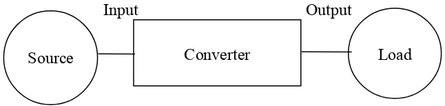
[image:23.595.136.459.71.148.2]Input Output
Figure 2.2.1 A Source and Load Interfaced by A Power Electronics Converter
Converters are classified by the relationship between the input and output:
2 AC input/DC output
The converter that converts an AC (input) to DC (output) is called converter. The power flows from AC sources and transferred it to a DC load. This converter is classified as rectifier. For the example, the converter integrated circuits to operate 50Hz AC line voltage by converting the AC signal to a DC signal.
3 DC input/AC output
The converter that converts a DC (input) to AC (output) is called inverter. The power flows from the DC source and transferred it to an AC load. The example of inverter applications is an array of solar cells. It produces a 120V from a 12V battery.
4 DC input/DC output
The DC (input) and DC (output) converter usually use as regulated. This converter is very useful when a DC load requires a specified voltage, but DC source have unregulated value. For the example, 12V load may be obtained to 24V source via DC-DC converter.
5 AC input/AC output
The converter that uses to charge level or frequency of AC signals is called as AC (input) - AC (output) converter. For the example, the speed control of ceiling fan and an induction motor.
Some of the converter circuit can operate in different ways, depending on the
7
circuit and control parameters. For example, modify the semiconductor devices, some recovery circuit can act as a converter. In Fig.2.2.2, the converter has the characteristics of the rectifier, if the battery is charged from an AC power source. Thus, in others, the converter is characterized as a converter, if the battery is a source of AC power supply for system [2].
Figure 2.2.2 A Converter can Operate as Rectifier or an Inverter
Power conversion can be a multifactorial process that involves more than one type of converter. For example, an AC-DC-AC conversion can be used to modify an AC power source by first converting to DC and then converting the signal into a DC signal that is AC frequency range and different from those original source of AC power.