Effect of a Discrete PIN Diode on Defected Ground
Structure
M.H Abdul Hadi
1, B. H. Ahmad
1, N. A. Shairi
1,Peng Wen Wong
2Centre for Telecommunication Research &Innovation1 Faculty of Electronics and Computer Engineering
UniversitiTeknikal Malaysia Melaka (UTeM) Hang Tuah Jaya, 76100 Durian Tunggal, Melaka, Malaysia.
[email protected], [email protected], [email protected]
Electrical & Electronic engineering Department2 UniversitiTeknologi PETRONAS (UTP) Bandar Seri Iskandar, 31750 Tronoh, Perak, Malaysia.
Abstract—This paper investigates the effect of a discrete PIN diode on Defected Ground Structure (DGS) where the different resonant frequency between ON and OFF state of the PIN diode is observed. Analytical modeling is determined and analyzed based on equivalent circuit of PIN diode and DGS. Then, a circuit simulation is performed using simulation software with different value of inductance and capacitance of DGS during ON and OFF state of the PIN diode. As a result, the resonant frequency of the PIN diode on the DGS shifted to higher frequency during ON state and shifted to lower frequency during OFF state. Besides, a larger value of inductance with a smaller value of capacitance of DGS will produce a larger range of resonant frequency between ON and OFF state and vice versa.
Keywords—defected ground structure; DGS; PIN diode; resonant frequency; RF switch
I. INTRODUCTION
Over the years, Defected Ground Structure (DGS) provides a significant advantage by extending its applicability such in amplifiers [1, 2], filters [3, 4], power dividers [5], couplers [6, 7], and switches [8-10]. DGS is implemented by modifying guided wave characteristics where it changes the propagation constant and realized by etching only a few areas on the ground plane under a microstrip line [11]. The previous research works in [12, 13] reported the effects of lumped element on DGS. The selected lumped elements are chip type resistor, inductor and capacitor. However, there are other active components such as PIN diode, varactor diode or transistor which can be investigated its effects on DGS.
Therefore, this paper investigates the effect of discrete PIN diode on DGS. Fig. 1 shows a discrete PIN diode where it is placed on the dumbbell shaped DGS. Theoretically, the inductance and capacitance of DGS should create resonant response with the PIN diode during ON and OFF state. Two squares of etched area represent inductance while a gap between two squares represents capacitance [11].The investigation is the resonant frequency of discrete PIN diode on DGS based on analytical modeling and circuit simulation.
Fig. 1. Example of a discrete PIN diode on dumbbell shaped DGS.
II. ANALYTICAL MODELING
Fig. 2 shows the equivalent circuits of discrete PIN diode during ON and OFF state [14] on equivalent circuit of DGS [15, 16]. The total impedance of the equivalent circuit is derived. Then scattering parameter (S-parameter) between Port 2 and Port 1 (S21) is explained using transmission (ABCD) matrix and conversion between ABCD to S-parameter in order to study the effect of discrete PIN diode on DGS.
(a)
(b)
Fig. 2. Equivalent circuit of discrete PIN diode on DGS during (a) ON state and, (b) OFF state.
From Fig. 2(a) and 2(b), Ls and Rf denotes as a series inductance and forward resistance respectively during ON state while Rr is a reverse resistance and Cj is junction capacitance during OFF state of the discrete PIN diode. In DGS equivalent circuit, LDGS and CDGS refer to inductance and capacitance of DGS. Note that Cp value is very small, so it is neglected in analytical modeling. During ON or OFF state, the general total impedance of the equivalent circuit is
(1)
From (1), the total impedance of the equivalent circuit during ON state is
(2)
From (2), using ABCD matrix and conversion between ABCD to S-parameter the S21 is derived as
(3)
The same steps are used on the equivalent circuit during OFF state where
(4)
Then, from (4), the S21 is derived as
(5)
During OFF or ON state, by refering to (1), a resonant frequency of discrete PIN diode on DGS occurs when
0 (6)
From (6), the resonant frequency can be calculated as
(7)
From (3) and (5), it is found that the resonant frequency during ON and OFF state will be different to each other due to the presence of Cjduring OFF state of PIN diode. Thus, the resonant frequency during OFF state is theoretically will be shifted to lower frequency due to larger value of CT compared with resonant frequency during ON state.
III. CIRCUIT SIMULATION
The circuit simulation is performed in Advanced Design System (ADS) software based on the equivalent circuit in Fig. 2(a) and 2(b). In the simulation, PIN diode model is based on commercialized PIN diode from NXP Semiconductors (part number: BAP64-02). The +5 V and -5 V of voltage supplies are used to turn ON and turned OFF the PIN diode respectively. The PIN diode model in ADS software has parameters of Cj = 0.35 pF, Ls = 0.6 nH, Rr = 5 Ω and Rf = 1 Ω.
For the equivalent circuit of DGS, it is well known that the effective inductance of the dumbbell shaped DGS pattern increases with larger square areas (a and b), while its effective capacitance increases with a narrower gap width in the middle (g) [17]. The DGS design is obtained through parametric study as reported in [18-19] since there is no specific synthesis to obtain the layout size of DGS. This technique is also very popular in antenna designs [20-22].
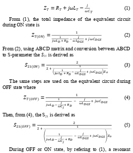
Therefore, inductance and capacitance of DGS are varied to be resonated at 4.0 GHz where five values of inductance are chosen; 10 nH, 8 nH, 6 nH, 4 nH and 2 nH. Then, the capacitance of DGS is tuned at 4.0 GHz. Fig. 3 shows simulation results of DGS at resonant frequency of 4.0 GHz. Table 1 shows the different values of inductor and capacitor at 4.0 GHz for Fig. 3.
Fig. 3. Resonant frequency of DGS at 4.0 GHz.
TABLE I. INDUCTANCE AND CAPACITANCE OF DGS AT RESONANT
FREQUENCY OF 4.0GHZ
Values of Inductance and Capacitance of DGS
Inductance, L (nH) Capacitance, C (pF)
10.0 0.16 8.0 0.20 6.0 0.26 4.0 0.40 2.0 0.78
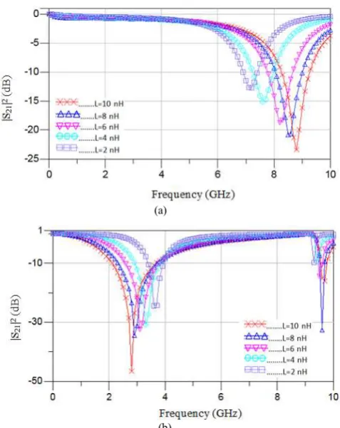
From Table I, values of L and C of DGS are used to investigate the resonant effect of PIN diode during ON and OFF state due to DGS. Thus, Fig. 4 shows the simulation results of discrete PIN diode on DGS during ON and OFF state.
(a)
(b)
Fig. 4. Simulation results of equivalent circuit during (a) ON state and, (b) OFF state.
(a)
(b)
(c)
Fig. 5. Range of resonant frequency between ON and OFF state at different value of L and C of DGS; (a) L = 10 nH, C = 0.16 pF (b) L = 6 nH, C = 0.26 pF and (c) L = 2 nH, C = 0.78 pF.
To further the investigation, a circuit simulation is carried out to compare the performance of PIN diode with and without DGS during ON and OFF state. A pair of inductance, L = 10 nH and capacitance, C = 0.16 nH (refer Table I) is chosen to incorporate with the PIN diode model. Fig. 6 shows simulation results of PIN diode with and without DGS during ON and OFF state.
(a)
(b)
Fig. 6. Simulation results ofPIN diode with and without DGS during (a) ON state, and (b) OFF state.
IV. DISCUSSION
ON state which explains the low insertion loss[23].Furthermore, during ON state, it removes the parasitic capacitance and leaves PIN diode in low impedance state [24].
During OFF state, by incorporating DGS to PIN diode, it enhances the isolation performance of PIN diode where the DGS resonates out parasitic capacitance of PIN diode. It is shown in Fig. 6(b) where the circuit simulation of PIN diode with DGS (during OFF state) effectively improve isolation performance compare with PIN diode itself. Inductance and capacitance of DGS are able to resonate at any desired frequency as shown in Fig. 3.Note that the second resonance can be seen in Fig. 4 and 5. This scenario is not due to the effect of DGS but the characteristic of commercialized PIN diode from NXP Semiconductor.
In Fig. 4(a), during ON state, the resonant frequency has shifted to higher frequencies due to parallel Ls and LDGS that produces smaller total inductance, LT (refer Fig. 2(a)). In Fig. 4(b), during OFF state, the resonant frequency has shifted to lower frequencies due to parallel Cj and CDGS that produces larger total capacitance, CT (refer Fig. 2(b)). Besides, it can be observed that both Fig. 4(a) and 4(b) have different resonant frequency locations due to different values of L and C of DGS. Furthermore, the different values of L and C of DGS have produced different range of resonant frequency between ON and OFF state. In Fig. 5(a), 5(b) and 5(c), the range of resonant frequency between ON and OFF state are 6.8 GHz, 5.1 GHz and 3.6 GHz respectively. Thus, larger value of inductance with smaller value of capacitance of DGS (e.g. L = 10 nH and C = 0.16 pF) produces a larger range of resonant frequency between ON and OFF state.
V. FUTURE WORK
The next step is to verify this investigation with EM simulation and S-parameter measurement. The PCB substrate material will be based on FR4 material which is low cost as reported in [25, 26].In term of application, we found that it has a potential to be applied in RF switch design. Since the DGS is also acts as a resonator, it will have a similar solution for isolation improvement of FET or PIN diode switches as reported in [27-30]. The FET or PIN diode switches can be applied in wireless communication [31, 32], microwave imaging [33, 34] and test system [35, 36].
VI. CONCLUSION
Analytical modeling and circuit simulation of discrete PIN diode on DGS have been presented in order to investigate the resonant frequency of the circuit. Different value of inductance and capacitance of DGS are determined for different resonant frequency during ON and OFF state of PIN diode. Therefore, we conclude that resonant frequency of the PIN diode on DGS has shifted to higher frequency during ON state and shifted to lower frequency during OFF state. Besides, a larger value of inductance with a smaller value of capacitance of DGS produces a larger range of resonant frequency between ON and OFF state and vice versa.
ACKNOWLEDGMENT
We would like to acknowledge the contribution of our colleagues from Faculty of Electronics and Computer
Engineering, UTeM of the research work. This work is funded by Fundamental Research Grant Scheme (FRGS), Ministry of Higher Education, Malaysia (project number FRGS/2012/FKEKK/TK02/03/2/F00128).
REFERENCES
[1] Sung Min Kang; Jae Hong Choi; Kyung Heon Koo; Sang Wook Nam, "A novel 5GHz and 2.4GHz dual band transmitter using microstrip defected ground structure," Microwave Symposium Digest, 2005 IEEE MTT-S International, 12-17 June 2005.
[2] Jong-Sik Lim; Ho-Sup Kim; Jun-Seok Park; Dal Ahn; Sangwook Nam, "A power amplifier with efficiency improved using defected ground structure," Microwave and Wireless Components Letters, IEEE , vol.11, no.4, pp.170-172, April 2001.
[3] Zakaria, Z.; Shairi, N.A.; Sulaiman, R.; Sam, W.Y., "Design of reconfigurable defected ground structure (DGS) for UWB application,"
Applied Electromagnetics (APACE), 2012 IEEE Asia-Pacific Conference on , pp.195-198, 11-13 Dec. 2012.
[4] Banciu, M.G.; Militaru, N.; Lojewski, G., "Defected Ground Dual-Mode Resonators and Filters," Personal, Indoor and Mobile Radio Communications, 2007. PIMRC 2007. IEEE 18th International Symposium on, pp.1-5, 3-7 Sept. 2007.
[5] Jong-Sik Lim; Sung-Won Lee; Chul-Soo Kim; Jun-Seok Park; Dal Ahn; Sangwook Nam, "A 4.1 unequal Wilkinson power divider," Microwave and Wireless Components Letters, IEEE , vol.11, no.3, pp.124-126, March 2001.
[6] Militaru, N.; Banciu, M.G.; Du u, C. A.; Trupina, L.; Lojewski, G., "Compact Wireless Devices with Defected-Ground Structures," Wireless and Mobile Communications, 2006. ICWMC '06. International Conference on, pp.85-85, 29-31 July 2006.
[7] Jong-Sik Lim; Chul-Soo Kim; Jun-Seok Park; Dal Ahn; Sangwook Nam, "Design of 10 dB 90° branch line coupler using microstrip line with defected ground structure," Electronics Letters , vol.36, no.21, pp.1784-1785, 12 Oct 2000.
[8] Kang, Byeong-Gwon; Jun-Seok Park; Hoon An; Kim, Sun-Hyung; Dal Ahn, "Design of RF switch with defected ground structure," Microwave Conference, 2000 Asia-Pacific , pp.165-168, 2000.
[9] Dong-Wook Kim, “Small-Sized High Power PIN Diode Switch with Defected Ground Structure for Wireless Broadband Internet”, ETRI Journal, Volume 28, Number 1, February 2006.
[10] Shairi, N.A.; Ahmad, B. H.; Abdul Aziz, M.Z.A.; Osman, A. F., "SPDT switch with defected ground structure for time division duplex switching in wireless data communication system," RF and Microwave Conference (RFM), 2011 IEEE International , pp.238-241, 12-14 Dec. 2011. [11] Chul-Soo Kim; Jun-Seok Park; Dal Ahn; Lim, Jae-Bong, "A novel 1-D
periodic defected ground structure for planar circuits," Microwave and Guided Wave Letters, IEEE , vol.10, no.4, pp.131-133, Apr 2000. [12] Dal Ahn; Chul-Soo Kim; Kim, Guen-Young; Jun-Seok Park, "Effects of
a Lumped Element on Defected Ground Structures," Microwave Conference, 2000. 30th European , pp.1-4, Oct. 2000.
[13] Jonguk Kim; Jong-Sik Lim; Kwangsoo Kim; Dal Ahn, "Effects of a Lumped Element on DGS with Islands," Microwave Symposium Digest, 2006. IEEE MTT-S International , pp.1145-1148, 11-16 June 2006. [14] D. M. Pozar, Microwave Engineering. Hoboken, NJ: John Wiley &
Sons, 2005. page 515 -516.
[15] Jong-Im Park; Chul-Soo Kim; Juno Kim; Jun-Seok Park; Yongxi Qian; Dal Ahn; Itoh, T., "Modeling of a photonic bandgap and its application for the low-pass filter design," Microwave Conference, 1999 Asia Pacific , pp. 331-334 vol.2, Nov 1999.
[16] L. H. Weng, Y.-C. Guo, X.-W. Shi, and X.-Q. Chen, "An overview on defected ground structure," Progress In Electromagnetics Research B, Vol. 7, 173-189, 2008.
[18] Elboushi, A.; Haraz, O.M.; Sebak, A.; Denidni, T.; , "Triangular shaped power divider for C-band operation using Defected Ground Structure (DGS)," Antenna Technology and Applied Electromagnetics & the American Electromagnetics Conference (ANTEM-AMEREM), 2010 14th International Symposium on , pp.1-4, 5-8 July 2010.
[19] Hajilou, Y.; Hassani, H.R.; Rahmati, B., "Introducing a novel defected ground structure for microstrip applications," Antennas and Propagation (EuCAP), 2013 7th European Conference on , pp.3472-3475, 8-12 April 2013.
[20] Xue-jie Liao; Hong-Chun Yang; Na Han; , "An improved dual band-notched UWB antenna with a parasitic strip and a defected ground plane," Intelligent Signal Processing and Communication Systems (ISPACS), 2010 International Symposium on , pp.1-4, 6-8 Dec. 2010. [21] B. H. Ahmad, M. M. Ariffin, H. Nornikman, N. M. S. Roslan, M. Z. A .
Abd Aziz, M. A. Atiqa, A. R. Ayuni, Y. W. Ming, " Parametric Study on the Compact G-Shaped Monopole Antenna for 2.4 GHz and 5.2 GHz Application", International Journal of Engineering and Technology (IJET), Vol. 5, No. 1, page 512-518, 2013.
[22] Abd.Aziz, M.Z.A.; Shukor, M.Md.; Suaidi, M.K.; Ahmad, B.H.; Othman, M.A.; Hasan, N., "Design a 3.5 slot antenna using coplanar waveguide (CPW) for dual band application," Microwave Techniques (COMITE), 2013l Conference on , pp.31-35, 17-18 April 2013. [23] W. E. Doherty, Jr., R. D. Joos. The PIN Diode Circuit Designers’
Handbook. Microsemi Corporation. 1998.
[24] Kadowaki, Yoshinobu. "Microwave semiconductor device." U.S. Patent No. 5,057,805. 15 Oct. 1991.
[25] Rahman, T.A.; Ibrahim, I.M.; Pak Siau Wei; Ahmad, J.; Wahab, A.G.C., "A study on effectiveness of FR4 as a dielectric material for radial line slot array antenna for wireless backhaul application," Communications (APCC), 2011 17th Asia-Pacific Conference on , pp.385-388, 2-5 Oct. 2011.
[26] M.H. Misran, M.A. Meor Said, M.A. Othman, M.M. Ismail, H.A. Sulaiman, K.G. Cheng, "Design of Low Noise Amplifier using Feedback and Balanced Technique for WLAN Application," Procedia Engineering, Volume 53, Pages 323-331, 2013.
[27] Tsukahara, Y.; Amasuga, H.; Goto, S.; Oku, T.; Ishikawa, T.; , "60GHz High Isolation SPDT MMIC switches using shunt pHEMT resonator,"
Microwave Symposium Digest, 2008 IEEE MTT-S International , pp.1541-1544, 15-20 June 2008.
[28] Shairi, N.A.; Ahmad, B.H.; Zakaria, Z.; Peng Wen Wong, "Isolation improvement of SPDT discrete switch with single switchable open stub resonator at 2 GHz band," Wireless Technology and Applications (ISWTA), 2012 IEEE Symposium on , pp.51-55, 23-26 Sept. 2012. [29] Shairi, N.A.; Ahmad, B.H.; Peng Wen Wong; , " Switchable Radial Stub
Resonator for Isolation Improvement of SPDT Switch", International Journal of Engineering and Technology (IJET), Vol. 5, No. 1, page 460 - 467, 2013.
[30] Shairi, N.A.; Ahmad, B.H.; Zahari, M.K.; Peng Wen Wong, "The potential application of switchable matched parallel-coupled stub resonator in SPDT discrete switch design," Applied Electromagnetics (APACE), 2012 IEEE Asia-Pacific Conference on , pp.372-376, 11-13 Dec. 2012.
[31] Ke Zhou; Jianyi Zhou; Zhiming Xu; , "Design of a high performance RF transceiver for TDD-LTE system," Microwave Symposium Digest (MTT), 2012 IEEE MTT-S International , pp.1-3, 17-22 June 2012. [32] Isa, A.A.M.; Markarian, G.; Isa, M.S.M.; Zakaria, Z.; Zin, M.S.I.M.,
"Simulation of virtual MIMO base stations for mobile location in IMT-Advanced networks," Applied Electromagnetics (APACE), 2012 IEEE Asia-Pacific Conference on , pp.176-181, 11-13 Dec. 2012.
[33] Kharkovsky, S.; Kam, K.; Ghasr, M.T.; McClanahan, A.D.; Abou-Khousa, M.A.; Zoughi, R.; Perez, I., "Microwave resonant switched-slot probe with perpendicular coaxial feed," Instrumentation and Measurement Technology Conference (I2MTC), 2010 IEEE , pp. 1299-1303, 3-6 May 2010.
[34] Abou-Khousa, M.A.; Ghasr, M.T.; Kharkovsky, S.; Pommerenke, D.; Zoughi, R., "Modulated Elliptical Slot Antenna for Electric Field Mapping and Microwave Imaging," Antennas and Propagation, IEEE Transactions on , vol.59, no.3, pp.733-741, March 2011.
[35] Lim Chee Chiang; Shairi, N.A., "The development and challenges of millimeter wave test system for package level," Applied Electromagnetics, 2007. APACE 2007. Asia-Pacific Conference on , pp. 1-5, 4-6 Dec. 2007.