i PARAMETRIC EFFECT OF DEFECTED GROUND STRUCTURE (DGS) ON
6GHZ OF A BANDPASS FILTER
NOOR AMRINA BINTI MOHD IJTIHAD
Fakulti Kejuruteraan Elektronik dan Kejuruteraan Komputer Universiti Teknikal Malaysia Melaka
ii
PARAMETRIC EFFECT OF DEFECTED GROUND STRUCTURE (DGS) ON 6GHZ OF A BANDPASS FILTER
NOOR AMRINA BINTI MOHD IJTIHAD
This Report Is Submitted In Partial Fulfillment of Requirement for the Bachelor Degree of Electronic Engineering (Wireless Communication) With
Honours
Fakulti Kejuruteraan Elektronik Dan Kejuruteraan Komputer Universiti Teknikal Malaysia Melaka
vi
To my beloved parents and family, Supervisor, all FKEKK lecturers and my friends for their continuous support, advice, and guidance to complete
vii
ACKNOWLEDGEMENT
In the Name of Allah, most Gracious, most Merciful.
Alhamdulillah, all of honors are just for Allah Azza Wajalla, the almighty, because gives His blessing for me within strength and enough time in finishing this final year report with titled “Parametric Effect of Defected Ground Structure (DGS) on 6GHz of a Bandpass Filter”.
viii
ABSTRACT
ix
ABSTRAK
x
TABLE OF CONTENT
CHAPTER TITLE
PAGE
TITLE OF PROJECT ii
DECLARATION iv
DEDICATION vi
ACKNOWLEDGEMENT vii
ABSTRACT viii
ABSTRAK ix
TABLE OF CONTENT x
LIST OF TABLES
xiii
LIST OF FIGURES
xiv
LIST OF ABBREVIATIONS xvii
I. INTRODUCTION
1.1 Project Background 1
1.2 Objective of the Project 2
1.3 Problem Statement 2
xi
1.5 Structure of the project 3
II. LITERATURE REVIEW
2.1 Introduction 5
2.2 C-Band 6
2.3 RF and microwave filter 8
2.3.1 Lowpass Filter 8
2.3.2 Highpass Filter 8
2.3.3 Bandpass Filter 8
2.3.4 BandstopFfilter 8
2.4 Design Method Prototype 10
2.5 Bandpass Transformation 11
2.6 Filter Implementation 12
2.7 Microstrip Transmission Line 12
2.8 Defected Ground Structure 13 2.9 Advance Design System Software 15
III. METHODOLOGY
3.1 Introduction 16
3.2 Flowchart 17
3.3 Design Process 20
3.4 Step to Design Filter by Using Advance Design
System (ADS) 21
3.5 Design of the Bandpass Filter 30
xii 3.5.2 Design Specification 30
IV. RESULT AND ANALYSIS
4.1 Introduction 31
4.2 Design Parameter 31
4.3 Design Calculation 30
4.3.1 Transformation to Bandpass Filter 34 4.3.2 Filter Realization with Microstrip
Technology 36
4.4 Schematic Layout 39
4.5 Simulation Result 40
4.4 Design the DGS 42
4.5 The Final Result of Bandpass Filter Open Loop
Dumbbell Shaped DGS 50
4.6 Fabrication and Measurement 51
V. FUTURE WORK AND CONCLUSION
5.1 Introduction 57
5.2 Conclusion 57
5.3 Future Work 58
xiii
LIST OF TABLES
NO TITLE
PAGE
Table 3.1: Parameters substrate of FR4 30
Table 3.2: Design Specification of Bandpass Filter 30
Table 4.1: C Element values for N = 5 33
Table 4.2: Calculated value of lumped component in parallel and serial 35 Table 4.3: Calculated value of J , Z oe , and Z oo 37 Table 4.4: Calculated dimension of transmission line 38
xiv
LIST OF FIGURES
NO TITLE
PAGE
2.1 Frequency band 7
2.2 Applications of satellite comunication 7
2.3 Type of microwave filter 9
2.4 Bandpass filter 9
2.5 Transformation of lumped element from lowpass prototype
into bandpass prototype 11
2.6 Dimension of microstrip transmission line (front view) 12 2.7 Dimension of microstrip transmission line (side view) 13 2.8 Innovation of Agilent Technologies within a period of year 15
3.1 Flowchart of the project 18
3.2 Workspace directory 21
3.3 Create workspace name 22
3.4 Select the libraries to include in the workspace 22 3.5 Choose a name for the workspace’s library 23 3.6 Select ‘Finish’ after done all the setup 24
3.7 File view of the workspace 24
3.8 Create a new schematic cell 25
xv 3.10 Import the component from the component library 26 3.11 Insert the component and connect them with wire 27
3.12 Circuit design 27
3.13 Transmission line calculator (LineCalc) 28 3.14 Choose the type of pallete to get the result simulation
3.15 Graph of result simulation 35 4.1 Attenuation Vs normalized frequency for chebyshev
filter response 33
4.2 Element values for 0.5dB equal ripple 34
4.3 0.5 dB equal ripple lowpass prototype 34
4.4 Schematic diagram of BPF using L & C values of network 39
4.5 Parallel coupled bandpass filter model 39
4.6 The parallel coupled bandpass filter layout 40 4.7 Simulated result of the lumped element of the bandpass filter 41 4.8 The simulated result of conventional parallel coupled of
the bandpass 42
4.9 the defected ground structure (DGS) layout by using
ADS 2011 43
4.10 The defected ground structure (DGS) with the
parameter L, W, and g 43
4.11 Single design of open loop dumbbell shaped DGS 44 4.12 Double design of open loop dumbbell shaped DGS 44 4.13 Simulation result for return loss with W= 1.3mm 45 4.14 Simulation result for insertion loss with W= 1.3mm, 45
xvi 4.17 Simulation result for return loss with W= 1.3mm 47
4.18 Simulation result for insertion loss with W= 1.3mm 47
4.19 Simulation result for return loss with W= 1mm 48 4.20 Simulation result for insertion loss with W= 1mm 48 4.21 Result simulation for parallel coupled bandpass filter with
single design of open loop dumbell shaped DGS 50 4.22 Result simulation for parallel coupled bandpass filter
with double design of open loop dumbell shaped DGS 51 4.23 Fabricated parallel coupled bandpass filter with single
design of open loop dumbell shaped DGS (a) front
(b) back 51
4.24 Fabricated parallel coupled bandpass filter with double
design of open loop dumbell shaped DGS (a) front (b) back 52
4.25 Vector Network analyzer 53
4.26 Measurement result of conventional parallel coupled
bandpass filter 54
4.27 Measurement result for parallel coupled bandpass filter
with single design of DGS 55
4.28 Measurement result for parallel coupled bandpass filter
xvii LIST OF ABBREVIATIONS
ADS - Advanced Design System DGS - Defected Ground Structure EBG - Electronic Band Gap EM - Electromagnetic FR4 - Fire Retardant 4 QoS - Quality of Service
1
CHAPTER I
INTRODUCTION
1.1 Project background
Nowadays, the modern of telecommunication technology developed more frequently rise and increases the biggest market demand. The governmental effort supportly toward the invention and innovation of new application in wireless communication. The examples of wireless communication include in microwave application, satellite application and WiMAX. These new application offer the good advantage and improvement in the telecommunication services and it offer the three important items to the customer which are coverage, capacity and Quality of Service (QoS). In term of coverage, the customer get the minimal signal level of electromagnetic waves. For the capacity, the rate of uploading and downloading more satisfactory and adequate to the customer. Then, the good quality of service (QoS) provide with no error of transmission of data as well so that no problem occurred to the service. [5]
2 Electromagnetic Band gap (EBG). DGS mostly used in many microwave design technique due to simple in it modelling rather than EBG.
In this project, the microstrip Bandpass Filter with Open Loop Dumbbell shaped Defected Ground Structure (DGS) for 6GHz was designed. The DGS was put in the metallic ground plane of planar transmission line. This DGS will disturb the shield current distribution in the ground plane cause of the defect in the ground. [8]Then, this disturbance will modify characteristic of transmission line and it will ensure the effective capacitance and inductance were produced.
1.2 Objective of the Project
This project embarks on the objectives that are listed below:-
i- To study and understanding of Bandpass filter and Defected Ground Structure (DGS).
ii- To design, fabricated and analyze the Bandpass filter with Open Loop Dumbbell Shaped Defected Ground Structure (DGS).
iii- To investigate the parametric effect of Open Loop Dumbbell Shaped Defected Ground Structure (DGS) on 6GHz of a Bandpass filter. iv- To gain the knowledge and experience on how to use ADS 2011 to
simulate the Bandpass filter.
1.3 Problem Statement
3 must provide the service with less number of interference among the users to achieve the high quality of service (QoS).
Emerging application in this system continue to challenge RF/ Microwave filter with ever requirement higher performance, smaller size, lighter weight and lowest cost. The desired specification of the microwave filter have to achieve in order to provide the smoothly and faster of transmitting information of signal to the customer around the world.
1.4 Scope of Project
This project will focus on several scope of work: i- Hardware part
- using FR4 board as substrate with permittivity of 4.4, thickness of 1.6mm and copper thickness of 0.035mm.
ii- Software part
-using Advanced Design System (ADS) 2011
1.5 Structure of the project
This report will divided into five main chapter. The first chapter discussed about the introduction of the project. Introduction includes the project background, problem statement, objectives of the project, and scope of project. Introduction act as the initial overview of the overall project.
The second chapter discussed about the literature review. In this chapter, the previous journal and article related to Bandpass filter and defected ground structure will be elaborated more detail to gain the specified information to this project.
4 process very important in order to make sure the project is conducted can achieved the goal and objective of the project.
Then, the forth chapter will discuss on result and discussion of the project. The result from the simulation of software and hardware will put in this chapter. The output expected value and measured value will be compared between both element of software and hardware.
5
CHAPTER II
LITERATURE REVIEW
2.1 Introduction
6
2.2 C-Band
The C band is often used to provide fixed communications and broadcast services. This band also provides a number of important strategic services including maritime communications, aeronautical services along with robust and reliable Virtual Private Networks (VPNs) for government and private corporations. It also provides vital connectivity services such as backhaul and rural telephony to remote areas. C band is the focus of next-generation satellite services in many rural areas. Rugged IP networks for banks and other businesses are being developed using C band spectrum.
Many regions rely heavily on the use of C band satellite capacity. Other frequencies such as Ku band (11/14 GHz) are readily available in other parts of the world and some regions rely heavily on it for backhaul services. However, the lack of Ku-band satellite coverage and terrestrial fiber in some regions means that there is no other option than the C band for offering many essential services. Users of receive-only satellite antennas have no need for license and are not registered with the regulator. This means that the total usage of C band satellite services is impossible to measure.
7
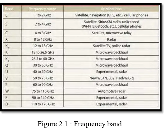
C-band is a band that allocated frequencies from 4GHz up to 8GHz. Primarily, C-band is used for full time TV satellite network. Commonly this band use in the tropical rainfall because it have the characteristic less dispose to rain fade rather than Ku band. [4]
Figure 2.1 : Frequency band