AS A REAL TIME OPTICAL SENSOR
FOR SUGAR SOLUTION CONCENTRATION DETECTION
MAMAT RAHMAT
GRADUATE SCHOOL
I hereby declare that the thesis of “Design and fabrication of one-dimensional photonic crystal as a real time optical sensor for sugar solution concentration detection” is my work with the direction of the supervising committee and has not
been submitted in any form to any college. Sources of information derived or quoted from the work published or not published by other authors mentioned in the text and listed in the refference at the end of this thesis.
Bogor, Desember 2009
Mamat Rahmat
MAMAT RAHMAT. Design and fabrication of one-dimensional photonic crystal as a real time optical sensor for sugar solution concentration detection. Supervised by HUSIN ALATAS, dan IRMANSYAH
A previous theoretical study of a finite one-dimensional photonic crystal composed of 12 unit cells with two defects had shown the existence of Photonic Pass Band (PPB) inside the Stop Band, which was suggested as a useful refractive index sensor due to the sensitive variation of PPB with respect to the change of refractive index of either defect layer material. We report in this presentation our successful fabrication of a prototype of this system by means of electron beam evaporation equipment in a sample chamber at pressure of 10-3 Pa with BK-7 glass substrate at temperature 573 K. Each of the photonic cells is composed of a high index layer of OS-5 with refractive index of n2.10, and an equal optical
thickness low index layer of MgF2 with n1.38. In the first defect cell, the high
index layer has twice the thickness of the other layers with the low index layer left unchanged, while in the second defect cell separated by 6 unit cells, the first layer is void to be filled with the sample solution. The device was used for measuring the refractive index of sugar solution with concentration range of 20-100 g/L in the real time mode. The result was found to achieve determination coefficient up to 98%. Further measurement performed has demonstrated a result in good agreement with theoretical prediction reported previously.
MAMAT RAHMAT. Design and fabrication of one-dimensional photonic crystal as a real time optical sensor for sugar solution concentration detection. Supervised by HUSIN ALATAS, dan IRMANSYAH
This study is developed from the results of theoretical study of one-dimensional photonic crystals with two defects that have unique characteristics in response of Photonic Band Pass (PPB) on the frequency interval of Photonic Band Gap (PBG). This study focused on prototyping photonic crystal sensor based on refractive index changes in a second defect that serves as a receptor in which to respond transmitansi value changes, so that could be used as a single-frequency index sensing. The reference wavelength that used in this study is 525 nm.
This research was conducted with some of the following stages: theoretical model of observation through implementation and simulation, fabrication of photonic crystal, characterization, sensing test, assembly and instrumentation devices, and device performance measurement. Fabrication process of a prototype of this system by means of electron beam evaporation equipment in a sample chamber at pressure of 10-3 Pa with BK-7 glass substrate at temperature 573 K. Each of the photonic cells is composed of a high index layer of OS-5 with refractive index of n2.10, and an equal optical thickness low index layer of
MgF2 with n1.38. In the first defect cell, the high index layer has twice the
thickness of the other layers with the low index layer left unchanged, while in the second defect cell separated by 6 unit cells, the first layer is void to be filled with the sample solution.
This research shown that the prototype of one-dimension photonic crystal with two defects could be implemented as an optical sensor to measure a certain solution's concentration. In this case, we used sugar solution with the concentration range from 20 to 500 g / L and the measured refractive index between 1.332 and 1.415 as a sample target. To analyze the result, we used the linear regression method. We divide the data into a linear two areas: the first is the area with 20-100 g / L and, and second, the area with 100 - 500gr / L. The results shown that the determination coefficient could be reached up to 98%. Based on this fact, we are certain that this device can be used to measure the solution's concentration in varieties of applications; for instance, to measure the water sanitation for the environment, blood sugar for medical fields, sugar content in the baverage industries, and many others. This measurement can also be carried out by using the in situ and real-time mechanism.
© Copyright of IPB, the year 2009
Copyright reserved by the law
AS A REAL TIME OPTICAL SENSOR
FOR SUGAR SOLUTION CONCENTRATION DETECTION
MAMAT RAHMAT
Thesis
Submitted toBogor Agricultural University in Partial Fulfillment of the Requirement
for the Master Degree in Biophysics
GRADUATE SCHOOL
Name : Mamat Rahmat Student ID : G751080011
Approved by,
Advisory Board
Dr. Husin Alatas, M.Si. Dr. Irmansyah, M.Si.
Supervisor Co-supervisor
Endorsed by,
Biophysics Program Coordinator Dean of Graduate School
Dr. Akhiruddin Maddu, M.Si. Prof. Dr. Ir. Khairil Anwar Notodiputro, MS.
Praise and thank author prayed to the God for all His gifts so that this scientific work is completed successfully. Selected theme in the research that conducted since Desember 2008 until Desember 2009 is the biosensor, with the title “Design and fabrication of one-dimensional photonic crystals as a real time optical sensor for sugar solution concentration detection”. This research held in
PT. Nagata Opto Indonesia and Biophysics Laboratory of Bogor Agricultural University.
The result of this research has been presented in some publication. Scientific Poster entitled Design and Fabrication of One-Dimensional Photonic Crystal-Based Optical Sensors is presented at the International Sysmposium on Modern Optics and Its Application on 12-14 August 2008 in Bandung. Scientific work titled Sensor Design and Fabrication optical sensor based on One dimension photonic crystal is presented in National Seminar of Science 2009 on November 15, 2009 in Bogor. Scientific paper entitled Real-Time Optical Sensor Based on One Dimensional Photonic Crystals with Defects is presented at the International Conference on Information Communication Instrumentation and Biomedical Engineering (ICICI-BME) on 23 to 24 November 2009 in Bandung.
Author wish thank to Dr. Husin Alatas, M.Si. and Dr. Irmansyah, M. Si. as supervisor, Mr. Siswanto as Operational Director and Mr. Kazuhiro Shimazu as President Director of PT. Opto Nagata Indonesia which has provided aid research facilities. In addition, author’s appreciation goes to Mr. Bregas Budianto from Department of Geophysics and Meteorology FMIPA IPB, Mr. Arif Mulyana, and Mr. Zuhdi Syakuri as team of Lens Production and Coating Division of PT. Opto Nagata Indonesia, and Mr. Kamaluddin, Mr. Slamet Widodo as team Jigs & Tools Workshop Unit, which has helped in the fabrication process. Gratitude is also conveyed to my beloved wife, and mother's , father’s and the whole family for all the prayers and affection. Thanks also goes to all my friends and companions who are always together in the learning process through the Biophysics Study Program, which has given the motivation and togetherness in raising achievement and friendship.
Hopefully this scientific work is useful.
Bogor, Desember 2009
The author was born in Bandung on August 5, 1976 as the third child of four children of the couple Wihanta Maman and Cacih. Pursued graduate education in Physics Studies Program at Faculty of Mathematics and Natural Sciences, graduating in 2000. In 2008, the author received at the Master Biophysics Study Program at the Graduate School of Bogor Agricultural University with Beasiswa Unggulan support from the National Education Ministry of the Republic of Indonesia.
The author worked as an Assistant Manager of the Department ISO / Strategic Management Team in PT. Opto Nagata Indonesia since 2008. Previously, the author worked as Production Optical Engineer at PT. Honoris Industry since 2000.
LIST OF FIGURES ... ix
LIST OF TABLES ... xi
LIST OF APPENDICES ... xi
LIST OF PUBLICATION ... xi
I. INTRODUCTION 1.1. Background ... 1
1.2. Purpose of the Research ... 2
1.3. Scope of the Research ... 2
II. THEORETICAL BACKGROUND 2.1. Light Propagation in Photonic Crystal ... 3
2.2. Modelling and Mathematical Formulation ... 6
2.3. The Condition of Quarter Wave Stack ... 7
2.4. Field Distribution inside the Defect Layer ... 8
2.5. Transmittance of the Photonic Pass Band in Defect Cell ... 8
2.6. One-Dimensional of Photonic Crystal with Two Defects ... 9
2.7. Photonic Crystal Model for Optical Biosensor ... 11
2.8. Sensor Device ... 11
III. RESEARCH METHODOLOGY 3.1. Modeling and Simulation ... 13
3.2. Fabrication Process ... 14
3.3. Optical Characterization ... 15
3.4. Devices Making ... 15
IV. RESULT AND DISCUSSION 4.1. Numerical Simulation Results ... 17
4.2. Characterization and Sensing Test ... 18
4.3. Designing and Making Sensor Devices ... 19
4.4. Devices Performance Measurement ... 21
4.5. Alternative Design ... 24
4.6. Design Optimization ... 28
V. CONCLUSION 5.1. Conclusion ... 29
5.2. Future Work ... 29
REFFERENCES ... 30
APPENDICES ... 31
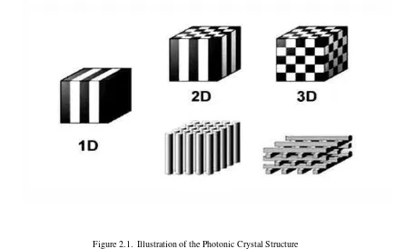
Page Figure 2.1. Illustration of the Photonic Crystal Structure of Research ... 3 Figure 2.2. Field Distribution in the Defect inside the Photonic
Crystal ... 8 Figure 2.3. Profile of PBG in the Photonic Crystal Structure (a).PBG
for Photonic Crystal without Defect. (b) PPB that
happens inside PBG for Photonic Crystal with Defect ... 9 Figure 2.4. Structures of One Dimension Photonic Crystal with Two
Geometric Defects ... 9 Figure 2.5. Curve for One Dimension Photonic Crystal
Transmittance with Two Geometric Defects. (a) Changes in the Regulator’s Defect Cause the PPB Shiftment. (b) Changes in Defect 2 (Receptor) Cause the Maximum
Transmittance of PBB Decreased ... 10 Figure 2.6. The Relationship between Defect’s Refractive Index and
the Transmitance of Photonic Pass Band that was Used
for Refractive Index Sensor ... 10 Figure 2.7. One Dimension Photonic Crystal Model with M = 4, N =
6 and L =2 ... 11 Figure 2.8. Illustration of the Sensor Device that is Photonic
Crystal-Based to Detect a Solution’s Concentration ... 12 Figure 3.1. Design of Photonic Crystal Arrangement M + L = N ... 13 Figure 3.2. The Simulation of the Refractive Index Changes’ Effect
in Defect-2 toward the Photonic Crystal Transmittance
Changes ... 13 Figure 3.3. The Equipments that was Used for Fabrication of
Photonic Crystal ... 14 Figure 3.4. Schematic Diagram for Characterization and Sensing
Test ... 15 Figure 3.5. Illustration of devices of photonic crystal-based sensors
for detecting the concentration of solution ... 16 Figure 4.1. (A) Transmittance Response (PPB) that were Influenced
by Variations of Refractive Index in the Second Defect. (B) The Relationship between PPB Transmittance
Figure 4.3. The equipment that used for optical characterization and
sensing testing of photonic crystal ... 18 Figure 4.4. Measurement Results of the Optical Characterization and
Sensing Test of Photonic Crystal ... 19 Figure 4.5. The design size of the sensor devices ... 19 Figure 4.6. Design of the sensor devices in three-dimensional
illustrations ... 20 Figure 4.7. Sensor devices fabricated with the techniques of lathe ... 20 Figure 4.8. Scheme for Device Performance Measurement ... 21 Figure 4.9. Electronic circuit for light source controlling and light
intensity detecting ... 22 Figure 4.10. The Relationship between Light Intensity (Volt) and
Sugar Solution Concentration (g/L) for Configuration
242 and 462 of the Photonic Crystal ... 23 Figure 4.11. A Linear Regression Analysis for the Measurement Data
with range of concentration : A. Between 20 and 100
g/L ; B. Between 100 and 200 g/L ... 23 Figure 4.12. Design of photonic crystal by using reflection method ... 24 Figure 4.13. Illustration design sensor devices by using reflection
method ... 25 Figure 4.14. The results of measurement of sugar solutions
concentration by using reflection method. A. Range of Concentration 20 - 500 g/L, B. 20 -100 g/L, C. 100 - 500
g/L ... 26 Figure 4.15. Alternative design sensor devices for various
applications ... 27 Figure 4.16. Reflection measurement of Substrate BK-7 before and
Appendix 1 : Process Program ... 35
Appendix 2 : 2D Design of Transmission Device ... 36
Appendix 3 : 2D Design of Transmission Device (Detail) ... 37
Appendix 4 : 3D Design of Transmission Device ... 38
Appendix 5 : 2D Design of Reflection Device ... 39
Appendix 6 : 3D Design of Reflection Device ... 40
Appendix 7 : 2D Design of Drop System Device ... 41
Appendix 8 : 2D Design of Drop System Device (Detail) ... 42
Appendix 9 : 3D Design of Drop System Device ... 43
LIST OF PUBLICATION
Page [1] Design and Fabrication of One-Dimensional Photonic Crystal Based Optical Sensor ... 42[2] Desain Dan Fabrikasi Sensor Real Time Berbasis Kristal Fotonik Satu Dimensi Untuk Deteksi Konsentrasi Larutan Gula ... 43
CHAPTER I
INTRODUCTION
1.1. Background
Photonics is a field of study that observes the interaction of light with the material that becomes the key of technology in the 21st century. The relationship between photonic and nanotechnology is relatively close. The photonic technology plays vital roles in the development of communication and information technology, lightning, manufacturing and life sciences. Photonics stimulates technology innovations and device production creativity. Moreover, photonic technology has influenced the development of data capacity in the telecommunication networks. This technology develops incredibly fast, and in order to maintain this condition, strong industries are needed. In order to develop this photonic technology, it needs many innovations, whether it is in theory or technology. In daily life, without realizing it, humans have taken the benefits of photonic, such as the usage of cell phones, CD, laser, and others. Therefore, it needs public relations to introduce this photonic field to the society.
Numerical studies toward one dimension of photonic crystal with two defects showed that the position of photonic pass-band (PPB) in the photonic band-gap (PBG) could vary with respect to the changes of refractive index and the geometrical thickness in both defects. Those two defects, furthermore, will be called regulator and receptor, each of them will show special function of its own. The effect of changing the regulator causes the changes in frequency or wavelength transmitted by EM waves that went through the photonic crystal. The effect of changing the receptor, however, can cause changes in peaks of the transmittances. Therefore, it will allow the development of a device that can manipulate the changes in the defect layer and utilize the response changes.
this refractive index are conducted by making a defect from sugar solution with various concentrations. The purpose is to make the photonic crystal able to be used as a sensitive sensor for the varying concentration in the sugar solution. In accordance with this, an adequate device or measuring tool for this purpose will be built. The aim for this research is to create a measuring tool for sugar solution that is accurate, sensitive, and able to measure fast and real time.
1.2. Purpose of the Research
The purpose of this research is to design and fabricate a photonic crystal based sensor for sugar solution’s concentrations. In order to do the design, the Film Star Software is use to simulate the fabricated photonic crystal prior fabrication. The photonic crystal is further synthesized by using electron beam evaporation method in nanometer order with a high standard precision optical process. The performance of sensing capability of photonic crystal is tested by
using VIS-NIR spectroscopy method in a real time test mode.
1.3. Scope of the Research
CHAPTER II
THEORETICAL BACKGROUND
2.1. Light Propagation inside the Photonic Crystal
The first person that studies the one dimension photonic crystal is Lord Rayleigh in 1887. He showed that the light propagation depend on the forbidden angle for a certain range of frequency. Many optoelectronic devices use one dimension photonic crystal as a frequency filter or dielectric mirror. When the light hits the layer, each surface reflects a part of the field. If we choose the thickness of each layer for a suitable value, the reflected field will combine a constructive phase, producing constructive interference and strong reflectance called Bragg Reflection. It is shown that the Bragg Reflection in the periodical dielectric structure create a photonic band gap (PBG). When the periodicity destroyed by the present of defects in the photonic crystal, the localization of the defect mode will appear inside the PBG due to of the changes in light interference.
As discussed in the previous chapter, the search of the best way to control the light propagation always becomes the main priority. The main concern of this research focused on the interaction between the electromagnetic field with solid-like-structure photonic crystal. The Maxwell Equation is the first and definitely the most important one in this theory. The first step is to derivate all the formula in the Maxwell Equation. The components in the electromagnetic wave, electric field and magnetic field will move through a medium that is load free and the free wave has been connected through 4 Maxwell Equation, as follows;
) , ( )
,
( B r t
t t r E (1) ) , ( ) , ( ) ,
( D r t J r t
t t r
H
(2) 0 ) , (
B r t (3)
) , ( ) ,
(r t r t D
(4)
The standard notation for electric field (E), magnetic field (H), electricity propagation (D), and magnetic induction (B) have been used in this equation. Remembering again a certain identity from the vector arithmetic:
2 ( )A ( . )A A
(5)
and adjust it with the Maxwell Equation, where . ( ) 0 r and ( ) 1r
2 2
0 0 2
E E t (6) 2 2
0 0 2
H H t (7)
The equations are the equation of standard wave that has many solutions, one of which is the equation for an area with the shape of ( . )
0
i k r t
( . ) 0
i k r t
H H e , where the wave’s vector and frequency are shown by k and ω simultaneously. Furthermore, the equation for wave produces:
2 1
[ ( , )] ( , )
( )r E r t c E r t
(8)
2 1
[ ( , )] ( , )
( )r H r t c H r t
(9)
The equations above usually called as master equation by the researchers
in photonic crystal. Although it does not show something new from the perspective of the researchers, the test by using Schrodinger’s Eigen-value equation that is more familiar in the quantum mechanics has opened a new point of view. Object with mass m obey the Schrodinger equation, and its energy can be calculated through the corresponding equation. Therefore, the equation for electric field or magnetic field has an analogy with Schrodinger’s [4] wave equation.
One of the general solutions for equation (8) is monochromatic harmonic plain wave that depends on time
,
i tE r t E r e that is reinserted into equation (9), producing EM wave in the frequency domain of
2 2
,
0 k E r
(10) In the cartesian coordinate system, equation (10) reduced into three scalar equations for each electric field components Ez, Ex, and Ey. This equation can be
solved through separation of variables method. For the TE wave, electric field E = (0, Ex, 0) is linearly polarized in the y direction and described in the form of
scalar function Ey (z, y), so it produces:
,
ik yyE z y E z e (11)
i k z(z t) i k z(z t)
ik yy E Ae Be e(12)
2.2. Modeling and Mathematical Formulation
Matrix method is the best way to perform an accurate analysis of the EM wave transmission in a layered medium. Generally, matrix formalism is used to relate electric field and magnetic field components in each layer [8]. We use the standard transfer matrix method to observe TE and TM wave’s transmittance. The advantage of this transfer matrix method is that it gives the exact numeric solution from the model made and is relatively easier modified if the structure of the model needs to be changed. The field in the last layer of the photonic crystal for both refractive polarizations can be calculated from the following relation:
( ) / 1 / 0 i t TE TM r t E E E E
(13)
where Ei, Er and Et are electric fields that came, reflected, and transmitted and
matrix: �= 0−1
1 1− 1
2 2− 1
�1 �1 −1
1 1− 1
1 1− 1
2 2− 1
�2 �2 −1
2 2− 1
1 1− 1
2 2−
1 (14)
is a transfer matrix where matrix Piand Qi for TE and TM polarizations are given
by:
1 1
cos cos
TE i
i i i i
P
k k
, and
1 1 1 1 cos cos cos cos cos cos i i i i i i i i
ik d ik d
TE
j ik d ik d
i i i i
e e
Q
k e k e
cos i cos i
TM i i i P k k
, and
1 1
1 1
cos cos
cos cos
cos i i cos i i
i i
i i
ik d ik d
i i
TM
j ik d ik d
i i
e e
Q
k e k e
with ki = niω/c, i = 0, 1, 2 for fixed structures, meanwhile kd1 = nd1ω/c, kd2 =
nd2ω/c, are for defect layers, θi shows the coming angle in each layer. The
transmittance of the electric field is given below:
2 2
/
t i
T E E
(16)
2.3. The Condition of Quarter-Wave Stack
The thickness of each medium layer (n1 and n2) can be chosen to fulfill the
quarter-wave stack condition, that is: 1 = � 4 1
and 2 = � 4 2
so both layers have the same optic length (n1d1 = n2d2). M o r e o v e r , � is called the operational
wavelength and is the centre of the first PBG frequency that is formed (for m=l), equation:
�� = 2 (17)
where neff is the effective refractive index that can be stated as:
= 1 1+ 2 2 (18)
and Lis the crystal’s periods, which is d1+ d2, meanwhile � is usually stated in
a frequency form
� =2�
� =
� 2 1 1
= �
2 2 2
(19)
and if it is compared with Bragg, for n1d1 = n2d2 and neff , and defined in
equation (3), the Bragg frequency can be simplified into:
���� = 2 1�1
= �
2 2 2
(20)
so from the equation we can get
Bragg = mo (21)
2.4. Fields Distribution inside the Defect Layer
In the photonic crystal with imperfectly periodicity, there will be a resonance mode in the PBG range where EM wave frequency that exists is the
same as the frequency of the imperfect mode of the crystal. The wave with the imperfect mode or frequency will be reflected simultaneously in harmony (back andforth) around the imperfect mode by DBR (distributed Bragg reflector) in the
left and right sides of the imperfect layer that functioned as PBG mirror. This causes the photons to localize around the imperfects and cause high field enhancement. Field enhancement in the defect area leads to a full transmittance in
the PBG in its resonance frequency, which is usually defect mode.
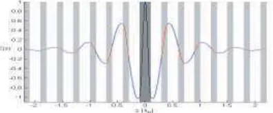
Figure 2.2. Field Distribution in the Defect inside the Photonic Crystal
The EM field’s profile which is propagating inside the photonic crystal layer can be described by using the transfer matrix method and by considering the translation’s symmetry. The solution for the EM field that comes in the z direction which is vertical with the crystal layer and move in layer n1 and n2 can be written
as:
1 1
1 1
( ) ik z ik z
E z A ie B e (22)
2( 1) 2( 1)
2 2
( ) ik z d ik z d
E z A ie B e (23)
2.5. Transmittance of Photonic Pass Band in the Defect Cell
transmittance is known as Photonic Pass Band (PPB) that is located inside the
PBG that should be a forbidden area for the periodic crystal structure. The existence of defect inside this photonic crystal is analog with the existence of impurity inside the material structure of a semiconductor.
Figure 2.3. Profile of PBG in the Photonic Crystal Structure (a).PBG for Photonic Crystal without Defect. (b) PPB that happens inside PBG for Photonic Crystal with Defect
2.6. One Dimension Photonic Crystal with Two Defects
One dimension photonic crystal with two defects has a more interesting phenomenon. The structure of one dimension photonic crystal with two geometric asymmetric defects is illustrated in the Figure 2.4. below:
Figure 2.5. Curve for One Dimension Photonic Crystal Transmittance with Two
Geometric Defects. (a) Changes in the Regulator’s Defect Cause the PPB Shiftment. (b) Changes in Defect 2 (Receptor) Cause the Maximum Transmittance of PBB Decreased (H. Alatas, 2006)
The structural different between the one dimensional photonic crystal with two asymmetric defects and one dimensional photonic crystal with one defect is that in the former structure, the refractive index in the left corner of the crystal is not the same with the refractive index in the right corner of the crystal. PPB that used to form in the photonic crystal with two asymmetric geometric defects has the same response toward the changes in defect width (dD2).
2.7. Photonic Crystal Model for Optical Biosensor
One dimensional Photonic crystal model that we made consists of a fixed layer of dielectric layer that criss-crossed along with two defect layers, they are:
n0 ns(n1/ n2 )M D1 (n1/ n2 )N D2 (n1/ n2 )L ns n0 , like the structure described in
Figure 4.1.1. n1 and n2 showed the refractive index in the fixed layer (n1/ n2 ) and
its thickness is is marked by (d1/ d2 ). Two defect layers were marked by (D1) ≡
(nd1/ n2), and (D2) ≡ (nd2/ n2) that were related with its thickness (dd1/ d2) and (dd2/
d2) simultaneously. The refractive index of the substrate and background medium
are ns and n0 respectively.
Figure 2.7. One Dimension Photonic Crystal Model with M = 4, N = 6 and L =2.
The total number of cell layers in the left side of D1, between D1 and D2
also after D2, is given by M, L, and N, in orders. In the numerical studies, we
assumed that the materials used have low capability to absorb the TM wave ( low-loss media). The parameter used are given by n0 = 1 (air), ns = 1.52(BK7), n1 =
2.1 (OS-5), n2 = 1.38 (MgF2) and the optical thickness fulfills the quarter wave
stack condition: 525 nm. First defect of cell is made by dd1 = λ0/2, whereas the
second one is made empty space to insert the sugar solution as sensing material.
2.8. Sensor Device
In the last year, several applications of biosensor were already exist and based on the characteristics of transmission spectrum and reflection in the surface of the object. The Surface Plasmon Resonance (SPR) sensor has been used widely
for screening the biochemistry interactions, while other researcher groups
silicon or guided mode resonance reflectance filters. Other application used the
optical resonance shiftment to test the DNA.
The unique characteristics of the PPB is that it is not only used as a filter but also can be developed as an optical sensor related to the function of defect, one of which is as a regulator and the other is as a receptor. A type of an optical sensor that can be developed is the refractive index sensor that can measure the substance concentration in a solution, such as sugar solution sensor or salt concentration. As an example, the refractive index of the sugar solution for a 30% concentration is 1.37, meanwhile for a 50% concentration, the refractive index is 1.42.
To develop a biosensor, a photonic crystal can be used so that it produces a narrow resonance mode where the wavelength is very sensitive toward the modulation that is inducted by the biochemistry material deposition in the defect layer. A structure of sensor consists of a transparent material that has low refractive index with the periodic surface structure coated with a thin layer that has high index.
Figure 2.8. Illustration of the Sensor Device that is Photonic Crystal-Based to Detect a
Solution’s Concentration
SOLUTION
CHAPTER III
RESEARCH METHODOLOGY
3.1. Modeling and Simulation
Prior to the fabrication, we do a simulation by using FilmStar Software. Photonic Crystal for a pattern of N = 2, L = 4 and M = 2, with one defect as a fixed regulator and one defect change in the receptor. The refractive index of the material used is OS-5, with an refractive index 2.1, and also MgF2 with the
refractive index of 1.38 - a product from Soltex Co. Ltd., each of which plays its role as a High Index and Low Index.
The Figure 3.1 below is the arrangement of photonic crystal design and the simulation results.
Figure 3.1. Design of Photonic Crystal Arrangement M + L = N
3.2. Fabrication Process
After the simulation, the design is implemented in the coating machine for fabrication, which is conducted at PT. Nagata Opto Indonesia. This process is carried out by using electron beam evaporation method in the Optorun Gener -
1300 machine. The pressure of the vacuum room = 1.0x10⁻³ Pa and the temperature = 300 oC (573 K).
Further, the coating process is performed in two steps. First, coating 22 layers from layer-1 until layer-22 before the second defect. In this first process, the first defect in layer-9 is already included. This process is implemented in substrate-1 that is in the form of glass BK-7 (refractive index = 1.52). Second, coating 5 layers from layer-28 until layer-24, meanwhile layer-23 is emptied to place the sugar solution that will be further analyzed. This process is implemented in substrate-2 that is also in form of glass BK-7 (refractive index = 1.52).
3.3. Optical Characterization
Characterization is carried out by using the Spectrophotometer Olympus USPM method to test the compatibility of the fabrication result with the simulation result and by using Spectrophotometer UV-VIS Ocean Optics USB 1000 to measure the photonic crystal’s transmittance with the defect’s refractive index of the receptor. The following is the scheme for the implementation of the experiments where sample of sugar solution with the concentration of 20, 40, 60, 80 and 100 g/L is given in the defect.
Figure 3.4. Schematic Diagram for Characterization and Sensing Test
3.4. Device Realization
Device realization is conducted by considering several aspects, they are the photonic crystal design, selecting the light sources that will be used, selecting the photodetector, operational amplifier, and instrumentation system.
The design of the photonic crystal is based on simulation result and fabrication is targeted with the centre in PPB in the value of 525 nm by considering the light source that probably used based on the existing reference. The desired design is easily gotten through the simulation by using FilmStar Software, but in the fabrication process there had to be an arrangement of the machine condition so the desired value can be obtained. To ensure this, quality test is prerformed as illustrated in Figure 3.5.
namely LED, had the wavelength of 525 nm as a specification. Similarly, detector is selected when one is going to detect photon that ranges of wavelength.
Figure 3.5. Illustration of devices of photonic crystal-based sensors for detecting the concentration of solution
CHAPTER IV
RESULT AND DISCUSSION
4.1. Numeric Simulation Results
Numeric simulation is carried out by configuring the design of photonic crystal 462 and 242 as a comparison (see Figure 4.1). Such an action is to find the formation process of the PPB phenomenon predicted by previous publications and to show the influence of the number of photonic crystal cell units toward the sensitivity of the device that will be created, so it can give the description for the next development.
Figure 4.1. (A) Transmittance Response (PPB) that were Influenced by Variations of Refractive Index in the Second Defect. (B) The Relationship between PPB Transmittance toward the Refractive Index (TP Negara, 2009)
Figure 4.2. Profile of Field Intensity in the Photonic Crystal for the Configuration of 2-4-2 and 4-6-2 (TP Negara, 2009)
intensity in the defect layer enabled a field to go out of the defect layer and formed enhanced intensity of the new field in the next defect layer, depending on the system configuration and the refractive index value in each defect layers. For system 2-4-2, it seems that an enhancement of field in the first defect produced a new resonance in the second defect.
4.2. Characterization and Sensing Test
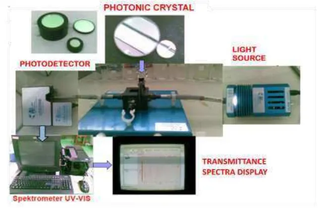
[image:31.595.144.467.384.594.2]The optical characterization and sensing performance conducted to the fabricated photonic crystal by making a spacer with a distance of 2 mm to be filled with sugar solution inside the photonic crystal system before it is made in the form of optical sensor device. The measurement is carried out by using Ocean Optics Spectrophotometer UV Vis USB 2000. The sugar solution used in this test is made with the concentration of 20, 40, 60, 80 and 100 g/L. The measurement is carried out as shown in Figure 4.3 below:
Figure 4.3. The equipment that used for optical characterization and sensing testing of photonic crystal
Figure 4.4. Measurement Results of the Optical Characterization and Sensing Test of Photonic Crystal
4.3. Design and Realization of the Sensor Devices
Before making the sensor devices is the design by using AutoCAD 2009 software. This step is performed to obtain a precision devices and has a standardized form that can be done if the mass production in time to come. Figure 4.5. below shows the complete two-dimensional image with a size devices that will be made.
[image:32.595.157.459.461.660.2]To provide a clearer illustration in Figure 4.6. for the manufacture of sensor devices made complete three-dimensional design for all parts are required, making it easier manufacturing techniques.
Figure 4.6. Design of the sensor devices in three-dimensional illustrations.
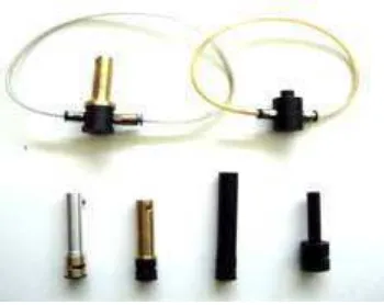
By considering the above design, the sensor devices are made with material POM (Polyoxymetilene), a plastic material readily available on the market. But this material can be replaced by other materials in accordance with field conditions and the sensing material that will be measured. The following Figure 4.7. shows the results of sensor devices fabricated by using lathe techniques:
Figure 4.7. Sensor devices fabricated with the techniques of lathe.
4.4. Device Performance Measurement
The measuring technique is carried out by making a 500g/L of sugar solution as much as 100 mL, and then this solution is poured inside a goblet to be measured. This goblet is placed on top of a magnetic stirer to ensure that the
measurement of the sugar solution is in a homogen condition. The measurement for a lower concentration is conducted by adding into the solution in a certain amount until the solution’s concentration can be measured, and then the measurement can directly be conducted in the voltmeter screen. The recording of measuring results is performed when the solution can already be stated as homogen.
Figure 4.8. Scheme for Device Performance Measurement
From the measurement, the relationship curve between the light intensity measured by photodetector that is seen in the voltmeter (V) screen toward the
concentration of the sugar solution (g/L) can be made. This measurement result showed the same phenomenon with the simulation result and sensing test in the early step of test, therefore, this result can be considered to be consistent.
lightening and light detection received by the photo detector is controlled by the electric circuit depicted in Fig. 4.9.
Figure. 4.9. Electronic circuit for light source controlling and light intensity detecting.
From the electrical circuit in Figure 4.6, the intensity of the light source can be altered by using the variable resistor VR1, so that the required light for the LDR during detection can be adjusted. Meanwhile, the variable resistor VR2 can be applied for measurement system calibration as well as adjustment of the measurement value upon the reference solution. For the measurement stability a voltage follower in both measurement points and a signal amplifier in the form of differential operational amplifier are installed. Measurement is carried out using a simple voltmeter with amplification according to the following equation (24)
� = − 4
3
. �2− �1 (24)
where R3 = R5 dan R4 = R6.
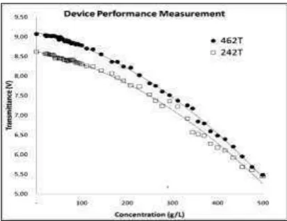
Figure 4.10. The Relationship between Light Intensity (Volt) and Sugar Solution’s Concentration (g/L) for Configuration 242 and 462 of the Photonic Crystal
The results of these measurement are not linear that caused by electronic part and mechanism in electronic circuit system, so we can approach these curves by polinomial regression. These curves can be used to calculated measurement data for application in several field. This calculation is easy for automatic digitalized or computerized measurement, but for simpler calculation we have to use a linear regression approach.
In order to conduct a linear regression analysis, the curve in Figure 4.10 is divided into two linear areas: the one with the concentration that ranges from 20 – 100 g/L and the other one with the concentration that ranges from 100 – 500 g/L. The result from the linear regression analysis can be seen in Figure 4.11A and 4.11B.
From Figure 4.11, the linear regression analysis results toward the photonic crystal configuration of 242, it is found that the sensitivity is 7.6 mV/ (g/L) and the determination coefficient is 97.85% for the concentration 100 – 500 g/L. Meanwhile in the range of 20 – 100 g/L, it is found that the sensitivity is 3.2 mV/ (g/L) and the determination coefficient is 93.35%.
For the photonic crystal with the configuration 462, it showed that the sensitivity is 8.2 mV/ (g/L) with the determination coefficient of 98.50% for the concentration range of 100 – 500 g/L. Meanwhile, in the range of 20 – 100 g/L, the sensitivity of the photonic crystal is 3.5 mV/ (g/L) with the determination coefficient of 93.46%.
If we compare the sensitivity value and the determination coefficient from each photonic crystal’s configuration, it can be stated that the configuration 462 is relatively better than configuration 242.
4.5. Alternative Design
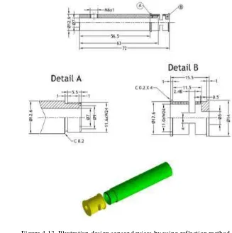
In this study is conducted development of sensor mechanism to increase sensitivity factor of devices. If before the sensor is made by using light transmission, made possible by the reflection method in the hope of having a higher sensitivity because the light will pass through the photonic crystal system twice in the forward and backward direction.
This development requires the reflector at the end of the photonic crystal system. This is conducted by adding a layer 100 nm thick aluminum as reflector and an added layer MgF2 as protector coating because aluminium layer is very
easily scratches if it exposed.
Because there are changes in measurement methods, the mathematical formulation used should be modified as the illustration shown in below equation:
(25)
(26)
[image:38.595.133.460.377.706.2]Then do the same thing in the design of the sensor devices. The following image shows the design tool in the form of two and three dimensions.
The advantage of sensor devices with a design method is a form of reflection that are simpler and smaller (compact) and can be used in the measurements with a high risk because this device does not include electronic devices in it, so secure in the measurement of flammable materials such as the measurement of alcohol levels, the octane in the fuel and others. Shortcomings, this device requires a tool with a Y junction fiber optic or a beam spliter to separate the light coming from the light source and reflected light that is detected by photodetector. However, it is still tolerable because for applications with a higher sensitivity level and the security level, so that is still competitive for specific applications, especially for the needs of industry.
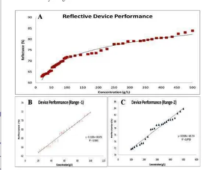
[image:39.595.93.505.354.700.2]The next testing sensor devices with reflection method to prove that this method has a higher sensitivity. Figure 4.14 below are the results of measurements by using the reflection method.
In Figure 4.14 A, we can see that the curve of measurement data is appoached by polinomial regression. The result is not linear. This result is influented by electronic circuit system and part that used in the apparatus. So, we can simplify calculation by using linear regression analysis. Here, we have to devide the curve become two linear region i.e. between 20 and 100 g/L and between 100 and 500 g/L, see in Figure 4.14A and 4.14B. This approach result sensitivity of sensor is 0.1138 %/(g/L) and determination coeficient is 98.45% for range of concentration between 20 and 100 g/L, and for range between 100 and 500 g/L, senstivity of sensor is 0.0306%/(g/L) and coeficient determination is 97.09%.
If we compared the results of measurements data from transmission method and reflection method in Figure 4.4 and 4.14B, we can see that device with reflection method show better results. In the transmission method shown sensitivity from the gradient of linear regression curve of 0.0585% / (g / L), whereas the gradient method of reflection obtained linear regression curves of 0.1138% / (g / L). These results indicate that the sensitivity of the device with the reflection method has a greater sensitivity, almost double, if we compared with device with transmission method.
[image:40.595.223.398.571.710.2]By utilizing these two measurement methods mentioned above, the transmission and reflection, made various forms of sensors for various measurement needs in the field. Following a successful sensor devices are made for each application required.
4.6. Design Optimization
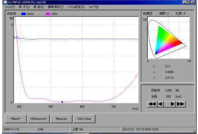
[image:41.595.145.479.251.477.2]Design optimization in the manufacture of optical sensors based on one-dimensional photonic crystal is to add antireflection coating on the glass substrate to anticipate a weakening of the light source will enter into the system of photonic crystal structures and light to be received by photodetector. The following figure is measured reflection curve glass substrate before and after the given antireflection layer.
Figure 4.16. Reflection measurement of Substrate BK-7 before and after giving antireflection coating layer.
CHAPTER V
CONCLUSION
5.1. Conclusion
This research shown that the prototype of one dimension photonic crystal with two defects could be implemented as optical sensor to measure a certain solution’s concentration. In this case, we used sugar solution with the concentration range from 20 - 500 g / L and the measured refractive index between 1.332 and 1.415 as a sample target. To analyze the result, we used the linear regression method. We divide the data into two linear areas: the first is the area with 20-100 g / L and , and second, the area with 100 - 500gr / L. The results shown that the determination coefficient could be reached up to 98%. Based on this fact, we are certain that this device can be used to measure the solution’s concentration in varieties of applications; for instance, to measure the water sanitation for the environment, blood sugar for medical field, sugar content in the baverage industries, and many others. This measurement can also be carried out by using the in situ and real time mechanism.
5.2. Future Work
REFERENCES
Alatas H et al. 2006. Single frequency refractive index sensing based on finite
one-dimensional photonic crystal with two defect. Jpn J Appl Phy. 45(8B):6754-6758.
Alaydrus M, Dipojono HK, Alatas H. 2007. Dynamic simulation of gaussian beam propagation inside a photonic crystal based refractive index sensor by means of FDTD method. Proc. of Techno SIM . H1 – H5.
Deych LI. 2005. One-dimensional photonic crystals based on periodic multiple quantum well structures. Phys. stat. sol. 2(2):805–808.
Hardhienata H et al. 2006. Photonic pass band characteristic of a finite one dimensional photonic crystal with two defects at omnidirectional light incident. Proc. Of ICMNS : 907 – 910.
Hasek T. 2006. Photonic crystals for fluid sensing in the subterahertz range. American Institute of Physics. Appl Phy Letters. 89:501-508
Mingaleev SF. 2004. Tunable photonic crystal circuits: concepts and designs based on single-pore infiltration. Optics Letters. 29(24): 245-252
Mayditia, H. etal. 2005. Analysis of one dimensional photonic crystals with defect and asymmetric edges for sensor application. Proc of ICICI 740 –
744.
Nasilowski, Tomazs. 2006. Metrological application of photonic crystal fibres.
Proceedings of the Symposium on Photonics Technologies for 7th Framework Program Wroclaw. Belgium.
Negara T.P. 2009. Study of electromagnetic wave propagation in 1D photonic crystal with three defect and its application for optical biosensor. [Thesis]. Biophysics Graduate School, Bogor Agricultural University. Indonesia. Özbay, E., B. Temelkuran. 1996. Reflection properties and defect formation in
photonic crystals. Appl. Phys. Lett. 69(6):157-169.
Painter, Oskar, Kartik Srinivasan. 2002. Polarization properties of dipolelike defect modes in photonic crystal nanocavities. Optics Letters
27(5):489-495
Rahmat M. et al. 2009. Real-Time Optical Sensor Based on One Dimensional Photonic Crystals with Defects. Proceedings of the International Conference On Information, Communications, Instrumentation and Biomedical Engineering. Bandung 23-24 November 2009.
MAMAT RAHMAT. Design and fabrication of one-dimensional photonic crystal as a real time optical sensor for sugar solution concentration detection. Supervised by HUSIN ALATAS, dan IRMANSYAH
A previous theoretical study of a finite one-dimensional photonic crystal composed of 12 unit cells with two defects had shown the existence of Photonic Pass Band (PPB) inside the Stop Band, which was suggested as a useful refractive index sensor due to the sensitive variation of PPB with respect to the change of refractive index of either defect layer material. We report in this presentation our successful fabrication of a prototype of this system by means of electron beam evaporation equipment in a sample chamber at pressure of 10-3 Pa with BK-7 glass substrate at temperature 573 K. Each of the photonic cells is composed of a high index layer of OS-5 with refractive index of n2.10, and an equal optical
thickness low index layer of MgF2 with n1.38. In the first defect cell, the high
index layer has twice the thickness of the other layers with the low index layer left unchanged, while in the second defect cell separated by 6 unit cells, the first layer is void to be filled with the sample solution. The device was used for measuring the refractive index of sugar solution with concentration range of 20-100 g/L in the real time mode. The result was found to achieve determination coefficient up to 98%. Further measurement performed has demonstrated a result in good agreement with theoretical prediction reported previously.
MAMAT RAHMAT. Design and fabrication of one-dimensional photonic crystal as a real time optical sensor for sugar solution concentration detection. Supervised by HUSIN ALATAS, dan IRMANSYAH
This study is developed from the results of theoretical study of one-dimensional photonic crystals with two defects that have unique characteristics in response of Photonic Band Pass (PPB) on the frequency interval of Photonic Band Gap (PBG). This study focused on prototyping photonic crystal sensor based on refractive index changes in a second defect that serves as a receptor in which to respond transmitansi value changes, so that could be used as a single-frequency index sensing. The reference wavelength that used in this study is 525 nm.
This research was conducted with some of the following stages: theoretical model of observation through implementation and simulation, fabrication of photonic crystal, characterization, sensing test, assembly and instrumentation devices, and device performance measurement. Fabrication process of a prototype of this system by means of electron beam evaporation equipment in a sample chamber at pressure of 10-3 Pa with BK-7 glass substrate at temperature 573 K. Each of the photonic cells is composed of a high index layer of OS-5 with refractive index of n2.10, and an equal optical thickness low index layer of
MgF2 with n1.38. In the first defect cell, the high index layer has twice the
thickness of the other layers with the low index layer left unchanged, while in the second defect cell separated by 6 unit cells, the first layer is void to be filled with the sample solution.
This research shown that the prototype of one-dimension photonic crystal with two defects could be implemented as an optical sensor to measure a certain solution's concentration. In this case, we used sugar solution with the concentration range from 20 to 500 g / L and the measured refractive index between 1.332 and 1.415 as a sample target. To analyze the result, we used the linear regression method. We divide the data into a linear two areas: the first is the area with 20-100 g / L and, and second, the area with 100 - 500gr / L. The results shown that the determination coefficient could be reached up to 98%. Based on this fact, we are certain that this device can be used to measure the solution's concentration in varieties of applications; for instance, to measure the water sanitation for the environment, blood sugar for medical fields, sugar content in the baverage industries, and many others. This measurement can also be carried out by using the in situ and real-time mechanism.
CHAPTER I
INTRODUCTION
1.1. Background
Photonics is a field of study that observes the interaction of light with the material that becomes the key of technology in the 21st century. The relationship between photonic and nanotechnology is relatively close. The photonic technology plays vital roles in the development of communication and information technology, lightning, manufacturing and life sciences. Photonics stimulates technology innovations and device production creativity. Moreover, photonic technology has influenced the development of data capacity in the telecommunication networks. This technology develops incredibly fast, and in order to maintain this condition, strong industries are needed. In order to develop this photonic technology, it needs many innovations, whether it is in theory or technology. In daily life, without realizing it, humans have taken the benefits of photonic, such as the usage of cell phones, CD, laser, and others. Therefore, it needs public relations to introduce this photonic field to the society.
Numerical studies toward one dimension of photonic crystal with two defects showed that the position of photonic pass-band (PPB) in the photonic band-gap (PBG) could vary with respect to the changes of refractive index and the geometrical thickness in both defects. Those two defects, furthermore, will be called regulator and receptor, each of them will show special function of its own. The effect of changing the regulator causes the changes in frequency or wavelength transmitted by EM waves that went through the photonic crystal. The effect of changing the receptor, however, can cause changes in peaks of the transmittances. Therefore, it will allow the development of a device that can manipulate the changes in the defect layer and utilize the response changes.
this refractive index are conducted by making a defect from sugar solution with various concentrations. The purpose is to make the photonic crystal able to be used as a sensitive sensor for the varying concentration in the sugar solution. In accordance with this, an adequate device or measuring tool for this purpose will be built. The aim for this research is to create a measuring tool for sugar solution that is accurate, sensitive, and able to measure fast and real time.
1.2. Purpose of the Research
The purpose of this research is to design and fabricate a photonic crystal based sensor for sugar solution’s concentrations. In order to do the design, the Film Star Software is use to simulate the fabricated photonic crystal prior fabrication. The photonic crystal is further synthesized by using electron beam evaporation method in nanometer order with a high standard precision optical process. The performance of sensing capability of photonic crystal is tested by
using VIS-NIR spectroscopy method in a real time test mode.
1.3. Scope of the Research
CHAPTER II
THEORETICAL BACKGROUND
2.1. Light Propagation inside the Photonic Crystal
[image:102.595.96.531.450.724.2]The first person that studies the one dimension photonic crystal is Lord Rayleigh in 1887. He showed that the light propagation depend on the forbidden angle for a certain range of frequency. Many optoelectronic devices use one dimension photonic crystal as a frequency filter or dielectric mirror. When the light hits the layer, each surface reflects a part of the field. If we choose the thickness of each layer for a suitable value, the reflected field will combine a constructive phase, producing constructive interference and strong reflectance called Bragg Reflection. It is shown that the Bragg Reflection in the periodical dielectric structure create a photonic band gap (PBG). When the periodicity destroyed by the present of defects in the photonic crystal, the localization of the defect mode will appear inside the PBG due to of the changes in light interference.
As discussed in the previous chapter, the search of the best way to control the light propagation always becomes the main priority. The main concern of this research focused on the interaction between the electromagnetic field with solid-like-structure photonic crystal. The Maxwell Equation is the first and definitely the most important one in this theory. The first step is to derivate all the formula in the Maxwell Equation. The components in the electromagnetic wave, electric field and magnetic field will move through a medium that is load free and the free wave has been connected through 4 Maxwell Equation, as follows;
) , ( )
,
( B r t
t t r E (1) ) , ( ) , ( ) ,
( D r t J r t
t t r
H
(2) 0 ) , (
B r t (3)
) , ( ) ,
(r t r t D
(4)
The standard notation for electric field (E), magnetic field (H), electricity propagation (D), and magnetic induction (B) have been used in this equation. Remembering again a certain identity from the vector arithmetic:
2 ( )A ( . )A A
(5)
and adjust it with the Maxwell Equation, where . ( ) 0 r and ( ) 1r
2 2
0 0 2
E E t (6) 2 2
0 0 2
H H t (7)
The equations are the equation of standard wave that has many solutions, one of which is the equation for an area with the shape of ( . )
0
i k r t
( . ) 0
i k r t
H H e , where the wave’s vector and frequency are shown by k and ω simultaneously. Furthermore, the equation for wave produces:
2 1
[ ( , )] ( , )
( )r E r t c E r t
(8)
2 1
[ ( , )] ( , )
( )r H r t c H r t
(9)
The equations above usually called as master equation by the researchers
in photonic crystal. Although it does not show something new from the perspective of the researchers, the test by using Schrodinger’s Eigen-value equation that is more familiar in the quantum mechanics has opened a new point of view. Object with mass m obey the Schrodinger equation, and its energy can be calculated through the corresponding equation. Therefore, the equation for electric field or magnetic field has an analogy with Schrodinger’s [4] wave equation.
One of the general solutions for equation (8) is monochromatic harmonic plain wave that depends on time
,
i tE r t E r e that is reinserted into equation (9), producing EM wave in the frequency domain of
2 2
,
0 k E r
(10) In the cartesian coordinate system, equation (10) reduced into three scalar equations for each electric field components Ez, Ex, and Ey. This equation can be
solved through separation of variables method. For the TE wave, electric field E = (0, Ex, 0) is linearly polarized in the y direction and described in the form of
scalar function Ey (z, y), so it produces:
,
ik yyE z y E z e (11)
i k z(z t) i k z(z t)
ik yy E Ae Be e(12)
2.2. Modeling and Mathematical Formulation
Matrix method is the best way to perform an accurate analysis of the EM wave transmission in a layered medium. Generally, matrix formalism is used to relate electric field and magnetic field components in each layer [8]. We use the standard transfer matrix method to observe TE and TM wave’s transmittance. The advanta