DOI: 10.12928/TELKOMNIKA.v13i4.2362 1194
Modelling on Tracking Test Condition of Polymer
Nanocomposite using Finite Element Simulation
Fatin Liyana Muhamedin, MAM Piah and Nordiana Azlin Othman
Institute of High Voltage and High Current, Faculty of Electrical Engineering, UniversitiTeknologi Malaysia, 81310, UTM Johor Bahru, Johor, Malaysia
e-mail: [email protected]
Abstract
Electrical tracking is a formation process of a permanent conducting path across the insulating material due to surface erosion under high voltage stress. The existing of leakage current (LC) on the wet contaminated material surface causes the generation of surface discharges that resulted in the material degradation. The effects of electric field distribution and current density on LLDPE-Natural Rubber blends material were investigated using finite element method (FEM) analysis. In this paper, a variety of physical parameters particularly contaminant flow rate, various applied voltages, material properties of permittivity and conductivity were studied when nanofiller is added to LLDPE-Natural rubber blend. The simulation works using FEM software of Quickfield was applied to the tracking test condition of IEC 60587 standard. The results show that the electric field distributions are critical on the edges of contaminant solution path at higher voltage level. The current density and electric field distribution is increase with higher applied voltage. The polymer nanocomposite with 1-5 % of nanofiller exhibits a good resistance to tracking and erosion test.
Keywords: Finite Element Method, electric field, current density, surface discharges and, IEC 60587
Copyright © 2015 Universitas Ahmad Dahlan. All rights reserved.
1. Introduction
The wide usage of polymer as insulation materials in high voltage (HV) equipment has led to further investigation in their performances, mainly in term of electrical aspect. The aging of polymer due to environmental stresses can cause degradation of insulator polymer through surface tracking phenomena.Insulating surface are exposed to environmental stresses such as contaminant, UV ray stress, pollution and low severity fogconditions [1, 2]. Leakage current (LC) exists on the insulator surface when a certain voltage gradient is sufficient to cause the LC to flow under a wet contaminant condition.The continuous flow of LC will heat the insulator surfaceand the accumulated heat dissipation in narrow path on the insulator surface eventually formed a dry band arcing at the surface of the insulator. Dry band arcing occurs at the lowest surface resistance when non-uniform water layer is formed due to hydrophobicity loss. The hydrophobicity feature in the materials can reduce the onset of LC by increasing the failure time.Hydrophobicity loss could increase the development of LC and reduce the insulator resistance hence contribute in degradation [3]. Meanwhile, surface discharges occur when the air gap reached the critical flashover voltage across the dry band. Carbonized track and erosion will be formed when an arc burns the insulator material due to surface discharges. The carbonized track that developed pathway between two electrodes eventually will cause insulation failure to the system.
high electric field and when hydrophobicity ability of the material loss, the tendency of the surface insulator to degrade rise [13]. In the simulation analysis of electrical stresses on the surface of insulator,the investigation of electric field distribution around water droplet or water films are conducted by several researchers [14, 15]. Their result showsthat the contact angle of water droplet in the shed model which applied voltage is perpendicular to the insulator surface is neglected as the maximum strength of electric field are found to be appeared on top of the droplets [16]. However, the contact angle of water droplets affect the electric field distribution in the sheath model where voltage is appliedalong the insulator surface [17]. The maximum electric field is lowest when the distance between two water droplets reduce and increasing of a water droplet on the insulator surface [18]. When the contact angle of water droplet is low, it forms water layer on the insulator surface. In tracking and erosion resistance experiment, the contaminant solution layer are intended to be flown at certain flow rate on the insulator surface. This can initiate the dry band arcing when the contaminant layer is dry near the ground electrode when the voltage is supplied. Corona disharges emmision occured at the tips of the droplets whereas the dry band arcing occured during wet conditions and water droplets deformation affected the LC waveform obtained from the current density in the simulation [13].
The previous research in the field simulation is conducted mainly on the partial discharge, phenemona with a focus of the void and water droplet as the parameters [19, 20]. There is little attempt to investigate the field simulation in the inclined plane tracking test in related to surface tracking studies. Therefore, there is a possiblityto conduct this field work to encounter the correlation between the field simulation and actual experiment. If the approach of the field simulation in IPT test could forecast the result of the experiment of IPT test, then the field simulation work can be used as another option in investigating the surface tracking resistance. In this paper, the electric field, voltage and current density distribution are studied using Finite Element software on LLDPE-Natural Rubber materials with and without nanofiller. The analysis was conducted at various applied voltages under wet contaminant conditions. The simulation works were applied on the test configuration of IEC 60587 standard tracking and erosion test. The parameters used to investigate the electric field and current density distribution of insulator surface are applied voltage, electric conductivity and permittivities of insulating sample and contaminant solution.
2. Research Method 2.1. FEM Simulations
Bottom Electrode (Ground)
Top Electrode (HV) Filter-paper pad
under top electrode
Contaminant Test insulating
specimen
50 mm
Figure 1. Test specimen with the electrodes
To investigate the effect of contaminant on the insulator surface, two patterns of contaminant solution were drawn as depicted in Figure 2. Thispattern is chosen based on the picture of the contaminant solution along the insulator surface captured from the actual experiment. There are two patterns of contaminant solution flow are drawn in 2D in a plane parallel which are pattern A and Pattern B. Pattern A is the straight and narrow path of contaminant solution and the pattern B is bend and wide path of contaminant solution.An AC voltage supplied of 2.5, 3.5, 4.5 and 6.0 kV was applied to the insulating materials of LLDPE-Natural Rubber blends without nanofiller. The contaminant flow rate is adjusted according to the applied voltage as stated in IEC 60587 standard. The top electrode is connected to HV electrode while grounded at bottom electrode. In this study, only the insulating sample and electrode are considered while other accessories are neglected. Table 1 shows the applied voltage and contaminant flow rate according to IEC 60587 standard that used in the models.
(a) (b)
Figure 2. 2D parallel model of different patterns of contaminant solution, (a) Pattern A: straight and narrow path of contaminant solution and, (b) Pattern B: bend and wider path of
HV Electrode Sample
surface
Ground Electrode Path of
contaminant solution
Table 1. Test parameters [21]
Test voltage (kV) Preferred test voltage for method 1 (kV) Contaminant flow rate (ml/min)
1.0 to 1.75 - 0.075
2.0 to 2.75 2.5 0.15
3.0 to 3.75 3.5 0.30
4.0 to 4.75 4.5 0.60
5.0 to 6.0 - 0.90
It is important to state that the materials properties particularly electric conductivity, relative permittivity of the sample, contaminant solution and air are required for simulation purpose. In this study, the relative permittivity of the air was fixed to 1, the conductivity of the air is 2 x 10⁻⁴ Sm-1 [13] andthe relative permittivity of contaminant solution is 81 [14]. In the FEM simulation, the parameter used to vary the contaminant flow rate is the conductivity of contaminant solution. The conductivity of contaminant solution was varied correspondingly to the volume of contaminant solution based on contaminant flow rate as shown in Table 2. The volume of contaminant solution was obtained from each contaminant flow rate shown in Table 1 and the conductivity of contaminant was calculated by using equation (1). The resistance of contaminant solution is calculated using equation (2) by inserting the resistivity equal to
3.95 Ω. m as stated in IEC 60587 standard. The resistivity of each contaminant volume was calculated for the second time to obtain electric conductivity by using equation (2) and (1) respectively.
1
(1)l
R
A
(2)where
R
,
,landA
are the resistance, resistivity, length of contaminant solution and area of contaminant solution, respectively.Table 2. Electric conductivity of contaminant solution
Volume of contaminant (cm3) 0.15 0.30 0.60 0.90 Area of contaminant (cm2) 0.70 0.77 1.18 1.24
Resistance (kΩ) 65.83 32.92 16.46 10.97 Resistivity (Ω.m) 92.16 50.7 38.85 27.2 Conductivity (S/m) 0.011 0.020 0.026 0.037
2.2. Insulating Samples Properties
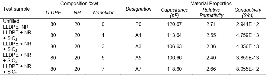
The formulated thermoplastic elastomer material composed of Linear Low-Density Polyethylene with Natural Rubber (LLDPE/NR) filled and unfilled with different percentage of silicone oxide (SiO2) is presented in this work. The conductivity of each composition was obtained from the conductivity analysis particularly polarization and depolarization current (PDC) measurement [22]. The capacitance value was obtained from measurement of sample using LCR meter between the upper and bottom electrode. Table 3 shows compound and designation of the samples with their material properties. For FEM simulation, the materials properties of conductivity and permittivity of sample material is required and the information can be obtained in Table 3. The conductivity of each sample was calculated using equation (3) and permittivity was calculated using equation (4).
( )
( )
r op dp
o o
i t
i
t
C U
where
o is free space dielectric constant ( 8.854 x 10⁻¹² F/m),C
o is capacitance of material,and
U
ois applied voltage (1000 V).r o
C
d
A
(4)where
o is free space dielectric constant ( 8.854 x 10⁻¹² F/m),C
is capacitance of material, dis thickness of sample material (1mm) and
A
is area of sample (50.27cm2 ).Table 3. Compound designation and material properties
Test sample
Composition %wt
Designation
Material Properties
LLDPE NR Nanofiller Capacitance (pF)
Relative Permittivity
Conductivity (S/m)
Unfilled
LLDPE+NR 80 20 0 P0 120.67 2.71 2.944E-12 LLDPE + NR
+ SiO2
80 20 1 A1 113.64 2.55 4.759E-13 LLDPE + NR
+ SiO2 80 20 3 A3 106.63 2.36 4.356E-13
LLDPE + NR + SiO2
80 20 5 A5 106.66 2.40 3.859E-13 LLDPE + NR
+ SiO2 80 20 7 A7 118.60 2.66 8.055E-12
3. Results and Analysis
3.1. Electric Field and Current Density Analysis
The problem type chosen in this work was AC conduction analysis to analyse the distribution of electric field caused by AC voltages in insulator materials. Variation of the field with respect to time is assumed to be sinusoidal. For AC conduction problems, the field simulator solves local and integral quantities is represented in the following equation:
i
0
U
(5)where, electric conductivity, σ and component of electric permittivity, εare constants within each block of the model. The complex vector of electric field intensity is calculated using equation 6;
d
E
gra U
(6)And equation for complex vector of active current density is expanded to
J
E (7)certain cross-sectional area of the contamination solution conducting film.The surface discharges are much related to the activity of the dry-band arcing that occurred in a certain region constantly causes by leakage current.Higher electric strength distribution appears at the narrow and edge shape of contaminant solution. At this region, the ionization process may be occurred as the electric field intensity is concentrated at the edges. The electric field distribution is more critical in the narrow path of the contaminant as shown in Figure 3 (a).
Strength E(105
V/m) RMS Magnitude
1.320
1.118
1.056
0.924
0.792
0.660
0.528
0.396
0.264
0.132
0.000
(a)
Voltage U( V)
RMS Value
2470
2223
1976
1729
1482
1235
988
741
494
247
0
(b)
Strength E(105
V/m) RMS Magnitude
1.740
1.566
1.392
1.218
1.044
0.870
0.696
0.522
0.348
0.174
0.000
(c)
Voltage
U( V)
RMS Value
2470
2223
1976
1729
1482
1235
988
741
494
247
0
(d)
Figure 3. (a) Electric field distribution for Pattern A, (b) Voltage distribution for Pattern A, (c) Electric field distribution for Pattern B, (d) Voltage distribution for Pattern B
measured from the HV electrode for narrow and straight contaminant path. It is noticed that for each applied voltage, highest value is observed in the narrow and straight contaminant path.For Pattern B, the maximum value of current density and electric field were found at a distance of 1.7 cm measured from the HV electrode. The maximum value recorded for current density for Pattern B are 0.066 A/cm2, 0.167A/cm2, 0.287A/cm2, and 0.537A/cm2 for 2.5 kV, 3.5 kV, 4.5 kV and 6.0 kV, respectively.The higher current density and electric field are recorded at the bending-shaped of contaminant flow for the bend and wide path of contaminant solution as depicted in Figure 4(b) and 5(b).
The results show that increasing in applied voltage causes an increase of both maximum current density and electric field. It is believed that higher applied voltage may give more energy for electron to get deposited on the solid insulator surface. The presence of this charge increases the surface conductivity and leads to the increasing of discharge magnitude. The large current density causes dry-band to be formed. This continuous process will develop arcing sparks and causes degradation process of the insulating surface called carbon track.
Distance from high voltage electrode to ground electrode (cm)
0 1 2 3 4 5
C u rr en t D ens it y ( A /c m 2) 0.0 0.1 0.2 0.3 0.4 0.5 0.6 0.7 2.5 kV 3.5 kV 4.5 kV 6.0 kV
(a) Distance from high voltage electrode to ground electrode (cm)
0 1 2 3 4 5
Cu rr e n t De n s it y ( A /c m 2) 0.0 0.1 0.2 0.3 0.4 0.5 0.6 2.5 kV 3.5 kV 4.5 kV 6.0 kV (b)
Figure 4. (a) Current density for Pattern A, (b) Current density for Pattern B
Distance from high voltage electrode to ground electrode (cm)
0 1 2 3 4 5
E lec tr ic f ie ld (k V /cm ) 0.0 0.2 0.4 0.6 0.8 1.0 1.2 1.4 1.6 1.8 2.5 kV 3.5 kV 4.5 kV 6.0 kV (a)
Distance from high voltage electrode to ground electrode (cm)
0 1 2 3 4 5
E lect ri c f iel d ( k V /cm ) 0.0 0.2 0.4 0.6 0.8 1.0 1.2 1.4 1.6 2.5 kV 3.5 kV 4.5 kV 6.0 kV (b)
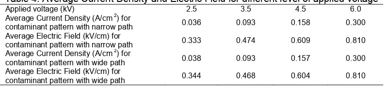
As mentioned earlier, the average value of current density and electric field for both conditions increased with the increased of applied voltage. The average current density and average electric field that presented in Table 4 shows that there is not a big gap of differences. However, the standard deviation (SD) for the current density and electric field shows a different pattern. The SD for the electric field in the wider and bend path of contaminant solution shows a small different range of 0.21 to 0.36. Meanwhile, a quite large different of the SD range of 0.17 to 1.0 reported in the electric field of straight and narrow of contaminant solution. The small standard deviation value close to zero indicates the ranges of measured data are near to the mean value. Thus, the data evaluate from the bend and wide path of contaminant are more likely to be consistent and does not differ with each value. Unlike the electric field of straight and narrow of contaminant solution, the range of measured data are in a wide range and not uniformly as at some point the value are much more large or smaller than the mean value. The SD for current density for both contaminant solution patterns is in the range of 0.0.2 to 0.37 for straight and narrow of contaminant solution while 0.04 to 0.36 for bend and wide contaminant solution. Thus, the range value measured in the current density for both circumstances is close to the average value and not varied.
Table 4. Average Current Density and Electric Field for different level of applied voltage
Applied voltage (kV) 2.5 3.5 4.5 6.0 Average Current Density (A/cm 2) for
contaminant pattern with narrow path 0.036 0.093 0.158 0.300 Average Electric Field (kV/cm) for
contaminant pattern with narrow path 0.333 0.474 0.609 0.810 Average Current Density (A/cm 2) for
contaminant pattern with wide path 0.038 0.093 0.157 0.300 Average Electric Field (kV/cm) for
contaminant pattern with wide path 0.344 0.468 0.604 0.810
3.2. Analysis on Sample with Different Loading Nanofiller
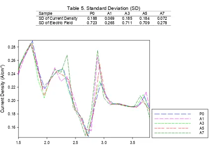
The contaminant flow rate chosen in this work is 0.6 mlmin-1with the applied voltage of 4.5 kV; this voltage level found to be most critical on material erosion [23]. Five different samples were studied by taking into consideration of dissimilar permittivity and electric conductivity as shown in Table 3. It is noticed thatthe unfilled LLDPE and natural rubber blends have the lowest permittivity and highest conductivity. Simulation analysis results show that the polymer based material without nanofiller (sample P0) recorded higher value in current density and electric field compared to other samples filled with nanofiller. The maximum value of current density and maximum electric field of LLDPE-NR blend without filler from the graph illustrated in Figure 8 had given a value of 0.289 A/cm2 and 1.111 kV/cm, respectively. Meanwhile, the samples with nanofiller have the smallest value of current density and electric field. This demonstrates that the addition of nanofiller in the blends could increase the tracking and erosion resistance. An experimental test on the same composition of sample A3 was conducted by other researchers and they found that this composition shows lowest LC and no carbon track formation. [5]. However, simulation results also show that sample A1, A3 and A5 have a good resistance in tracking and erosion test due to the lowest current density and electric field distribution of range of 0.285 to 0.286 A/cm2 and 1.09 to 1.10 kV/cm, respectively. Fig. 8 shows the current density along the insulator surface from HV electrode to the ground electrode with sample A7 shows the high average value of current density. The nanofiller more than five percent are reported as not beneficial to the blend [24]. Higher nanofiller loading in the blends tend to agglomerate in the composition. When the mixture is not uniformly dispersing, the compounds become rougher and this could lead to high LC density.
Table 5. Standard Deviation (SD)
Sample P0 A1 A3 A5 A7
SD of Current Density 0.188 0.069 0.185 0.184 0.072 SD of Electric Field 0.723 0.265 0.711 0.709 0.278
Distance from high voltage electrode to ground electrode (cm)
1.5 2.0 2.5 3.0 3.5
Current
D
ensi
ty
(A/
c
m
2 )
0.16 0.18 0.20 0.22 0.24 0.26 0.28
P0 A1 A3 A5 A7
Figure 8. Current density distribution
4. Conclusion
The model geometry of plane-parallel two dimensional has been developed in QuickField Finite Element Analysis software to study the effect of electric field distribution and current density when controlled parameters particularly applied voltage, permittivity and conductivity are varied. The simulation analysis that is conducted on the test condition of inclined plane tracking (IPT) set-up show some correlation between physical parameters involved in the IPT test condition. The physical shaped of contaminant solution path affects the current density and the electric field distribution on the insulating sample surface. Analysis on the sample with different loading of nanofiller demonstrates that sample with 1-5 % silicone oxide nanofiller gives a good resistance to tracking and erosion due to the lower value of current density and electric field obtained from simulation analysis. Thus, it can be concluded that the results obtained from simulation analysis is ingood agreement with the previous experimental results. It is believed that the results from the simulation analysis can be improved in the future by considering other factors to be included in simulation works.
Acknowledgements
The authors express their sincere gratitude to Universiti Teknologi Malaysia (UTM), for the use of facilities and by awarding a research university grants under vote03H86 and 4L133 from the Research Management Centre UTM and Malaysia Ministry of Higher Education (MOHE).
References
[1] Vasudev N, S Ganga, RS Shivakumara Aradhya, B Lalitha Pai. Effect of ATH filler content on the
performance of silicone rubber by inclined plane tracking and erosion test method. 2012 IEEE 10th
[2] Tumiran T et.al. Accelerated Aging Effect on Epoxy-polysiloxane-Rice Husk Ash Polymeric Insulator
Material. TELKOMNIKA (Telecommunication Computing Electronics and Control). 2001; 10(4) :
655-666.
[3] Venkataraman S et.al. Arc tracking resistance of polymeric materials in oxygen deficient conditions.
2003 IEE Conference in Electrical Insulation and Dielectric Phenomena. 2003: 104-107.
[4] Piah M et.al. Effect of ATH filler on the electrical tracking and erosion properties of natural
rubber-LLDPE blends under wet contaminated conditions. Journal of Industrial Technology. 2004 ; 13(1):
27-40.
[5] Jamail NAM et.al. Electrical tracking characterization of LLDPE-Natural Rubber blends filled with
nanofillers.2013 IEEE Conference in Electrical Insulation and Dielectric Phenomena (CEIDP). 2013:
695-698.
[6] Crespo-Sandova J et.al. Rate of energy absorption as indicator for the tracking/erosion test of
silicone rubber. IEEE Transactions on Dielectrics and Electrical Insulation. 2010; 17(6): 1772-1780.
[7] Vas JV, B Venkatesulu and MJ Thomas. Tracking and erosion of silicone rubber nanocomposites
under DC voltages of both polarities. IEEE Transactions on Dielectrics and Electrical Insulation.
2012; 19(1): 91-98.
[8] Kumagai S. Leakage current suppression and resistance to tracking and erosion of HTV silicone
rubber with added silicone plasticizer. IEEE Transactions on Dielectrics and Electrical Insulation.
2007; 14(2): 384-392.
[9] Rowland SM et.al. Use of image analysis in DC inclined plane tracking tests of nano and micro
composites IEEE Transactions on Dielectrics and Electrical Insulation. 2011; 18(2): 365-374.
[10] Piah MAM, A Darus, A Hassan. Electrical tracking performance of LLDPE-natural rubber blends by
employing combination of leakage current level and rate of carbon track propagation. IEEE
Transactions on Dielectrics and Electrical Insulation. 2005; 12(6): 1259-1265.
[11] Syakur A et.al. Electrical Tracking Formation on Silane Epoxy Resin under Various Contaminants.
TELKOMNIKA (Telecommunication Computing Electronics and Control). 2013; 11(1): 17-28.
[12] Syakur A et.al. Leakage current measurement of epoxy resin compound with silicon rubber. 2011
International Conference on Electrical Engineering and Informatics (ICEEI). 2011: 1-5.
[13] Yong Z et.al., Mechanism for change in leakage current waveform on a wet silicone rubber surface-a
study using a dynamic 3-D model. IEEE Transactions on Dielectrics and Electrical Insulation. 2005;
12(3): 556-565.
[14] Da Silva E and SM Rowland. The dependency of water droplet behaviour and leakage current
pattern on electrode configuration. IEEE Conference on Electrical Insulation and Dielectric
Phenomena (CEIDP '09). 2009: 242-245.
[15] Basappa P et.al. Simulation of Electric Field distribution around water droplets on outdoor insulator
surfaces. Conference Record of the 2010 IEEE International Symposium on in Electrical Insulation
(ISEI)). 2008: 50-54.
[16] Haifeng G et.al. Effect of Hydrophobicity on Electric Field Distribution and Discharges Along Various
Wetted Hydrophobic Surfaces. IEEE Transactions on Dielectrics and Electrical Insulation. 2008;
15(2): 435-443.
[17] Sarang B, P Basappa, V Lakdawala. Effect of water droplets and water films on the electrical
performance of practical outdoor insulators. Conference Record of the 2010 IEEE International
Symposium on in Electrical Insulation (ISEI). 2010: 1-6.
[18] Haoran W et.al. Simulation study on E-field distribution and corona characteristics of composite
insulator with water droplets. IEEE Conference on Electrical Insulation and Dielectric Phenomena
(CEIDP). 2013: 422-425.
[19] Illias HA, G Chen and PL Lewin. Measurement and modelling of partial discharge behaviour in a
spherical cavity within a solid dielectric material as a function of cavity diameter. 2010 10th IEEE
International Conference on Solid Dielectrics (ICSD). 2010: 1-4.
[20] Du B et.al. Dynamic behavior of water droplet for evaluating outdoor insulator.IEEE 9th International
Conference on the Properties and Applications of Dielectric Materials (ICPADM 200). 2009: 272-275.
[21] Standard B. IEC 60587 Electrical insulating materials used under severe ambient conditions-Test
methods for evaluating resistance to tracking and erosion, British Standard. 2007: 13.
[22] Jamail N et.al. Effect of Nanofillers on the Polarization and Depolarization Current Characteristics of
LLDPE-NR Compound for High Voltage Application. Advances in Material Science and Engineering.
2014: 1-7.
[23] Heger G et.al. A comparative study of insulator materials exposed to high voltage AC and DC surface
discharges. IEEE Transactions on Dielectrics and Electrical Insulation. 2010; 17(2): 513-520.
[24] Meyer LH, EA Cherney and SH Jayaram. The role of inorganic fillers in silicone rubber for outdoor

![Table 1. Test parameters [21]](https://thumb-ap.123doks.com/thumbv2/123dok/248857.504051/4.595.153.442.483.536/table-test-parameters.webp)