INVESTIGATION OF SHORT CHANNEL EFFECT ON
VERTICAL STRUCTURES IN NANOSCALE MOSFET
Munawar A. Riyadi1, Ismail Saad2, Razali Ismail3 1
Department of Electrical Engineering, Diponegoro University, Semarang 50275, Indonesia
2
School of Engineering & IT, Universiti Malaysia Sabah, 88999, Kota Kinabalu, Sabah, Malaysia
3
Faculty of Electrical Engineering, Universiti Teknologi Malaysia, 80310 Skudai, Johor, Malaysia *Corresponding author: [email protected]
Abstrak
Perkembangan MOSFET yang terkini memerlukan pendekatan inovatif untuk mempertahankan tren miniaturisasi ke dimensi nano. Makalah ini memfokuskan pada sifat fisik MOSFET vertikal dalam ukuran nano. Struktur vertikal adalah salah satu jenis devais yang menjanjikan untuk miniaturisasi lebih lanjut, dengan fitur yang tidak terikat dengan lithografi dalam pembuatannya. Perbandingan kinerja MOSFET vertikal dan lateral untuk panjang kanal Lch berukruan nano ini ditunjukkan dengan bantuan perhitungan numerik. Evaluasi parameter-parameter efek kanal pendek (short channel effect-SCE), yaitu penurunan tegangan ambang batas, subthreshold swing (SS), drain induced barrier lowering (DIBL) dan arus bocor menunjukkan keuntungan yang cukup besar, serta beberapa pertimbangan dalam menerapkan struktur tersebut, khususnya untuk ukuran nano.
Kata kunci: efek kanal pendek, MOSFET vertikal, nanoscale device, pabrikasi
Abstract
The recent development of MOSFET demands innovative approach to maintain the scaling into nanoscale dimension. This paper focuses on the physical nature of vertical MOSFET in nanoscale regime. Vertical structure is one of the promising devices in further scaling, with relaxed-lithography feature in the manufacture. The comparison of vertical and lateral MOSFET performance for nanoscale channel length (Lch) is demonstrated with the help of numerical tools. The evaluation of short channel effect (SCE) parameters, i.e. threshold voltage roll-off, subthreshold swing (SS), drain induced barrier lowering (DIBL) and leakage current shows the considerable advantages as well as its thread-off in implementing the structure, in particular for nanoscale regime.
Keywords: vertical MOSFET, devais ukuran nano, short channel effect, fabrication
1. INTRODUCTION
power, Ioff roll-off and drain induced barrier lowering (DIBL) [4]. As a result, alternative
technologies are essential as well as advanced device physics approach for overcoming these challenges.
A number of research have been conducted extensively to overcome the problem in further scaling, including the research in new materials (high-k for gate dielectric, for instance) and new device structures [5-10]. The vertical transistors have been recognized as potential solution in overcoming the scaling problems due to lithography resolution in which decananometer channels can be realized with the accuracy of ion implantation or epitaxial growth[11, 12]. A vertical MOSFET structure has its source, channel and drain arranged vertically, usually using a silicon pillar. Its channel region locates at the sidewall surface of the pillar. By this structure, the gate length definition is independent of lithography but only depends on the very well controlled vertical processing, e.g. pillar etching, thin film deposition or growth. Another possible advantage is the increased packing density as the channel width is large because of the usage of all sidewalls as channel region [13]. With the need to reduce the channel length, advancement in fabrication techniques was essential for the suppression of unwanted phenomena.
In this paper, the comparison of lateral and vertical MOSFET's performance will be presented. This paper will concentrate on single gate vertical structure compared to its lateral counterpart, different than the approach of vertically double gate transistor [14]. The solid source diffusion technique was selected in this review for its simplicity in structure and processing. In addition, its behaviour over schort channel effect will be discussed extensively by the help of numerical analysis using Silvaco technology computer-aided design (TCAD) software.
2. DEVICE STRUCTURE AND PHYSICAL MODELS
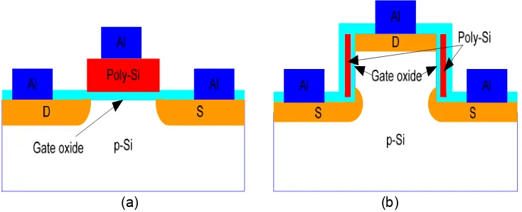
Figs. 1(a) and (b) show the basic structure of vertical and lateral MOSFET, respectively. Only one side of the vertical Si pillar is simulated, while usually both side are used, for the one-to-one comparison between the lateral and vertical structure. From this picture it is obvious that the channel is located vertically between drain and source (Fig. 1(b)), and that the definition of channel region for vertical MOSFET is lithography-independent.
(a) (b)
Fig. 1 The concept of (a) lateral and (b) vertical MOSFET
Silicon wafer with uniform boron doping of 1018 cm-3 is used as base substrate for both structures. The use of relatively high substrate doping is a consequence of device scaling which requires higher substrate doping for shorter gate length. In addition, it also gives benefit for the suppression of short channel effect [4]. A 5-nm Silicon oxide (SiO2) is grown on the substrate as
used as metal contact, and ohmic contact was assumed between metal and semiconductor. The lateral structure was designed using standard MOSFET processing sequence. In other hand, the vertical structure has additional processing steps to standard sequences, with the requirement of the trench (pillar) definition. In order to obtain clear cut pillar, isotropic etch was applied for this purpose. The height of the pillar is adjusted with the targeted channel length, and also by determining the required space for drain impurity diffusion junction.
The device structure was then simulated using SILVACO's ATLAS software package [15].Several channel lengths were simulated to understand the performance and characteristic of the devices. For the purpose of comparison study based on identical models for both devices the analysis on I-V characteristics and secondary effects are to be captured well. The Lombardi model [16] was applied as it has taken into account the mobility degradation occurs inside inversion layers through transverse and longitudinal field. In a low electric field, the carrier mobility is given using Matthiessen’s rule as
(1)
μAC is the surface mobility limited by scattering with acoustic phonons given by
(2)
where B=4.75x107 cm/s, C=1.74x10⁵, N is total doping concentration, E┴ transverse field and TL
is lattice temperature in Kelvin. μb is the mobility limited by scattering with optical intervalley
phonons given by
(3)
(4)
where μo = 52.2 cm 2
/(V.s), μ m=1417 cm 2
/(V.s), μ1 = 43.4 cm
2
/(V.s), Cr = 9.86x10 16
cm-3, Cs =
3.43x1020 cm-3, NA is the total density of impurities, μsr the surface roughness factor for
electrons and =5.82x1014 cm2/(V.s). The mobility degradation due to present of electric field is given by the relation
(5)
where μn0is the electrons low-electric-field mobility and E|| is the longitudinal electric field in the
direction of current. VSATNis the saturated drift velocity calculated from temperature-dependent
model[17].
3. RESULTS AND DISCUSSION
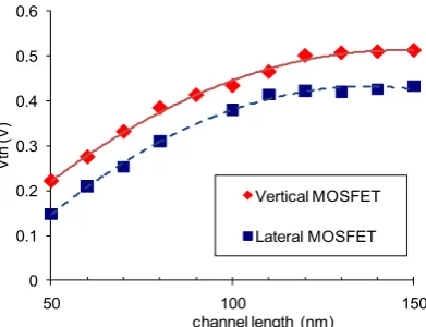
The device’s electrical properties were extracted primarily for the analysis of short channel effect. The effect of structure on the threshold voltage is shown in Figure 2. The result shows tendency of decrease in threshold voltage for decreasing channel length for both structure, while Vth decreases more dramatically below 100 nm. The threshold voltages of
vertical structure are generally higher than that of lateral, however the roll-off tendency (i.e. the rate of threshold decrease in lower channel length) for both graphs indicate that vertical structures are more likely to have better control of threshold roll-off. Worse roll-off is a sign of less control for channel, and eventually it can lead to negative threshold voltage, which requires complicated bias setup for its operation.
The value of Vth is critical for switching operation, and especially for determining the
operating region of transistor's OFF-state, which obviously lies below threshold voltage. While Vth goes higher, the corresponding off-voltage could be set more flexible, and eventually the off
current (Ioff) will be lower. But if the threshold voltage tends to be low, the off-voltage would be
forced to go lower, and tend to increase the instability of switching operation. Later, this will lead to higher Ioff, and considerably the higher power consumption at off state. However, higher Vth
could set the operating voltage at higher bias, thus it can pull the power higher in on-state. By comparing the result with recent IC manufacturing technology provided by ITRS [18], it can be seen that the threshold voltage of sub-100 nm is maintained in the order of 0.5 V. Thus, the obtained value of Vth for vertical structure (Fig. 1) is acceptable.
In the presence of high electric field i.e. Vd between source and drain, its respective
potential barrier can be affected which leads to an increased drain current, and eventually changes its threshold voltage. This parasitic effect is known as drain induced barrier lowering (DIBL), which is calculated by:
(6)
The DIBL calculation is taken for Vth at VD = 0.1 V and VD= 1.0 V, as is presented in Fig.
3. It is shown that the lateral structure has the tendency of lower DIBL for channel length above 100 nm, while the vertical offers better trend of DIBL for sub-100 nm length. This means that the vertical structure could stand for higher drain current in shorter channel with less current consumption and threshold voltage than the lateral.
0
Fig. 2 Comparison of threshold voltage (Vth)
between lateral and vertical structure
0
Fig. 3 Trend of DIBL for lateral and vertical MOSFET
(7)
where k is Boltzmann's constant, T is temperature, and Cd, Cit and Cox, are the depletion,
interface trap and oxide capacitances, respectively. The interface trap capacitance is equal to qDit., where Dit is the interface trap density. Low swing reflects a good transition time, thus lower
S value is preferable. Due to the bulk effect the sub-threshold swing of a conventional MOS transistor in bulk technology will always be higher than a certain optimum value which is roughly 60 mV/dec at room temperature.
The vertical structure gives lower subthreshold swing for overall simulated channel lengths at around 90 mV/dec. On the other hand, lateral structure has its swing rose sharply below 80 nm, although both structures have similar oxide capacitance. The depletion capacitance is considered as the influential part for the increased swing, as the lateral locate its depletion region over all junctions in the bulk, including some part of channel, whilst in vertical structure, the narrow pillar become a constraint for depletion region. In addition, the 'depth' of junction in vertical structure (see Fig.1 (b)) is essentially shallower than that of the lateral. Thus, the transition to inversion region will be faster in vertical case.
Fig. 4(b) demonstrates the leakage current of both structures. The value of Ioff was
taken for Vg = 0V and minimum drain voltage to suppress any high electric field. It can be seen
that the vertical structure have lower Ioff than that of lateral for all channel length by some order
of magnitude. The off-current increases for decreasing channel length, with the lateral structure rises more steeply in shorter channel. This confirms the phenomena of decreasing threshold voltage, as noted before. Physically, in short-channel devices the source and drain will also control of the depletion charges as well as the gate. The shared charges affected by source and drain will occupy a large fraction of total depletion charge, and later make a shift in Vth when the
gate length is decreased. While the tendency of Vth decreasing in reduced channel length is inevitable [4], the degree of reduction is the matter of concern, as it will reflects the immunity of shorter channel effect, and thus prevent the dramatically increasing power consumption, especially in off-state region.
Fig. 4 (a) Subthreshold swing (SS) of vertical and lateral MOSFET for channel length= 50-150 nm, and (b) the leakage current (Ioff) of both structures (taken at Vg=0V)
4. CONCLUSION
leakage current, by several orders of magnitude. While the subtreshold swing for both structures were found to be greater than the ideal value (i.e. 60 mV/decade), the tendency of vertical structure showed that it would give smaller variation than that of lateral for channel length below 100 nm. The value of DIBL for vertical structure is lower for channel length below 100 nm, which showed the ability to stand in higher drain current than that of lateral. As a result, the vertical structure offers better performance in shorter channel. It would also reduce power consumption and provides a good control of SCE than the lateral, especially for nanoscale devices.
REFERENCES
[1] A. Khakifirooz and D. A. Antoniadis, "MOSFET Performance Scaling--Part I: Historical Trends," IEEE Transactions on Electron Devices, vol. 55, p. 1391, 2008.
[2] P. M. Zeitzoff, "Trends and challenges in MOSFET scaling," Solid State Technology, vol. 49, pp. 42-44, Feb 2006.
[3] L. R. Harriott, "Limits of lithography," Proceedings of the IEEE, vol. 89, pp. 366-374, 2001. [4] D. J. Frank, R. H. Dennard, E. Nowak, P. M. Solomon, Y. Taur, and Hon-Sum Philip Wong,
"Device scaling limits of Si MOSFETs and their application dependencies," Proceedings of
the IEEE, vol. 89, pp. 259-288, 2001.
[5] Y. T. Hou, M. F. Li, T. Low, and D. L. Kwong, "Metal gate work function engineering on gate leakage of MOSFETs," IEEE Transactions on Electron Devices, vol. 51, pp. 1783-1789, Nov 2004.
[6] H. Wong and H. Iwai, "On the scaling issues and high-k replacement of ultrathin gate dielectrics for nanoscale MOS transistors," Microelectronic Engineering, vol. 83, pp. 1867-1904, 2006.
[7] P. Batude, X. Garros, L. Clavelier, C. Le Royer, J. M. Hartmann, V. Loup, P. Besson, L. Vandroux, Y. Campidelli, S. Deleonibus, and F. Boulanger, "Insights on fundamental mechanisms impacting Ge metal oxide semiconductor capacitors with high-k/metal gate stacks," Journal of Applied Physics, vol. 102, pp. -, Aug 1 2007.
[8] E. Gili, V. D. Kunz, C. H. de Groot, T. Uchino, P. Ashburn, D. C. Donaghy, S. Hall, Y. Wang, and P. L. F. Hemment, "Single, double and surround gate vertical MOSFETs with reduced parasitic capacitance," Solid State Electronics, vol. 48, pp. 511-519, 2004.
[9] Y. Nishi, "Scaling Limits of Silicon CMOS and Non-Silicon Opportunities," in Future Trends
in Microelectronics, S. Luryi, J. Xu, and A. Zaslavsky, Eds.: John Wiley & Sons, Inc., 2007.
[10] K. J. Kuhn, "CMOS scaling beyond 32nm: challenges and opportunities," in Proceedings of
the 46th Annual Design Automation Conference, San Francisco, California, 2009.
[11] J. Moers, "Turning the world vertical: MOSFETs with current flow perpendicular to the wafer surface," Applied Physics A: Materials Science & Processing, vol. 87, pp. 531-537, 2007.
[12] M. Masahara, Y. Liu, K. Endo, T. Matsukawa, and E. Suzuki, "Vertical Double-Gate MOSFET Device Technology," Electronics and Communications in Japan, vol. 91, pp. 46-51, 2008.
[13] T. Schulz, W. Rosner, L. Risch, A. Korbel, and U. Langmann, "Short-channel vertical sidewall MOSFETs," IEEE Transactions on Electron Devices, vol. 48, pp. 1783-1788, 2001.
[14] I. Saad and R. Ismail, "Scaling of Vertical and Lateral NMOSFET in Nanometer Regime," in
Proceedings ISESCO International Workshop and Conference on Nanotechnology, (IWCN
2007), Kuala Lumpur, 2007.
[15] Silvaco, "Product Descriptions - Virtual Wafer Fab,
http://www.silvaco.com/products/descriptions/description_vwf.html," Silvaco International, 1995.
[16] C. Lombardi, S. Manzini, A. Saporito, and M. Vanzi, "A physically based mobility model for numerical simulation ofnonplanar devices," IEEE Transactions on Computer-Aided Design
of Integrated Circuits and Systems, vol. 7, pp. 1164-1171, 1988.
[17] S. A. Schwarz and S. E. Russek, "Semi-empirical equations for electron velocity in silicon: Part I—Bulk," IEEE Transactions on Electron Devices, vol. 30, pp. 1629-1633, 1983.
[18] P. M. Zeitzoff, "2007 International Technology Roadmap: MOSFET scaling challenges,"