PROJECT COMPLETION REPORT FOR
Project Code No. : PJP2011FKEKK(39C)S00936
Report Submission Date: January 2013
Department of Computer Engineering
CHAPTER I
INTRODUCTION
Global Positioning System (GPS) is a high-precision three-dimensional real time radio
navigation system that used to determine accurate real time information. GPS system is
widely used by land, sea and airborne users anywhere in the world and in all weather
conditions. 24 hours working satellites are in orbit at 10,600 miles above the earth. They are
spaced so that from any point on earth, four satellites will be above the horizon. Each satellite
sends precise navigation messages to the ground continuously. The GPS receivers collect and
process real time information to output accurate navigation data. Due to the advantages of
global coverage, high precision and real-time positioning for all weather, GPS system is
widely used in the search and rescue, traffic management, vehicle scheduling, land, sea and air
navigation and positioning, survey and mapping all involved in the field of navigation
positioning [5].
VerilogHDL is a hardware description language that used in design, verification and
implementation of digital system in a wide range of levels of abstraction. The four levels of
abstraction included algorithmic level, register transfer level (RTL), gate level, and switch
level. The language used to control the input and output of simulation. It provides an
alternative approach to design entry by letting the designer create a text description of the
circuit without relying on a schematic. The language also defines constructs that can be used
to control the input and output of simulation [1].
This project is about real time GPS (Global Positioning System) offline tracking system which
introduces GPS system based on FPGA. GPS signal is received continuously from GPS
module and Altera FPGA board is exploited as the host for the serial data packets from the
GPS module. Verilog Hardware Description Language (VerilogHDL) is equipped with FPGA
to manipulate raw data from GPS module. Data is extracted from GPS module and proceed to
The main objective of this final year project is:
I. Implement the offline GPS tracking system based on FPGA.
II. Familiarize and use VerilogHDL to extract raw data from GPS module.
III. Manipulate the data before the program is implemented to FPGA board.
IV. Design a prototype of a smaller GPS tracking system.
1.1 Problem Statement
The commercial uses of Global Positioning System (GPS) are diverse with applications across
various industries. Some applications are simple, whereas some are complex. The growing
number of smart phones, technology convergence, mobile commerce, and location-based
shopping are all expected to boost the GPS worldwide. Due to the high demand of worldwide
market, and the feasibility of improvement to performance and applications of current
tracking system, the offline tracking system becomes the first phase of future improved online
tracking system. By exploiting FPGA board and VerilogHDL, manipulate and design the
extracted data from GPS module to build a homegrown GPS.
The complicate structure with plenty of wires and IC chips are messy to be constructed. To
construct circuit for GPS, complex circuit is needed and this causes the large size of GPS.
Hence, the problems stated may cause to spend high cost in construction, in maintenance and
in manufacturing. However by using FPGA, all these problems can be solved in easy way
which is designing GPS using Verilog HDL.
1.2 Scope of Work
By implementing Verilog HDL GPS design code to Altera DE2 board, the resulted data which
is extracted and manipulated is displayed on LCD module. Further explanation is covered in
1.3 Methodology
The project flow chart, scope of work of project, and block diagram of the project with
explanation respectively are covered in Chapter III, Methodology.
1.4 Summaries Of Chapters
This thesis is arranged into consecutively numbered chapters. Introduction explains some
important parts of whole project, objective of project, problem statement of project, scope of
work and the methodology of the project. Literature review presents the project’s details of
each single module of this project GPS tracking system. The detail explains the hardware
design of project. Research of others GPS related projects is included to show different
application of GPS. In methodology, a brief flow of project from discussing the project with
supervisor, until the end of presentation and technical report was described. Besides that, the
flow of using VerilogHDL to implement a homegrown offline GPS tracking device is shown.
Results and discussion shows the results of this project, the FPGA-based homegrown offline
GPS, assisted by VerilogHDL; and discussion on FPGA-based GPS problems faced, analysis
and simulation. Finally, results and discussion, related to objective; benefits on FPGA-based
homegrown GPS and the whole project were concluded in conclusion. The last is preparation
CHAPTER II
LITERATURE REVIEW
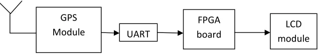
2.1Project Block Diagram
The features and modules exploited are GPS module, UART and LCD module. From Figure
2.1, GPS signal is received by antenna and goes through GPS module by UART. UART
receives data and transmits the data to FPGA board. Data from GPS (GGA, GSA, GSV, RMC,
and VTG) is filtered to get the desired data sentence while checking the validation of data
sentence at the same time. The needed data are GGA, RMC and VTG. The GPS sentence is
decoded in the physical layer and data packet is created in specific format before the data is
transferred to FPGA board. The FPGA board continuously receives the data packets from
GPS module and shows the contents of the data packets. The extracted data from GPS module
is designed by VerilogHDL and is manipulated for display on LCD module.
Figure 2.1: FPGA-Based GPS Simple Block Diagram
2.2GPS Module
GPS module is very useful for designing and developing of GPS based applications. There is
legacy port in the board to connect GPS module to FPGA board. GPS module used in this
project is GPSlim 240 Holux Wireless Bluetooth GPS Receiver. It receives signal from GPS
Module UART
FPGA board
LCD
antenna and provides variety of information. It communicates with other systems via
Bluetooth technology or USB serial communication and powered by the SIRF Star III. The
output protocol is NMEA 0183 v2.2 protocol which includes 38400 baud rate, 8 data bits, 1
stop bit and no parity used [11].
Figure 2.2: HOLUX GPSlim240
The National Marine Electronics Association (NMEA) has developed a specification that
defines the interface of various equipments [12]. This standard permits to send information.
The National Marine Electronics Association (NMEA) defined a RS232 communication
standard. GPSlim 240 communication is defined within this specification [7]. Output of
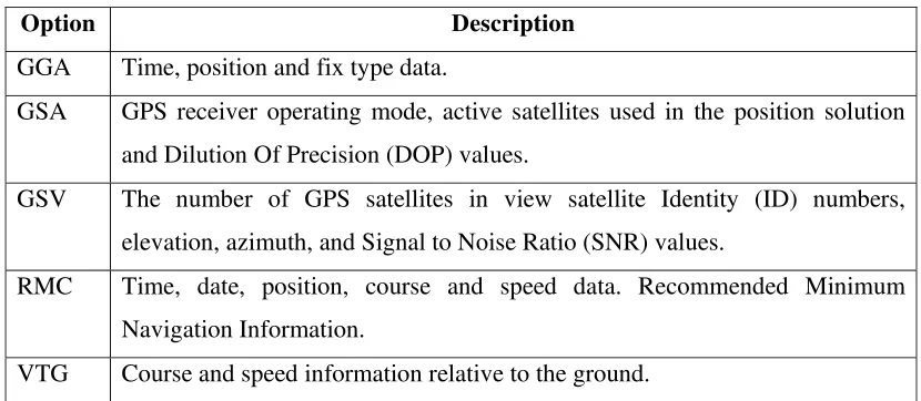
GPSlim 240 sentences are described in Table 2.1.
Table 2.1: List each of the NMEA output sentences
Option Description GGA Time, position and fix type data.
GSA GPS receiver operating mode, active satellites used in the position solution
and Dilution Of Precision (DOP) values.
GSV The number of GPS satellites in view satellite Identity (ID) numbers,
elevation, azimuth, and Signal to Noise Ratio (SNR) values.
RMC Time, date, position, course and speed data. Recommended Minimum
Navigation Information.
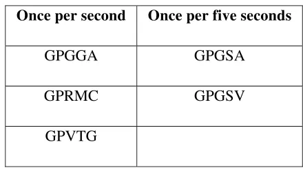
The output format of GPSlim 240 is shown in Table 2.2. GPGGA, GPRMC, GPVTG are
generated every one second. Whereas GPGSA and GPGSV produced by the GPS once per
five seconds. There are two types of data generated for every one second and every five
seconds. The first set data sequence for every second are GPGGA, GPRMC and GPVTG.
Second set data sequence are GPGGA, GPRMC, GPGSA, GPGSV, GPGSV, GPGSV, and
GPVTG.
Data headers need to be filtered and used in this project are GPGGA, GPRMC, and GPVTG.
All of these headers are produced each second. The data type detail and information will be
discussed in content 2.2.1.
Table 2.2: GPSlim 240 output format
Once per second Once per five seconds
GPGGA GPGSA
GPRMC GPGSV
GPVTG
From GPSlim 240, all data is transmitted in the form of sentences. The generated data are
ASCII characters. Each sentence starts with a "$" sign and ends with <CR><LF>. CR
(carriage return) and LF (line feed) are end of every sentence [12].
Each message starts with a dollar sign character. The next five characters identify the talker
(two characters) and the type of message (three characters). All data fields that follow are
comma-delimiter. Where data is unavailable, the corresponding field contains null bytes. The
first character that immediately follows the last data field character is an asterisk, but it is only
included if a checksum is supplied. The maximum characters in a sentence are 82 characters
[12]. In a sentence, the asterisk is immediately followed by a two-digit hexadecimal
checksum number. The checksum is the exclusive OR of all characters between the $ and *.
In this project, there are three types of GPS data need to be extracted which are GGA, RMC
2.2.1 GGA (Global Positioning System Fixed Data)
GGA is one of the GPSlim 240 output messages includes time, position and fix related data
for the GPS receiver. It is generated once per second [12].
1 2 3 4 5 6 7 8 9 10 11 12 13 14 15 | | | | | | | | | | | | | | |
$GPGGA,hhmmss.ss,llll.ll,a,yyyyy.yy,a,x,xx,x.x,x.x,M,x.x,M,x.x,xxxx*hh<CR><LF>
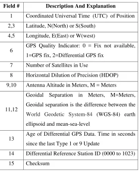
Table 2.3: GGA – GPS Fix Data Message Parameters
Field # Description And Explanation
1 Coordinated Universal Time (UTC) of Position
2,3 Latitude, N(North) or S(South)
4,5 Longitude, E(East) or W(west)
6 GPS Quality Indicator: 0 = Fix not available, 1=GPS fix, 2=Differential GPS fix
7 Number of Satellites in Use
8 Horizontal Dilution of Precision (HDOP)
9,10 Antenna Altitude in Meters, M = Meters
11,12
Geoidal Separation in Meters, M=Meters,
Geoidal separation is the difference between the
World Geodetic System-84 (WGS-84) earth
ellipsoid and mean-sea-level
13 Age of Differential GPS Data. Time in seconds since the last Type 1 or 9 Update
14 Differential Reference Station ID (0000 to 1023)
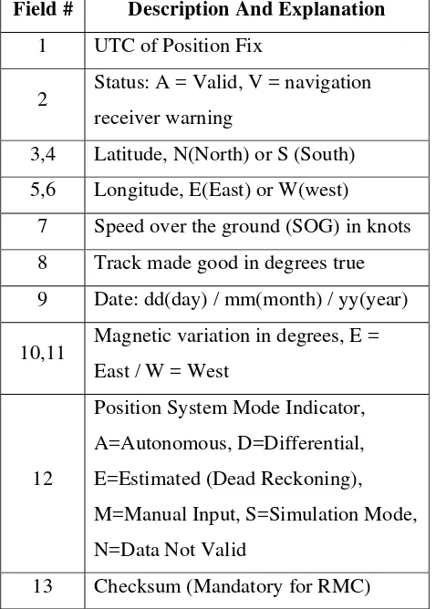
2.2.2 RMC (Recommended Minimum Specific GPS/Transit Data)
The RMC messages contain the time, date, position, course, and speed data provided by the
GPS navigation receiver [12].
1 2 3 4 5 6 7 8 9 10 111213 | | | | | | | | | | | | |
$GPRMC,hhmmss.ss,A,llll.ll,a,yyyyy.yy,a,x.x, x.x,xxxxxx,x.x,a,i*hh<CR><LF>
Table 2.4: RMC - Recommended Minimum Specific GPS/Transit Data Parameters
Field # Description And Explanation
1 UTC of Position Fix
2 Status: A = Valid, V = navigation receiver warning
3,4 Latitude, N(North) or S (South)
5,6 Longitude, E(East) or W(west)
7 Speed over the ground (SOG) in knots
8 Track made good in degrees true
9 Date: dd(day) / mm(month) / yy(year)
10,11 Magnetic variation in degrees, E = East / W = West
12
Position System Mode Indicator,
A=Autonomous, D=Differential,
E=Estimated (Dead Reckoning),
M=Manual Input, S=Simulation Mode,
N=Data Not Valid
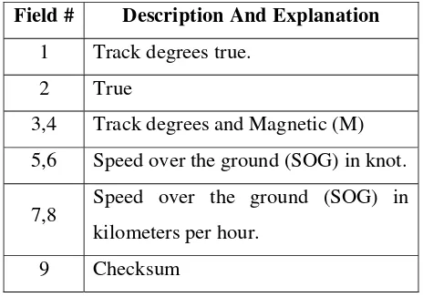
2.2.2 VTG (Course Over Ground and Ground Speed)
The VTG messages convey the actual course over ground (COG) and the speed relative to the
ground (SOG) [12].
1 2 3 4 5 6 7 8 9 | | | | | | | | |
Format: $GPVTG, x.x,T,x.x,M,x.x,N,x.x,K*hh <CR><LF>
Table 2.5: VTG – Course Over Ground and Ground Speed Parameters
Field # Description And Explanation
1 Track degrees true.
2 True
3,4 Track degrees and Magnetic (M)
5,6 Speed over the ground (SOG) in knot.
7,8 Speed over the ground (SOG) in kilometers per hour.
9 Checksum
2.3UART (Universal Asynchronous Receiver/Transmitter)
UART is commonly used in conjunction with communication standards such as EIA RS-232,
RS-422 or RS-485. Data format and transmission speeds are configurable and that the electric
signaling levels and methods are handled by a special driver circuit external to UART [1].
The UART transmits the data bits in sequential fashion by taking bytes of data. Each UART
contains a shift register which is the fundamental method of conversion between serial and
parallel forms. Serial data transmission is more effective than parallel transmission.
UART does not directly generate or receive the external signals used between different items
bits, an optional parity bit, and one or more logic high stop bits. The start bit informs the
receiver a new character is coming. The next five to eight bits represent the character of code
set employed. Next data bits may be parity bits. Following bits are always in the mark (logic
high) condition and called the stop bits. This condition presented the character is completed
[1].
Start Data 0 Data 1 Data 2 Data 3 Data 4 Data 5 Data 6 Data 7 Stop
Figure 2.3: Character Framing
UART receiver tests the state of the incoming signal on each clock pulse from start bit. If start
bit lasts one-half of the bit time, it is valid and signals the start of a new character. Else, the
spurious pulse is ignored. After waiting a further bit time, the state of the line is again sampled
and the resulting level clocked into shift register. After the required numbers of bit periods for
the character length have elapsed, the content of the shift register is made available to the
receiving system.
UART transmitter is simpler. Data is deposited in the shift register after completion of the
previous character, the UART generates a start bit, shift the required number of data bits out
to the line, generates and appends the parity bits and stop bits. The system does not proceed to
new character transmission unless the previous one is completed.
In this Project, due to the different clock frequency of GPS module and FPGA board, both of
the modules could not able to communicate to each other. UART is the connection bridge
between GPS module and FPGA board. UART receiver is taking the task of receiving the
serial bit-stream of data, and transferring the individual bit of the byte in a sequential fashion
[1]. The data arrives at a known standard bit rate but is not necessarily synchronized with the
internal clock at the host of receiver, and the transmitter’s clock is not available to the receiver.
Thus, UART generates a local clock at a higher frequency and use it to sample the received
2.4Altera Development and Education 2 (DE2) FPGA Board
Altera DE2 board is a device for design prototyping in the multimedia, storage, and
networking. It depicts the layout of the board and indicates the location of the connectors and
key components [6]. There are many features as shown in the Figure 2.4 below. It is used to
implement a wide range of designed circuits, from simple circuits to various multimedia
projects. Software support for standard Input output I/O interfaces and a control panel facility
for accessing various components are available on the board.
Figure 2.4: Altera DE2 board and Input/output (I/O) Features
VerilogHDL is used to design and manipulate the received extracted data from GPS module
on this board. For building this offline GPS, the features used in this project are: • 16x2 LCD module
• RS-232 Port
In order to use the DE2 board, familiarization with the Altera Quartus II and Modelsim
software is required. Altera Quartus II and Modelsim design software is Altera’s primary
development system. It provides a comprehensive for digital design and is an ideal platform
2.5LCD Module
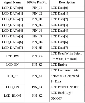
LCD module is an electronic flat panel display. Altera DE2 board LCD module has built-in
fonts and can be used to display text by sending appropriate commands to the display
controller [6]. The associated pin assignments appear in Table 2.9.
Table 2.9: Pin Assignments for the LCD Module
Signal Name FPGA Pin No. Description
LCD_DATA[0] PIN_J1 LCD Data[0]
LCD_DATA[1] PIN_J2 LCD Data[1]
LCD_DATA[2] PIN_H1 LCD Data[2]
LCD_DATA[3] PIN_H2 LCD Data[3]
LCD_DATA[4] PIN_J4 LCD Data[4]
LCD_DATA[5] PIN_J3 LCD Data[5]
LCD_DATA[6] PIN_H4 LCD Data[6]
LCD_DATA[7] PIN_H3 LCD Data[7]
LCD_RW PIN_K4 LCD Read/Write Select, 0 = Write, 1 = Read
LCD_EN PIN_K3 LCD Enable
LCD_RS PIN_K1
LCD Command/Data
Select, 0 = Command,
1= Data
LCD_ON PIN_L4 LCD Power ON/OFF
LCD_BLON PIN_K2 LCD Back Light ON/OFF
LCD module shows the information extracted from serial data packets. Time information will
be shown on LCD as hhmmss.sss. h means hour, m means minute; s means seconds. Location
will be shown as latitude, longitude, and their indicators. Apart of that, data information also
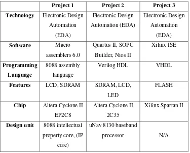
2.6 Other GPS Projects Based On FPGA
Project 1 - FPGA-Based GPS Application System Design (Pan Ming, 2009 IEEE)
The paper is about designing GPS positioning system based on FPGA and 8088 IP core. A
Cyclone II family FPGA-based navigation technology and GPS module were used to
implement the receiving terminal of the system, leads to high integration, low power
consumption, low cost, short development cycle, convenient to upgrade the product, long life
cycle, high precision, small volume, and very easy personal carry. By using EDA technology
to develop FPGA, embedding IP core of CPUs into FPGAs allows flexible communication
between user and machine because of high speed of FPGA and strong ability of a CPU in
processing information [2].
Project 2 - Real-Time GPS Receiver implemented using Altera FPGA Board (Shravani Yerabati and Zhen Hu, 2010 IEEE)
The paper presents the design challenges and implementation issues of real-time GPS receiver
based on GPS Receiver Board and Altera DE2 FPGA board. The functionalities of real time
system is to receive the data packets from GPS Receiver board continuously and to display the
time and location information using Altera DE2 board in real time mode. The designed system
also accepts set-up of desired time, so that synchronous actions can be made. These actions
will be only done once the GPS time matches the set-up time [3].
Project 3 - Design of GPS Data Acquisition and Processing System Based on FPGA (Ying Du, Jie Li, Bo Wang and Qiao Jiang, 2010)
The paper is about data acquisition and processing system based on FPGA, GPS, and FLASH.
FPGA simulates UART port, acquiring and abstracting the GPS latitude, longitude, altitude
and velocity, simultaneity, store data in real time by use of FLASH, the corresponding
experiment shows that the system can quickly and accurately transfer, acquire and store GPS
data; it is strongly suitable for various platforms of storage-type integrated measurement
2.6.1 Comparison Of Projects
Table 2.10: Comparison of Projects
Project 1 Project 2 Project 3
Features LCD, SDRAM SDRAM, LCD,
LED
FLASH
Chip Altera Cyclone II
EP2C8
Altera Cyclone II
2C35
Xilinx Spartan II
Design unit 8088 intellectual
property core, (IP
core)
uNav 8130 baseband
processor N/A
The analysis on 3 different GPS project which are FPGA-based, Project 2 is the best design. It
exploited more features from FPGA board. It is much more suitable by using Altera Quartus
II software equipped with Altera DE2 board. The project can be easily upgraded after
CHAPTER III
METHODOLOGY
3.1 Flow Chart Of Project Flow
This project started by discussing with supervisor, to identify the proposed title and objectives
of project. Next, prepare Gantt chart for guidelines and progress of project. Next, getting
understand further about the project by searching sources for related ideas and projects;
background reading and references from the similar project. Literature review is research of
the whole project in detail before project started.
After gaining enough information and research, learn and develop VerilogHDL which could
be applied on extracting data from GPS module to FPGA board. Develop the interfacing
technique for display. Next, test, analyze and diagnose the problems by using VerilogHDL
and Altera Quartus II software. The correct coding without errors is implemented to Altera
De2 board. Result on LCD screen is observed. Verify the objectives and results to be achieved
in this project. Final state of project is outcome, application, result and finalization of
Figure 3.1: Flow Chart of Project Flow Start
Discussion with supervisor
Literature review
Study of FPGA, UART functions, Verilog HDL programming, storage module and display module
Overall system testing
Finalize (Design enhancement)
End
Simulation and Synthesis of program.
Setup Altera Cyclone DE2 board
Fulfill desired result? No
Analyze and design block diagram. Convert it into Verilog HDL.
Troubleshooting and redesign
3.2 Flow Chart Of Project Work Scope
This project consists of one GPS module, UART, FPGA Altera Development and Education 2
(DE2) board and LCD screen. There are two features on Altera DE2 board are exploited
which are RS 232 port and LCD module.
First of all, analyze and design the project block diagrams and flow charts. Understand the
project flow and detail before getting start to write coding. During Verilog program codes
writing process, simulation and synthesis on the Verilog coding were also done in parallel to
troubleshoot and ensure the resultant outputs are those required.
Finally, execute the program into FPGA without errors. After the manipulated data is
extracted and transferred without errors, data is displayed on LCD module. Retest and
troubleshoot the whole program and project to get the desired result.
Figure 3.2: Flow chart of project work scope Altera Cyclone DE2 setup and implement the
program to the board. Start
Analysis and design GPS RTL, block diagrams and flow charts.
Create Verilog HDL program to describe the block diagrams and flow charts.
3.3 Block Diagram Of Project
Figure 3.3: Block diagram of Project in detail
Figure 3.3 presents the detail of the project block diagram. This project is divided into few
diagram blocks and program modules. GPS signal is received by antenna and goes through
GPS module via UART. Initialize UART and set the data length for transmit and receive as 8
bits. Transmitter of UART gets the data in unit of byte and transmits each bit of data in serial
form. At the receiver, UART re-assemble and arranges the data bits into byte before sending
to Altera DE2 board in parallel form.
When data byte is received, the flow proceeds to filter data header. Five types of data header
‘$’ sign character and end with end of line <CR><LF>. There are three out of five types are
need to be filtered to be used in this project which are GGA, RMC and VTG. Thus, headers
are filtered and used are ‘$GPGGA’, ‘$GPRMC’, and “$GPVTG’. Unused headers will be
scrapped.
Figure 3.4: Flow chart of the project program Start
UART initialization. Set baud rate to 38400.
Set the length of the reception data and receive buffer.
End
Detect and receive GPS data.
Data received?
Data processing and data header filtering.
Altera DE2 board continuously receives the data packets from GPS Module and shows the
contents of the data packets. All the data is designed by Verilog HDL. In each sentence of
data packets, the resultant checksum of exclusive OR of all characters between the $ and * is
compared to the last two ASCII characters of sentence before end of line <CR><LF>. Header
filtering and checksum comparison is done at the same time. Next, each sentence is decoded
in the physical layer. For GGA sentence, there are 14 data items. 2nd, 3rd, 4th and 5th items in
GGA sentence decoded as latitude, latitude indicator, longitude and longitude indicator. 1st
and 9th out of 12 data items in RMC sentence are decoded as time and date. Data item to be
taken from VTG sentence is only 7th out of 8 total items. It represents speed.
Data items without checksum error are stored before altering data format. Valid data items are
filtered and desired data will be displayed on Altera DE2 LCD module. Figure 3.4 shows the
flow chart of project program.
3.4 Decoding Of Data Packets
After serial data packets are received from GPS module through UART, the time information
and location information will be extracted from serial data packets, which is called decoding
of data packets [4]. Real time GPS receiver will extract the $GPGGA sentence periodically
from serial data packets. For example,
$GPGGA,211701.307,3610.5124,N,08530.4004,W,1,05,7.4,390.3,M,-30.9,M,,*6E
Extract some of the data items (UTC time, latitude and longitude) from the sentence above.
Data will be extracted as: “211701” is the time information. It indicates in hour (24 hour
format), minutes and seconds as 21 hours (9 o’clock at night), 17 minutes and 01 second.
“3610N” is the latitude information. It presents the latitude as 36 degree and 10 minutes of
North. “08530W” is the longitude information. It is 085 degree and 30 minutes of West. The
extracted position and velocity information transmit out through the FPGA simulation serials
in serial format. First, according to the baud rate of serial data processors following the
sampling clock, the sending clock was decided by the FPGA clock and the required baud rate
decision [4]. In the absence of data transmission, send ‘1’ indicating that the data line is empty,
data line at the rising edge of the sending clock, then in the next 8 consecutive clock rising
CHAPTER IV
RESULTS AND ANALYSIS
4.1 Expected Results
GPS signal received and transmitted via UART to FPGA board. GPS data is filtered and
manipulated by Verilog HDL. The desired output data are speed, date, time, latitude and
longitude. From the data, date, time, latitude and longitude are displayed on the LCD. The
displayed data on LCD module is shown as in Figure 4.1 and Table 4.1 below. LCD slots
which are circled in Figure 4.1 are from hard code of GPS program.
d d ° d d ’ N d d d ° d d ’ W
x x x . x K m / h h h : m m
Figure 4.1: GPS Information Displayed On LCD Module
Table 4.1: GPS Notes
GPS Notes Meanings
dd degrees
mm minutes
xxx.xx speed data
hh:mm hours:minutes Latitude,
North/South
Longitude,
West/East
4.2 Results and Discussion
4.2.1 Verilog HDL Module Data Sets
In this project, 3 sets of GPS data are executed. The data sets are shown as in Table 4.2. To
verify the functionality of design specifications, executing each module inputs test patterns
and analyzing the output responses. Simulation is the verification method by using testbench
as framework.
Table 4.2: GPS data sets
Set 1 Set 2 Set 3
Figure 4.2 presents the waveform of UART module. When serial data transmitted to UART
from GPS module, the ‘transmit’ signal will be triggered. After that, ‘is transmitting’ signal
and ‘is receiving’ signal will be triggered. GPS data is successfully transmitted and received
through UART from GPS module.
Figure 4.2: Waveform of UART module