Laser Anneal-Induced Effects on the NBTI Degradation of
Advanced-Process 45nm high-k PMOS
,
!
"#$#% & ' !
! ( ) ! ) ! )
Keywords: * ! + , ! - ' ! - ./ 0 1 +
Abstract. This paper presents the effects imposed on the reliability of advanced-process CMOS devices, specifically the NBTI degradation, subsequent to the integration of laser annealing (LA) in
the process flow of a 45nm HfO2/TiN gate stack PMOS device. The laser annealing temperatures
were varied from 900°C to 1350°C. The effects imposed on the NBTI degradation of the device were
comprehensively analyzed in which the shifts of the threshold voltage and drain current degradation were observed. The analysis was extended to the effects of the conventional RTA as opposed to the advanced laser annealing process. It was observed that the incorporation of laser annealing in the process flow of the device enhances the NBTI degradation rate of the device, in contrast to the integration of the conventional RTA. Laser annealing subsequent to spike-anneal is observed to improve the reliability performance of the transistor at high negative biases.
Introduction
Negative bias temperature instability (NBTI) is a reliability effect that has emerged subsequent to the rapid scaling of the CMOS technology beyond the 180nm [1] technology node. With the continued scaling of the device, along with the challenge in maintaining the device’s reliability and high performance, advanced device process integrations and enhancements are imminent. For instance, silicidation of poly [2] is introduced to reduce the polyline resistance and this in turn may result in increased silicidation consumption [3] of the source /drain diffusions. Further enhancement as raised source/drain technology [4] needed to be implemented in order to mitigate silicidation consumption. High-k dielectric with metal gate capping [5] has been introduced in submicron devices in order to continue the scaling of CMOS devices while controlling leakage current through the gate oxide. Strain engineering is being actively developed and implemented in 45nm technology node devices
[6], particularly to improve carrier mobility and saturation current, Idsat improvement. Local stress and
strain techniques are adopted and induced by techniques such as shallow trench isolation (STI) [7], strained-SiN cap layers [8] and SiGe or SiC pockets. Novel thermal processing conditions of advanced process devices had also been introduced as alternatives to the classical rapid thermal annealing (RTA). The millisecond anneal with laser [9] produces a diffusionless anneal in which it allows fast diffusion and high activation of dopants. Process enhancements such as above will improve certain characteristics of the device such as the carrier mobility, minimize short channel effect and reduce parasitic resistance of junctions.
However, the advances in the processing of the devices will in turn also affect the device reliability. Strain engineering [10] as well as high-k dielectric integration [11] had resulted in significant NBTI degradation. In this simulation study, the effects of integrating the laser annealing, the spike-anneal performed prior to the laser anneal and the conventional RTA into the process flow of an advanced-process PMOS high-k device will be comprehensively studied. This work focuses on the impact the annealing conditions imposed on the NBTI degradation of the device in which the drain current degradation and threshold voltage shifts of the device were observed and analysed. Bias
temperature stress was performed at the stress temperature of 125°C and at an applied range of negative gate biases from 0V to -1.2V.
Device Process Flow
This work studies the NBTI degradation of an advanced-process 45nm high-k PMOS device and the process flow of the studied device represents that of a generic 45nm technology node which device and manufacturing characteristics are based on the International Technology Roadmap for Semiconductor (ITRS) 2006 [12]. The process flow incorporates advanced process techniques particularly the shallow trench isolation (STI) process technique as the preferred electrical isolation scheme. Strain engineering was also introduced into the process flow in which process- stressors, specifically embedded SiGe pockets in the source and drain regions as well as dual stress liner (DSL) deposition, were incorporated to enhance the transistor’s performance. Fig.1 illustrates the process flow of the simulated 45nm high-k PMOS device [13].
Shallow Trench Isolation
Fig.1 : Process Flow of 45nm PMOS high-k device
Simulation Considerations
The high-k PMOS device is simulated using the Synopsys Sentaurus Technology CAD (TCAD) simulator tool. The tool incorporates a model which enables the laser annealing simulations in which it computes light absorption regardless of surface topography. This simulation model assumes that all absorbed light turns into heat. The simulator tool simulates heat generation and heat transport in the materials of the CMOS device in order to obtain the temperature. Below is the heat balance equation in the simulation of laser annealing adopted in this work in order to solve for the temperature of the laser-anneal [14]
device. As shown in device process flow presented in fig.1, the laser annealing is carried out subsequent to a spike-anneal which is performed at a slightly lowered temperature. Recent work [15-18] had agreed that with the implementation of the spike-anneal prior to the laser anneal, the performance of the device at higher biases are more stable. This will be further justified in the following section of this work. The laser annealing temperatures were varied in order to observe the laser induced-effects on the NBTI degradation of the device. In this simulation work, a light source of the laser anneal must be provided and such is defined by the heat fluence and heat pulse. The heat fluence in turn controls the heat generation rate, , which solves for the simulated laser anneal temperature. The laser annealing temperatures were varied by changing the laser anneal light source’s
heat fluence from a range of low to high values, and the heat temperature were solved at 1350°C,
1135°C, 1082°C and 975 °C respectively. The laser ambient temperature was at 600 °C. The
millisecond duration of the laser anneal was of 0.5ms and the spike anneal interval prior to the laser anneal was of 2s.
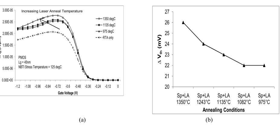
Fig. 2 : (a) Drain current degradation for different laser anneal temperatures (solid line) and for conventional rapid thermal annealing (dotted line). (b) Threshold voltage shifts for different laser anneal temperatures.
Laser anneal induces more defects at higher laser annealing temperatures as presented in fig. 2(a) and (b). The drain current degradation and the threshold voltage shifts are more significant at the
higher laser anneal temperature of 1350°C, as compared to that at a lower temperature of 975°C. The
dotted curve represents the device applied with only the conventional RTA as compared to the advanced laser-annealing process step. It is observed that the device implementing the conventional RTA produces much less current degradation and this suggests that the dopant diffusion induced by this annealing condition is different from that of the laser anneal. Millisecond annealing such as the laser anneal tends to introduce defects in the dielectric due to higher thermal stress, which resulted from high anneal temperature applied at a high annealing rate. The increasing amount of degradation as the laser anneal temperature is increased also suggests that the laser related degradation is not only due to pre-existing defects but also defects which are freshly generated. This is in agreement with an interface trap concentration study carried out by [19] in which the authors had shown that the laser-anneal temperatures influences the trap density generation of the device, which resulted in enhanced NBTI degradation. The NBTI-induced threshold voltage shifts are in the range of 20mV to 50mV, as predicted in the ITRS [20] for less than or equal to 1.2V devices. The drain voltage of the device used in this simulation is of 1.2V.
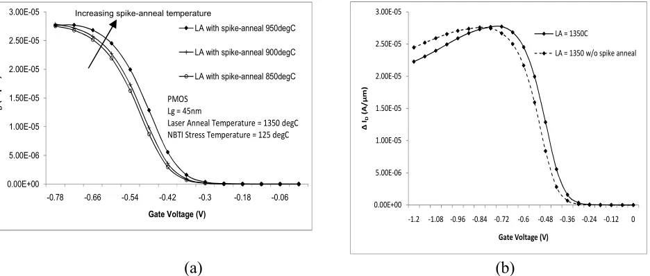
Fig.3 (a) presents the NBTI degradation of the device when the temperature of the spike-anneal is
varied at 950°C, 900°C and 850°C. It is shown that at higher spike-anneal temperatures, the NBTI
degradation is enhanced, particularly at higher negative biases. Fig. 3 (b) compares the drain current degradation of the laser-annealed (with subsequent spike-anneal) device to the device which was only annealed with the laser annealing (without subsequent spike-anneal). The figure shows that the laser-annealed device becomes less reliable at higher negative biases without the integration of the spike-anneal in the device process flow, prior to the laser-anneal process step implementation. This is due to the laser-induced defects on advanced-process devices which can be due to lattice mismatch from poor crystalline. It had also been reported [16] that the laser anneal has a lower dopant diffusion without the integration of the spike-anneal, thus resulting to less carrier mobility performance which in turn degrades the device reliability. The implementation of the spike anneal prior to laser annealing limits the creation of the laser-induced defects which results in a more stable gate dielectric and
Fig. 3 : (a) Drain current degradation for different spike anneal temperatures, prior to the implementation of laser anneal. (b) Drain current degradation for spike anneal (950°C) prior to laser anneal (solid line) compared to laser anneal only (dotted line) for laser anneal temperature of 1350°C.
Summary
This work presents the simulation of laser annealing induced-effects on the NBTI degradation of an advanced-process 45nm high-k PMOS device. The varying effects of the laser annealing temperature and spike-anneal integration were studied in terms of the NBTI-induced drain current degradation and the threshold voltage shifts. It was observed that the NBTI-induced drain current degradation and
threshold voltage shifts were significant as the laser anneal temperature was increased from 975°C to
1305°C. The spike anneal performed prior to the laser anneal effects the NBTI degradation imposed
on the advanced high-k PMOS device, though it slightly reduces the defects generated by the laser anneal. The drain current degradation is observed to increase as the spike-anneal temperature is increased.
References
[1] Pae, S. Maiz, J. Prasad, C.: IEEE International Integrated Reliability Workshop Final Report, (2007) pp 18 – 21.
[2] A.R. Saha, S. Chattopadhyay, C. Bose, C.K. Maiti : Thin Solid Films, Volume 504, Issues 1-2, 10 May 2006, Pages 86-9.
[3] Yasuhisa Omura, Kazuhisa Yoshimoto, Osanori Hayashi, Hitoshi Wakabayashi and Shinya Yamakawa : Solid-State Electronics, Volume 53, Issue 9, September 2009, Pages 959-971
[4] V. Huard, M. Denais, F. Perrier, N. Revil, C. Parthasarathy, A. Bravaix, E. Vincent : Microelectronics Reliability, Volume 45, Issue 1, January 2005, Pages 83-98.
[5] S.F. Wan Muhamad Hatta, N. Soin, D. Abd Hadiand J.F. Zhang, NBTI degradation effect on
advanced-process 45 nm high- PMOSFETs with geometric and process variations, Microelectronics Reliability, Volume 50, Issues 9-11, September-November 2010, Pages 1283-1289.
[6] 45nm High-k+Metal Gate Strain-Enhanced Transistors: Intel Technology Journal, vol 12, Issue 2, 2008.
[7] Christelle Bénard, Gaëtan Math, Pascal Fornara, Jean-Luc Ogier, Didier Goguenheim: Microelectronics Reliability, Volume 49, Issues 9-11, September-November 2009, Pages 1008-1012
[8] Tapas Kumar Maiti · Satya Sopan Mahato · Pinaki Chakraborty · Chinmay Kumar Maiti · Subir
Kumar Sarkar : J Comput Electron (2010) 9: 17
[9] A. Colin, P. Morin, R. Beneyton, Luc Pinzelli, D. Mathiot, E. Fogarassy: Thin Solid Films, Volume 518, Issue 9, 26 February 2010, Pages 2390-2393
[10] C. Claeys, E. Simoen, S. Put, G. Giusi, F. Crupi : Solid-State Electronics, Volume 52, Issue 8, August 2008, Pages 1115-1126
[11] X. Garros, M. Casse, G. Reimbold, M. Rafik, F. Martin, F. Andrieu, V. Cosnier, F. Boulanger : Microelectronic Engineering, Volume 86, Issues 7-9, July-September 2009, Pages 1609-1614.
[12] International Technology Roadmap Semiconductor (ITRS) 2006 Update, Modelling and Simulation.
[13] Sentaurus Technology Template: 45 nm reference flow and CMOS processing, (Z-2007.03). TCAD Sentaurus application note; August 2007.
[14] Sentaurus Technology Template: Simulation of Laser Annealing with Sentaurs Process, (Z-2007.03). TCAD Sentaurus application note.
[15] A. Shima, T. Mine, and K.Torii :Jpn. J. Appl. Phys. 46 (2007) pp. 1841-1847.
[16] Moonju Cho Aoulaiche, M. Degraeve, R. Ortolland, C. Kauerauf, T. Kaczer, B. Roussel, P. Hoffmann, T.Y. Groeseneken, G. : Electron Device Letters, IEEE, June 2010, pp 606 – 608
[17] C. Ortolland, L.-A.Ragnarsson, P.Favia : Symposium on VLSI Technology Digest of Technical
Papers, 2009.
[18] G. Fortunato, V. Privitera, A. La Magna, L. Mariucci, M. Cuscun et al : Thin Solid Films, Volume 504, Issues 1-2, 10 May 2006, Pages 2-6.
[19] Dong Hak Kim, Joon Won Park, You Min Chang, D. Lim, Haeyang Chung: Thin Solid Films,
Volume 518, Issue 10, 1 March 2010, Pages 2812-2815.
Laser Anneal-Induced Effects on the NBTI Degradation of Advanced-Process 45nm High-K PMOS