Electrodeposited Molybdenum Chalcogenide (MoX
2
)
Thin Films for Photovoltaic Applications
Possible alternate material for Photovotaic Applications
S. Shariza, Lim Mei Ying, T. Joseph Sahaya Anand
Department of Engineering Materials, Faculty of Manufacturing Engineering, Universiti Teknikal Malaysia Melaka,
Durian Tunggal, 76100 Melaka, Malaysia Email: [email protected]
Abstract—Thin films of molybdenum chalcogenides (MoX2, X=S,
Se and Te) have been electrosynthesized on indium-tin-oxide; (ITO)-coated glass and stainless steel substrates. The films were characterized for their structural, morphological and compositional characteristics. Their optical and semiconducting parameters were also analyzed in order to determine the suitability of the thin films for photoelectrochemical (PEC) / solar cell applications. Structural analysis via X-ray diffraction (XRD) reveals that the films are polycrystalline in nature. Scanning electron microscope (SEM) studies reveals the films were adherent to the substrate. Compositional analysis via energy dispersive X-ray (EDX) technique confirms the presence of Mo, S, Se and Te elements in the film stoichiometry. The optical studies show that the films are of direct bandgap. Results on the semiconductor parameters analysis of the films showed that the nature of the Mott-Schottky plots indicates that the films obtained are of n-type material. For all films, the semiconductor parameter value falls in the range of many other transition metal chalcogenides and this has proven that MoX2 thin films is capable
as a solar / PEC cell material
Keywords-Molybdenum chalcogenide, Thin Films, Electrodeposition, Direct bandgap, Mott-Schottky plots.
I. INTRODUCTION
Molybdenum chalcogenides (MoX2, X=S, Se and Te), one
of the many transition metal chalcogenides (TMCs) are semiconductors, which can be used as an efficient photovoltaic material. These materials have become the subject of remarkable and wide spreading technological interest [1]. The application of these materials in photoconverters, sensors as well as photoluminescent devices is becoming an important and growing area of technology [2-3]. The high production cost of solar energy materials constitutes a serious drawback for the commercialization of photovoltaic cells [4]. The economical advantages of these materials rely upon the lower level of purification needed, the low cost of synthesis and the possibility of manufacturing photovoltaic devices in thin film form, owing to their high absorption coefficients, thus allowing a considerable reduction of material consumption. For many applications, thin layers of TMC materials on substrates are normally required. The preparation of thin film materials opens the opportunity of
observing the evolution of physical properties of the materials with sizes [5]. The reduction of sizes, in terms of thickness of the thin film provide the possibility of observing novel behaviour such as size dependent structural, electrical and optical properties [6]. In this report, the electrodeposition technique at potentiostatic mode for depositing molybdenum chalcogenide thin films cathodically on ITO–coated conducting glass substrates as well as stainless steel substrates is presented. The various aspects of thin films like growth mechanism, characterization and some of its properties are discussed.
II. EXPERIMENTALDETAILS
A. Electrodeposition of molybdenum sulphide thin films The precursors molybdic acid (H2MoO4), sodium
thiosulphate pentahydrate (Na2S2O3.5H2O), selenium dioxide
(SeO2) and tellurium dioxide (TeO2) of analytical grade were
used as Mo4+, S2–, Se2– and Te2+ ion sources, respectively. ITO glass and stainless steel substrates of dimension 15 × 25 × 1 mm size were cleaned before film deposition. ITO glass were dipped into diluted hydrochloric acid, rinsed with double distilled water then cleaned in hot air while stainless steel substrates were mirror polished and finally cleaned in an ultrasonic cleaner. This treatment increases the adhesion of the electrodeposits to the substrate and allows thicker deposition without peeling.
To prepare the electrolyte solutions having relative concentrations of 0.5M H2MoO4, 0.5M SeO2, 0.5M
Na2S2O3.5H2O and 1.5mM TeO2, the following solutions were
first prepared: solution A containing H2MoO4 in ammonia,
solution B containing Na2S2O3.5H2O, solution C containing
SeO2 in distilled water and solution D containing TeO2 (99+%,
Sigma Aldrich) dissolved in sulphuric acid (95-97%, Merck). These solutions were mixed in proportional amounts as the precursor electrolyte.
For the synthesis of MoS2, MoSe2 and MoTe2, the
electrolyte mixture ratio between the precursor solutions of H2MoO4 with Na2S2O3.5H2O or SeO2 or TeO2 (where
adding drops of NaOH to the mixture. After mixing for 5 min under stirring and heating to reach a reaction temperature of 40±1 °C, the mixture is ready for synthesis of the films at 30 minutes deposition time.
The electrodeposition of the molybdenum chalcogenide, MoX2 thin films was carried out using a Princeton Applied
Research Model VersaSTAT 3 Potentiostat. The deposition potential of the molybdenum chalcogenide thin film was first derived from cyclic voltammetry (CV) technique followed by synthesis of the film by electrodeposition technique. A three – electrode cell system was adopted for the cyclic voltammetry analysis and deposition of the films. The electrolysis cell consisted of (i) an ITO-coated glass substrate or stainless steel substrate as the working electrode (WE) on which the thin film is to be deposited; (ii) graphite as the counter electrode (CE); and (iii) a saturated calomel electrode (SCE) with Ag/AgCl reference system as the reference electrode [7]. The SCE measures the potential of the working electrode. The electrode spacing should be carefully adjusted to obtain good results. Both working and counter electrodes are kept as close as 1 cm to each other and the two surfaces facing each other were kept parallel, so that released ions will be attracted and deposited exactly perpendicular to the cathode surface. The reference electrode tip is placed very close to the cathode surface so that the exact potential at the surface will be monitored unaffected by the solution resistance (internal resistance of the cell).”.
B. Characterization of Electrodeposited Thin Films
Structural and morphological film characterization for MoX2 (X=S, Se and Te) samples were determined by X-ray
diffraction (XRD) and scanning election microscopy (SEM) analysis by using PANalytical ZPERT PROMPD PW 3040/60 diffractometer (for 2θ range from 20 to 80° with CuKα radiation) and SEM ZEIZZ EVO 50 scanning microscope, respectively and its composition analysis with energy dispersive X-ray (EDX) analysis. Optical properties for determination of energy band gap of the films and semiconductor properties of the films related to its possible application in the photoelectrochemical (PEC) / solar cell were studied using UV-VIS spectrophotometer and Mott-Schottky plot analysis, respectively.
III. RESULTSANDDISCUSSION
A. Structural Characterization
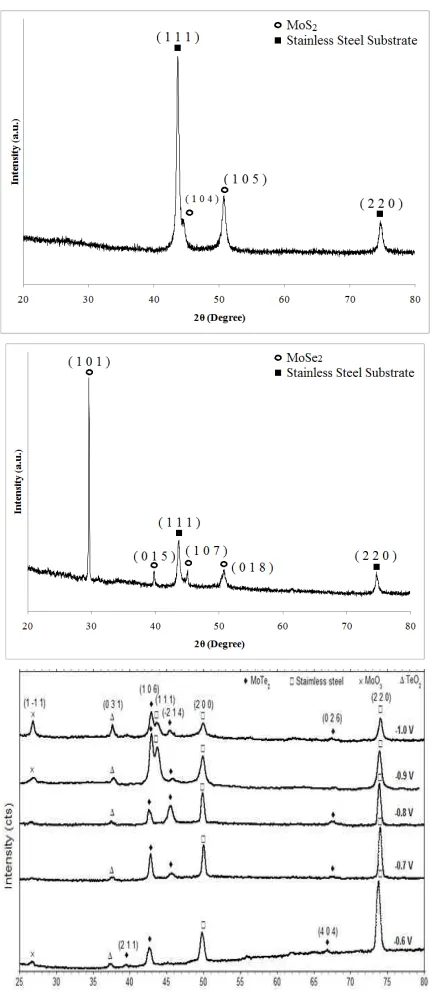
The structural characterization via XRD measurement is a diffractogram, showing phases present (peak positions), phase concentrations (peak heights), amorphous content (background hump) and crystallite size / strain (peak widths) [8]. X-ray diffraction patterns of the electrodeposited MoX2 (X=S, Se and
Te) thin films on stainless steel substrates (JCPDS Card No. 33-397) are shown in Fig. 1. The sharp peaks reveal the crystalline nature of the deposited MoX2 (X=S, Se and Te)
films. The preferred orientation is attributed to the enhancement in surface diffusion of the absorbed species resulting in crystalline peaks of MoX2 thin films. The observed
‘d’ values are compared with JCPDS standard values to determine the crystal structure.
Fig. 1. XRD diffractograms for MoS2, MoSe2 and MoTe2 thin films
The structural features fit into the hexagonal structure of the MoS2 films with lattice parameter values a = b = 0.3150
nm and c = 1.2300 nm which is in good agreement with the standard JCPDS values [9]. The diffractogram structural features fit also showed rhombohedral structure of the MoSe2
films with lattice parameter values a = b = 0.3292 nm and c = 1.9392 nm in good agreement with the standard JCPDS values [10] while MoTe2 films showed monoclinic crystal structure
According to the Debye–Scherrer approach [12], the interplanar distances‘d’ corresponding to different (h k l) planes were calculated from the X-ray diffractograms. The crystallite size was calculated from the measurement of full-width at half-maximum (FWHM) in different X-ray peaks and values are in the range of 54 – 90 nm for MoS2 films, 45 – 65
nm for MoSe2 films and 11-53 nm for MoTe2 films.
B. Morphological Characterization
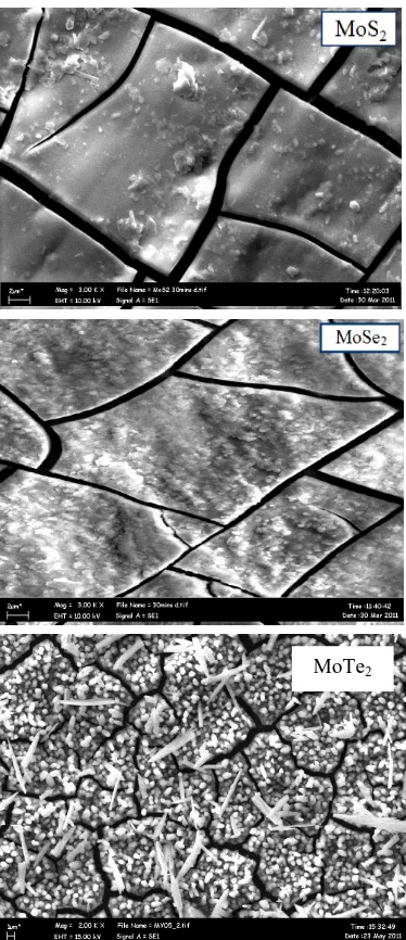
The surface morphology of MoX2 (X=S, Se and Te) thin
films deposited on stainless steel substrates is shown in Fig. 2. The structure of the films starts to crack into grains (flakes) although still adhering to the substrate. The cracking in thin films is attributed to drying shrinkage in this case of hydrous films. It has been reported that films having thickness greater than 0.2 mm are prone to cracking [13].
Fig. 2. SEM photographs for MoS2, MoSe2 and MoTe2 thin films
C. Compositional Characterization
Fig. 3 shows the EDX patterns for MoX2 (X=S, and Se)
thin films. Referring to the spectra, strong peaks for Mo, S, Se and Te were identified. It is confirmed that MoX2 (X=S and
Se) thin films have been formed through the electrodeposition process. The overlapping peaks for Mo and S elements has been identified as a limitation of the EDX technique due to the corresponding X-rays generated by emission from different energy-level shells (K, L and M). Although elements C and O do not play any role in the synthesis of the films, their peaks can be observed in the spectrum. This is due to the particular advantage of EDX whereby it possesses the capability for detection of low atomic number elements such as carbon and oxygen, which are ubiquitous in our environment. Furthermore, inclusion of oxygen is observed for all the films because it is found to be unavoidable for chemically deposited films as testified [14, 15]. This is true and accepted for all films synthesized.
Fig. 3. EDX patterns for MoS2 and MoSe2 thin films
The compositional studies of MoTe2 thin film theoretically
calculated as 33.3% and 66.7% for tellurium corresponding to its empirical formula. But the composition of the elements found by using EDX doesn’t match this stoichiometry due to presence of other elements as presented in Table 1.
Table 1: The weight percentage (wt. %) of MoTe2 with deposition potentials
-1.0 V (t = 30 minutes) and -0.9 V (t =30 minutes).
Elements (wt. %) for -1.0
V and 30 min.
(wt. %) for -0.9 V and 30 min.
Tellurium 64.84 61.89
Molybdenum 13.11 16.79
Silicon 10.83 2.94
Oxygen 9.60 13.15
Sulfur 1.62 2.34
Carbon - 2.89
The EDX analysis for MoTe2 thin film showed the
presence of other elements such as silicon, sulphide, oxygen, and carbon. The silicon is presence due to the use of ITO coated conductive glass substrate. The presence of oxygen is expected to come from the surrounding atmosphere and the oxidation of Mo / Te. The presence of sulphide and carbon are assumed as the contaminants during the experiment regarding the handling and procedures. These contaminants and other materials can be removed by annealing and the growth of thicker film.
D. Optical Properties of Electrodeposited Thin Film
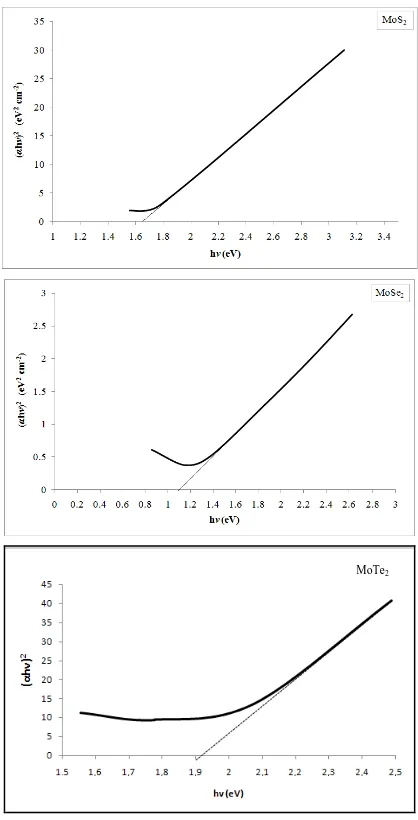
The films show good absorption in the visible region. From this absorption spectrum the band gap energy of the molybdenum disulfide thin films are calculated. From the transmittance spectrum obtained, the corresponding bandgap energy of the thin films was studied.
Fig. 4. (αhv)2 vs. hv plots of MoS2, MoSe2 and MoTe2 thin films
The optical transitions in transition metal chalcogenides films are found to be direct and allowed type [16]. Hence, a graph of (αhv)2 vs. hv is drawn and the optical bandgap energy has been estimated by extrapolating the straight line portion to cut the energy axis. Fig. 4 shows the (αhv)2 vs. hv plots of MoX2 (X=S, Se and Te) thin films. The intersection of the plots at energy axis showed bandgap energy of 1.12 eV for MoS2
films, 1.64 eV for MoSe2 films and 1.92 eV for MoTe2 films.
E. Semiconductor Parameters of Electrodeposited Thin Films A tabulation of the potential – capacitance behaviour data of MoX2 (X=S, Se and Te) thin films for the system n-MoX2 |
polyiodide| graphite electrode is done by plotting the inverse of the square of the capacitance versus the applied potential to the films. In the Mott-Schottky graphs of 1/C2 sc versus VSCE,
the voltage axis intercepts give the flat band potentials VFB.
In terms of experimental voltages, the Mott Schottky equation is defined as:
... (1)
where C is the space charge capacitance, kB is the Boltzmann’s
constant (1.38 x 10⁻²³ J/K), T is the temperature of the operation (300 K), e is the electronic charge (1.603 x 10⁻¹⁹ C), ε is the dielectric constant of the film material, εo is the
dielectric constant of free space (8.854 x 10⁻¹² F / m) and N is the carrier concentration which is calculated from the slope of the graph.
Table 2. Summary of the results obtained from the Mott–Schottky plots for MoX2 films
Semiconductor parameters MoS2 MoSe2 MoTe2
Type of semiconductor n n n
Flat band potential (VFB) (V) -0.48 -0.28 -0.61
Dielectric constant (ɛ) 27.4 33.5 23.2
Doping density (N)× 1029 (m-3) 0.48 0.72 0.37
Depletion layer width (W) (Å) 1.95 1.24 2.12
Density of states in Conduction Band (Nc)× 1013 (m-3)
4.196 4.196 4.196
Band bending (Vb) (V) 0.775 0.575 0.915
Energy gap (Eg) (eV) 1.64 1.12 1.92
Another important parameter to be deduced is the depletion layer width (W) and the band bending (Vb) that can be
calculated from the relation:
Vb = VF,redox - VFB
... (2)
MoTe2
1 2 (V – VFB – kB T / e)
C2 ɛɛ0 e N
=
where Vb is the built in voltage or the band bending and VF,redox
is the redox potential of the 2I– / I2 redox couple. An
expression for the density of states, Nc can be written as:
... (3)
where h is the Planck’s constant (4.136 x 10⁻¹⁵ eV s) me is the
effective electron mass in the conduction band and taken as ≈ 0.5 me for molybdenum chalcogenides [17]. The
semiconductor material parameters of MoX2 (X=S, Se and Te)
thin films from the Mott-Schottky plots are given in Table 2.
IV.CONCLUSION
Results proved that MoX2 (X=S, Se and Te) thin
films were successfully deposited on ITO-coated glass and stainless steel substrates. XRD analysis of the films proved polycrystalline MoX2 thin films with while EDX pattern
confirmed that mixed combinatorial films of MoX2 (X=S, Se
and Te) thin films have been formed through the electrodeposition process. Optical studies show the direct optical bandgap energy of the film in good range for a photovoltaic material. Results on the semiconductor parameters of the films revealed it is of n-type material and all semiconductor values come in the range of suitable photovoltaic material and this has proven that MoX2 (X=S, Se
and Te) thin films are capable for photoelectrochemical applications.
ACKNOWLEDGEMENT
The work described in this paper was supported by Universiti Teknikal Malaysia Melaka and Ministry of Higher Education (MoHE) sponsored FRGS grant (Project No. FRGS/2011/FKP/TK02/1 F00120).
REFERENCES
[1] A.A. Yadav, E.U. Masumdar, Photoelectrochemical performances, of n-CdS1-xSex thin films prepared by spray pyrolysis technique, Sol. Energy 84
(2010) 1445-1452.
[2] D.N. Gujarathi, G.K. Solanki, M.P. Deshpande, M.K. Agarwal, PEC behaviour of mixed single crystals of tungsten sulphoselenide grown by a CVT technique, Sol. Energy Mater. Sol. Cells 90 (2006) 2630-2639. [3] A.V. Kokate, M.R. Asabe, S.D. Delekar, L.V. Gavali, I.S. Mulla, P.P.
Hankare, B.K. Chougule, Photoelectrochemical properties of electrochemically deposited CdIn2S4 thin films, J. Phys. Chem. Solids 67
(2006) 2331-2336.
[4] A.S. Aricò, D. Silvestro, P.L. Antonucci, N. Giordano and V. Antonucci, Electrodeposited Thin Film ZnTe Semiconductors for Photovoltaic Applications, Adv. Perf. Mater. 4 (1997)115 – 125.
[5] R. S. Mane, Sankapal, B. R., Lokhande, C. D., Thickness dependent properties of chemically deposited As2S3 thin films from thioacetamide bath,
Mater.Chem. Phys. 64 (2000) 215-221.
[6] P.K. Ghosh, F. Sk. Ahmed, B. Saha, K.K. Chattopadhyay, K. K., presented at the International Workshop on Physics of Semiconductor Devices, December 16 – 20, 2007, Mumbai, India.
[7] S. Chandra, D.P. Singh, P.C. Srivastava, S.N. Sahu, Electrodeposited semiconducting molybdenum selenide films: II. Optical, electrical, electrochemical and photoelectrochemical solar cell studies, J. Phys. D: Appl. Phys. 17 (1984) 2125-2138.
[8] Fransen, M., 2002. Faster X-ray powder diffraction measurements. [9] JCPDS Data File, Card No. 2-1133
[10] JCPDS Data File, Card No. 1-72-1420 [11] JCPDS Data File, Card No. 1-71-2157
[12] Y. Chen, J. Wang, J. Lu, W. Zheng, J. Gu, S. Yang, X. Gao, Microcrystalline silicon grown by VHF PECVD and the fabrication of solar cells, Sol. Energy 82 (2008) 1083-1087.
[13] R.S. Patil, M.D. Uplane, P.S. Patil, Structural and optical properties of electrodeposited molybdenum oxide thin films, Appl. Sur. Sci. 252 (2006) 8050-8056.
[14] C.D. Lokhande, B.R. Sankapal, R.S. Mane, H.M. Pathan, M. Muller, M. Giersig, V. Ganesan, XRD, SEM, AFM, HRTEM, EDAX and RBS studies of chemically deposited Sb2S3 and Sb2Se3 thin films, Appl. Sur. Sci.193
(2002) 1-10.
[15] S. Srikanth, N. Suriyanarayanan, S. Prabahar, V. Balasubramanian, D. Kathirvel, Structural and Optical Properties of Chemical bath Deposited Sb2S3 thin films, Adv. Appl. Sci. Res. 2 (2011) 95-104.
[16] A.V. Kokate, U.B. Suryavanshi, C.H. Bhosale, Structural, compositional, and optical properties of electrochemically deposited stoichiometric CdSe thin films from non-aqueous bath, Sol. Energy 80 (2006) 156-160. [17] E. Guneri, C. Ulutas, F. Kirmizigul, G. Altindemir, F. Gode, C. Gumus,
Effect of deposition time on structural, electrical, and optical properties of SnS thin films deposited by chemical bath deposition, Appl. Sur. Sci. 257 (2010) 1189-1195.
Nc = 2 ( 2 π me* k T ) 3/2