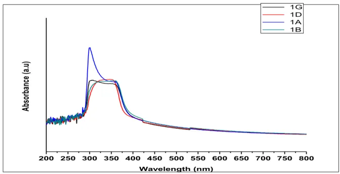
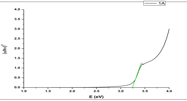
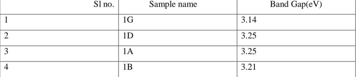
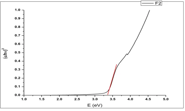
Then, this sol was used to prepare thin films of ZnO by spin coating method. The thickness of the multiple coated films was found to be around 100 nm while the roughness was measured to be around 20 nm when observed using Zeta 3D Profilometer.UV Vis. The analysis showed peaks at around 345 nm, which corresponds to the band gap of ZnO.
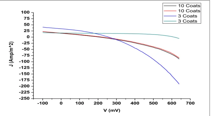
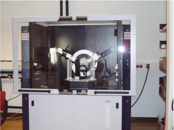
This evidence of ZnO deposition on substrates was supported by GIXRD patterns of thin films performed on a Bruker D8 Discover. XRD patterns of the samples confirmed the presence of the expected phase with few impurities. V plots showed the highest J values for cells with a film containing 3 layers of sol. Photoluminescence and absorption spectroscopy were used to observe the electron transfer process in the G1-ZnO interface.
The dye-dye (solute-solute) interaction is negligible due to the large average distance between the dye molecules. The high exciton binding energy of ZnO (~60 meV) would enable exciton transitions even at room temperature, which could mean a high radiative recombination efficiency for spontaneous emission as well as a lower threshold voltage for lasing emission. Studies have been carried out to fine-tune the properties of ZnO in order to use it for various applications; for example, the band gap of ZnO is modified for use as UV detectors and emitters.
ZnO, even though it is a II-VI semiconductor, has an ionic value which lies between that of a covalent and an ionic semiconductor.
SYNTHESIS OF MATERIALS
SYNTHESIS OF ZnO 1
SYNTHESIS of ZnO 2
UV Vis. SPECTROSCOPIC ANALYSIS
RD Measurement
Diffraction occurs due to the interaction of the waves with the repeating periodic structure of the compound in the sample. Because we have X-rays whose wavelengths are a few angstroms, which is the same as the typical interatomic distances in crystalline solids. The low intensity of diffraction from the thin top layer in the θ-2θ scan is due to the fact that the path length of the X-rays in the thin film is very short.
To improve the conditions for thin films, small angle XRD techniques such as grazing incidence X-ray diffraction (GIXRD) have been developed. As we can see, in addition to observing certain peaks that resemble the hexagonal structure of ZnO, we also get some other peaks that indicate the presence of impurities in the sample. Here we finally get some peaks mostly indicating the hexagonal structure of ZnO.
Apart from these there are some other peaks which as usual determine the existence of some other impurities in the sample.
Optical Profilometer Measurement
Dye: G1
In DSSC, the dye molecule is responsible for the optical properties of the system - it facilitates the absorption of light in the solar spectrum. A good overlap of energy levels between the lowest unoccupied molecular orbital (LUMO) of the dye and the conduction band of the semiconductor, as well as mixing of these energy levels, are important factors to initiate a fast electron transfer into the conduction band of the semiconductor. The optical properties of organic dye G1 are given by the highest occupied molecular orbital at energy 4.95 eV and lowest unoccupied molecular orbital at energy 2.74 eV.
Preparation of ZnO and Dye G1 interface
- Absorption Spectrum
The ionization potential of the electrolyte redox couple is located above the HOMO level of dye molecule to refill the hole in the dye molecule by an electron from the electrolyte. The closed-circuit current and open-circuit voltage are both dependent on energy alignment of the HOMO and LUMO dye levels. The closed circuit current of solar cell is dependent on the intensity of the incoming light and the absorption spectrum of wavelengths is limited in a DSSC in higher wavelengths.
The shape and intensity of the fluorescence spectrum is highly dependent on the nature of the sample, its concentration and the choice of solvent. At high concentration, the components of the solution (monomers, dimers, trimers, etc.) come close to each other (statistically random distribution of components), and if two neighboring components are within an interaction volume, the mutual solute interaction changes the absorption behavior. The UV Vis absorption behavior of the ZnO+G1 dye is shown in the plot below:
We can clearly see that the absorption of the dye G1 is enhanced by the presence of ZnO. Thus, the G1+ZnO interface can act as a better junction to absorb most of the emission from sunlight, as the band gap energy at the interface corresponds to a wavelength of 518 nm, which is equivalent to 2.4 eV. The photoluminescence spectra of Dye G1 and Dye G1 + ZnO are shown in the figure, obtained at an excitation wavelength of 345 nm. It shows that the peak will be at 664 nm, which is the. characteristic peak of the Dye G1 molecule.
When the dye G1 + ZnO emission spectrum was taken, the peak at 664 nm will decrease from the maximum value as shown in the figure. The photoluminescence spectra of Dye G1 and Dye G1 + ZnO are shown in the figure, obtained at an excitation wavelength of 460 nm. The peak should be at 664 nm, which is the characteristic peak of the Dye G1 molecule, but we obtained a peak at 630 nm. When the Dye G1 +ZnO emission spectrum was taken, the peak at 630 nm decreased compared to the maximum value, as shown in the figure. The open-circuit voltage is the amount of forward bias on the solar cell due to the bias of the solar cell junction with the light-generated current.
The efficiency of a solar cell is determined as the proportion of incident power that is converted into electrical energy and is defined as: Short-circuit current and open-circuit voltage are the maximum current and voltage from the solar cell, respectively. FF is defined as the ratio between the maximum power of the solar cell and the product of Voc and Isc. As for the graph, FF is a measure of the area of the largest rectangle that can fit the Ivs.V curve.
Data from Solar Cell tester
The opening voltage, VOC, is the maximum available voltage from a solar cell, and this occurs at zero current.
Preparing thin films of ZnO
Preparing Electrolyte
PREPARING Pt. ELECTRODES
TREATING THE ZnO FILMS WITH DYE
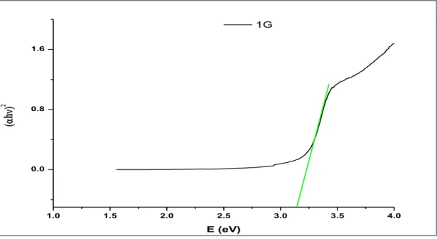
The solar cell was then prepared by depositing the FTO substrate (the side containing the film) and Pt. ZnO, being a semiconductor, has a direct band gap of 3.4 eV, which allows it to absorb the UV wavelength of sunlight. Individually, the G1 dye also has a lower absorption power, although it can absorb visible sunlight radiation.
However, when ZnO is treated with G1, the absorptivity is significantly increased than their individual selves, making the thin film ideal for absorbing the visible radiation from sunlight. Also, when tested with the cell tester (Model-CT100AAA), these DSSCs reported a maximum VOC of 612.6mV, which is considerably quite good. V-curves of these DSSCs, it may have happened that the electrolyte did not cover the thin film fully, which could have inhibited the electron injection, or it may have happened due to a defect in the substrate.