i
UNIVERSAL TIME AND CALENDAR SYSTEM IN FIELD PROGRAMMABLE GATE ARRAY (FPGA)
FATIN SHAJ BINTI AHMAD JAMAL
This Report is Submitted in Partial Fulfillment of Requirements for the Bachelor Degree of Electronic Engineering (Computer Engineering)
Fakulti Kejuruteraan Elektronik dan Kejuruteraan Komputer
Universiti Teknikal Malaysia Melaka
ii
UNIVERSTI TEKNIKAL MALAYSIA MELAKA
FAKULTI KEJURUTERAAN ELEKTRONIK DAN KEJURUTERAAN KOMPUTER
BORANG PENGESAHAN STATUS LAPORAN PROJEK SARJANA MUDA II
Tajuk Projek : Universal Time and Calendar System in FPGA.
Sesi Pengajian
:
Saya FATIN SHAJ BINTI AHMAD JAMAL.
(HURUF BESAR)
Mengaku membenarkan Laporan Projek Sarjana Muda ini disimpan di Perpustakaan dengan syarat-syarat kegunaan seperti berikut:
1. Laporan adalah hak milik Universiti Teknikal Malaysia Melaka.
2. Perpustakaan dibenarkan membuat salinan untuk tujuan pengajian sahaja.
3. Perpustakaan dibenarkan membuat salinan laporan ini sebagai bahan pertukaran antara institusi pengajian tinggi.
4. Sila tandakan ( √ ) :
SULIT*
*(Mengandungi maklumat yang berdarjah keselamatan atau kepentingan Malaysia seperti yang termaktub di dalam AKTA RAHSIA RASMI 1972)
TERHAD** **(Mengandungi maklumat terhad yang telah ditentukan oleh organisasi/badan di mana penyelidikan dijalankan)
TIDAK TERHAD
Disahkan oleh:
__________________________ ___________________________________ (TANDATANGAN PENULIS) (COP DAN TANDATANGAN PENYELIA)
iii
“Saya akui laporan ini adalah hasil kerja saya sendiri kecuali ringkasan dan petikan
yang tiap-tiap satunya telah saya jelaskan sumbernya.”
Tandatangan : ……….
NamaPenulis : ……….
iv
“Saya/kami akui bahawa saya telah membaca karya ini pada pandangan saya/kami
karya ini adalah memadai dari skop dan kualiti untuk tujuan penganugerahan Ijazah Sarjana Muda Kejuruteraan Elektronik (Kejuruteraan Komputer).”
Tandatangan : ……….
NamaPenyelia : ……….
v
vi
ACKNOWLEDGMENT
vii
ABSTRAK
viii
ABSTRACT
ix
TABLE OF CONTENTS
CHAPTER TOPIC PAGE
PROJECT TITLE i
RECOGNITION iii
DEDICATION v
ACKNOWLEDGMENT vi
ABSTRAK vii
ABSTRACT viii
LIST OF TABLES xiii
LIST OF FIGURES xiv
LIST OF SYMBOL/ABBREVIATION/TERM xvi
I INTRODUCTION 1
1.1 Project Introduction 2
1.2 Project Objectives 3
1.3 Problem Statement 3
1.4 Scope of Work 4
1.5 Methodology 4
II LITERATURE REVIEW 5
2.1 Cadence Design of Clock/Calendar
using 240*8 Bit RAM using Verilog HDL 6 2.2 FPGA Based Digital Electronic
x
TABLE OF CONTENTS
CHAPTER TOPIC PAGE
2.3 Design of Calendar Clock Based on
DS12C887 Chip 8
2.4 Design and Construction of a
Four-Hourly Digital Alarm Clock 10 2.5 Real Time Calendar Applications
in Actel Fusion Devices 11 2.6 Universal Time and Calendar System
in FPGA 12
2.7 Summary of Project Reviews 13
III METHODOLOGY 14
3.1 Flow Chart of Project 15 3.2 Block Diagram of Weekly Timer 16 3.3 Block Diagram of Universal Time
and Calendar System 18
3.4 Flow Chart of Universal Time and
Calendar Verilog Program 19
3.5 Hardware Setting 21
IV RESULTS AND DISCUSSION 23
4.1 Design Summary 24
xi
TABLE OF CONTENTS
CHAPTER TOPIC PAGE
4.2.1 Counter 60 26
4.2.2 Counter 24 27
4.2.3 Counter 7 27
4.2.4 Counter 2 29
4.2.5 Counter 12 29
4.2.6 Counter 9999 30
4.2.7 Counter 10 31
4.2.8 Counter X 31
4.2.9 Clock Division Counter 32 4.2.10 10MHz Clock Division Counter 33 4.3 Binary-Coded Decimal Module 33
4.3.1 BCD67 34
4.3.2 BCD56 34
4.3.3 BCD45 35
4.3.4 BCD14_16 36
4.4 Decimal-to-Binary Module 37 4.4.1 Dec2Bin with Booth Algorithm 38 4.5 7-Segment Display Module 39
4.6 Multiplexer Module 40
4.7 Selector Module 41
4.8 Synchronizer Module 42
4.8.1 Synchronizer 43
4.9 Top Module 44
xii
TABLE OF CONTENTS
CHAPTER TOPIC PAGE
4.10.3 Year Display 47
V CONCLUSION AND FUTURE WORK 48
5.1 Conclusion 49
5.2 Future Work 49
5.3 Business Opportunity 50
xiii
LIST OF TABLES
NUM TITLE PAGE
2.1 Summary of project reviews 13
4.1 LED Display for Days 28
xiv
LIST OF FIGURES
NUM TITLE PAGE
2.1 Block diagram of clock/calendar 6 2.2 The full counting circuit block 7 2.3 The structure of system hardware 8 2.4 The four-hourly digital alarm clock 10
2.5 Top-level block diagram 11
3.1 Flow chart of full project 15
3.2 Schematic diagram of weekly timer 17 3.3 Schematic diagram of universal time and
calendar system 18
3.4 Flow chart of universal time and calendar 20 3.5 Flow chart of hardware setting. 21
3.6 Trainer board LP-2900 22
xv
LIST OF FIGURES
NUM TITLE PAGE
4.15 Simulation waveform of BCD14_16 36 4.16 Block diagram of Dec2bin with Booth’s algorithm 37
4.17 Booth’s algorithm 38
4.18 Block diagram of 7-segment display 39 4.19 Input output block diagram of multiplexer 41 4.20 Block diagram of synchronizer circuit 43
4.21 Synchronizer simulation 43
4.22 Simulation waveform of top module block 44 4.23 Time display on 7-segment 45 4.24 Date, Month and Year display 46
xvi
LIST OF SYMBOL / ABBREVIATION / TERM
FPGA - Field Programmable Gate Array.
IC - Integrated Circuit.
PIC - Programmable Interface Controller.
HDL - Hardware Description Language.
VHDL - Very High Speed Hardware Description Language.
LED - Light Emitting Diode.
BCD - Binary-coded-decimal.
RAM - Random Access Memory.
SDA & SCL - Serial data signal in I2C bus
RTC - Real-time Clock
PC - Personal Computer
SCM - Software Configuration Management software
Iobd - Input output block diagram
Am - Ante Meridiem (before noon)
Pm - Post Meridiem (after noon)
Cntr - Counter
LUT - Look-up Table
1
CHAPTER I
INTRODUCTION
2
1.1 PROJECT INTRODUCTION
In FPGA, time and calendar system is a part of a bigger system that is implemented in our daily life such as in alarm clock, database system, registration system, punch card system and many more. This time and calendar system also known as the real time and calendar system that needs to keep the accurate time and day and has benefits such as low power consumption and more accurate than other methods. Besides, time and calendar system is often used in the form of an integrated circuit such as the PIC microcontroller. However, most of the time and calendar system were used in a discrete component that are bigger in size and expensive. This is because of the different interface use in the embedded system that used many ICs for just a simple system. Using FPGA, this problem can be solved because it does not involve any discrete component.
FPGA is also an integrated circuit that was designed for a designer to configure their design after device manufacturing. The FPGA generally used with the hardware description language to specify the configuration. Along with the Verilog Hardware Description Language (VHDL), it is the most popular and standard hardware that were used among the designers [1]. This is because Verilog offers benefits of digital hardware design with a general-purpose hardware description language same as the C programming. Thus, it is making it user friendly and easy to understand.
3
1.2 PROJECT OBJECTIVES
The aim of this project is to produce a universal time and calendar system using Field Programmable Gate Array (FPGA).
The objectives of this project are:
i. To design a Time and Calendar System in Field-Programmable Gate Array. ii. To simulate and synthesize the program using Xilinx XST.
iii. To display a Time and Calendar System through 7-segment LEDs on the LP-2900 trainerboard.
1.3 PROBLEM STATEMENT
A basic time and calendar system is usually designed by constructing a lot of gates and counters to obtain and control the functions of time and calendar. An existing basic time and calendar with a basic function such as showing time, day, month and year may need circuit constructions which consist of a few gates, BCD-to-seven-segment decoder, multiplexer, counter or some other specific ICs.These complicated structures were added more with lots of wire and ICs chip and could not be reduced due to the complex circuit.
4
1.4 SCOPE OF WORK
The scope of this project is to display a maximum of 7 days weekly timer with months and year. The time will read from zero to a maximum year = 9999, day = 6, hour = 23, minutes = 59, seconds = 59. In addition, it is also can read from one to a maximum month = 12 and day of the month = 31. The system will run by a standard quartz crystal clock 10MHz. A LP-2900 trainer board is used to test the prototype with a Xilinx FPGA chip. The FPGA is programmed using Verilog.
1.5 METHODOLOGY
5
CHAPTER II
LITERATURE REVIEW
6
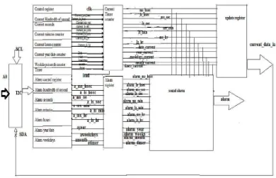
[image:22.612.145.535.99.350.2]2.1 Cadence Design of clock/calendar using 240*8 bit RAM using Verilog HDL.
Figure 2.1: Block Diagram of clock/calendar.
In this paper, it is about Cadence design clock calendar using 2048 bit RAM using Verilog HDL. This design is organized as 256 words by 8 bits with address and data are transferred serially via the two-line bidirectional I2C-bus [2]. This module is using the Verilog language with Xilinx and Cadence 90nm in Linux environment.
From the above block diagram, it consists of six modules which are counter, alarm register, sound alarm, update register, RAM and I2C. It is also included the SDA and SCL line which consist of nine clock pulse of 8 bit data. This module has a standard clock of 100 kHz.
7
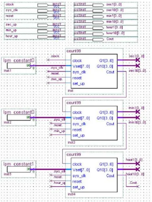
[image:23.612.224.470.96.423.2]2.2 FPGA Based Digital Electronic Education, Clock Calendar Design.
Figure 2.2: The full counting circuit block.
This paper is a case study based on the Project Based Learning for the Electronics and Computer Engineering students to design a circuit and implemented it in the FPGA. It involved with building a block from a circuit and putting the block together to get new blocks. The designed is divided into three sub block as counting, setting and display.
8
In the setting block, this is where the students will have to add something for the design according to the other blocks. This section is to help the students understand the function of the block better. It shows steps to set for the block such as using the AND gate, multiplexer, counter and decoder to be add in their design. The last task given to the student is to solve the up counting problem where it causes difficulty in usage and waste time.
The last sub block is the display block. This is the most difficult part for the student as to display the results in a flash with intervals of a second for indicating the selected unit. It used many of multiplexer in the designed thus make it more complex. This part is to analyze the results on the board and understand if the clock calendar is at normal working condition.
As for conclusion of this paper, it contains the information to study the graphic design of clock calendar system. It teaches from the basic of what circuits are involved and steps in designing a clock calendar system.This graphic design can be redesigned again using HDL codes.
[image:24.612.173.529.460.665.2]