©2012 Science Publication
doi:10.3844/ajassp.2012.1922.1928 Published Online 9 (12) 2012 (http://www.thescipub.com/ajas.toc)
Corresponding Author: Hazura Haroon, Institute of Microengineering and Nanoelectronics,Universiti Kebangsaan Malaysia,
43600 Bangi, Selangor, Malaysia
EFFECT OF LOW TEMPERATURE ON THE FABRICATION OF
MICRORING RESONATOR BY WET ETCHING
Hazura Haroon, Sahbudin Shaari, P. Susthitha Menon,
Burhanuddin Yeop Majlis, Hanim Abdul Razak and Mardiana Bidin
Institute of Microengineering and Nanoelectronics, Universiti Kebangsaan Malaysia, 43600 Bangi, Selangor, Malaysia
Received 2012-04-17, Revised 2012-10-11; Accepted 2012-11-07
ABSTRACT
Research related to semiconductor devices often relies on wafer fabrication. The fabrication of Silicon (Si) based devices by anisotropic wet etching can be affected by many etching parameters such as etching temperature, crystal orientation and percent of composition. Most of the anisotropic wet etchings by KOH solution done before were conducted at temperature over 70°C. We found that the temperatures are not suitable to fabricate ring waveguide as the waveguide wall will collapse at such high temperature. This study reports the etching characteristics of Si <100> in KOH solution with 35% concentration at the temperature below 70°C. The etched wafer is targeted to be the basic structure for Microring Resonators (MRRs) based devices. This technique provides not only lower cost as compared to other etching technique, but also simple preparation. We found that low temperature manage to mold a good ring waveguide with low tendency to form rectangular structure due to crystal orientation. At 40°C, the best waveguide formation was obtained with a smooth waveguide surface, experiencing an etching rate of 0.066 min−1 and an appreciable ring waveguide structure. The effect of the low temperature on the fabrication of the MRRs devices has been investigated and studied.
Keywords: Optical Waveguide Fabrication, Silicon Photonics, Anisotropic Chemical Etching, Microring
Resonator, Optical Filters
1. INTRODUCTION
Microring Resonators (MRRs) are of great interest for integrated optoelectronic applications due to a number of reasons; compact size, simple design and high wavelength selectivity. Its application in diverse field such as optical communications system, biochemical sensing and laser systems make it a prime selection in the design of optoelectronic devices. Among the devices that can be designed using the MRRs is filters, modulators and delay line (Hazura et al.,
2010; Shaari et al., 2010). Most of these devices can be
realized by optical waveguides where it forms the basic structure for device construction. The simplest configuration of a MRRs device consists of one straight waveguide and one circular waveguide, also known as ring resonator as shown in Fig. 1. This configuration is
commonly used in MRRs filter. The rib waveguide width for the circular waveguide, WR and the straight waveguide, WS designed in this study are 4 m and the gap distance between the straight and circular waveguides is 1 m.
Fig. 1. Schematic diagram of the MRR illustrated the
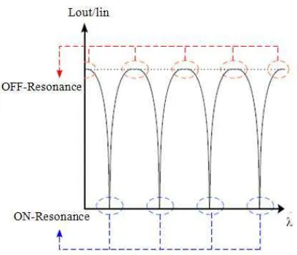
Fig. 2. Transmission spectra of MRRs filter
A typical transmission spectrum of MRRs is depicted in Fig. 2. Resonances occur when the resonant condition
as given below is satisfied (Schweb, 2004):
eff o
n L = mλ (1)
where, neff, m and λo represent the effective refractive index of the mode guided inside the ring, resonant order and resonant wavelength, respectively. L is the circumference of the ring and can be calculated by 2πR.
If Eq. 1 is not satisfied, the microring will as a condition known as OFF resonance. At OFF-resonance state, the guided wave will bypass the ring and emitted at the output port. Upon the occurrence of resonant, the guided wave in the bus waveguide will be coupled to the ring and eventually the power observed at the output port will be depleted. This condition can be explained from the simulated result obtained from commercially available software by RSoft Inc. as presented in Fig. 3.
Theoretically, power transmission at the output port or through port can be predicted by Eq. 2 (Xioa et al., 2007;
Fig. 3. Resonant condition of MRRs filter
κ2 = The power coupling coefficient between the straight waveguide and the circular waveguide κp2 = The propagation power loss coefficient per round
trip in the microring resonator
FSR is one of the key parameters of the microresonator filters, which can be calculated by Eq. 3:
observing the difference between two consecutive resonant peaks. Since we will only focus on the fabrication process, FSR will be not discussed in details in this study.
To ensure the functionality of MRRs, both two waveguide structures must be formed properly. Fabrication of these devices on single-crystal Silicon (Si) wafer can be implemented using three main methods; wet etching, dry etching and laser writing.
Depending on the applications and specifications of the proposed device, each method has its own advantages and disadvantages. Fabrication based on anisotropic wet etching was selected in our study because of low cost factor and easy preparation.
Wet etching is a process where the substrate is being immersed into etchant solutions. Typically used etchants for Si include Potassium Hydroxide (KOH), thylenediamine-pyrocatechol-water (EDP) and hydrazine-water (Seidel et al., 1990). Hydrazine water
and EDP handling must be done with special precaution because of its toxicity and instability. Despite being easily affected by several parameters such as crystals orientation, etching temperature and etchant concentration, KOH has excellent etching properties and nontoxic. For Si wafers with <100> orientation, the rib waveguide with trapezoidal cross-section angle α = 54.74°C will be formed when soaked in KOH solution.
In this study, the etching process are conducted at
discuss the characterization and the main issues arising in the Si waveguide fabrication process in the construction of MRRs device. Our focused is on the fabrication of MRR on Si using KOH wet etching at temperatures close to room temperature.
Si waveguide fabrication for MRRs device using KOH is the first in our best knowledge. The optical characterization of the device will not be discussed in this study. It should be emphasized that throughout this research, we assume that other parameters such as impurity concentration, bath condition and other contaminations are lightly influenced the fabrication performance.
2. MATERIALS AND METHODS
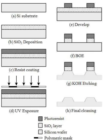
An n-type, <100>-oriented silicon wafer with 1~20Ω.cm resistivity was used as our substrates. Figure 4
illustrated the fabrication process. First, Si substrates
were cleaned using standard cleaning procedure. Approximately 1200 Å oxide layer was formed on the Si wafers using dry oxidation furnace by Carbolite after being exposed for 180 min. The temperature for the SiO2 growth was 1000°C. Through previous study (Hazura et al., 2012), the thickness is sufficient as a
mask for Si photolithography process.
Positive photoresist PR1-1000A was then spincoated on top of the oxide layer at 3000 rpm for 40 sec. This process followed by UV exposure where MRRs designs transferred onto the Si wafers. Afterwards, the Si wafer were immersed in RD6 developer from Futurex to remove unwanted resist and rinsed. The etching windows were formed by removing Silicon Dioxide (SiO2) using Buffer Oxide Etch (BOE).
The wet etching process was then carried out using 35wt % KOH aqueous solution at temperature of 33, 40, 50, 60 and 70°C without any agitation. Temperature 33°C is the minimum temperature measured when KOH solution was cooled down to room temperature. The etching process for all temperatures was performed for 15 min. Once completed, Si wafer were cleaned with deionized water to remove any residues of the process and dried using nitrogen gas.
Fig. 4. Schematic diagram showing the fabrication process
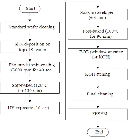
Fig. 5. Flow chart of the fabrication process
The morphological characterizations of the etched Si surfaces were then evaluated by means of Zeiss Supra Field Emission Scanning Electron Microscope (FESEM). The fabrication flow-chart of MRR is shown in Fig. 5.
3. RESULTS
Approximately 2cm2 silicon substrates were used in these experiments. The wafers were soaked in KOH solution (concentration 35%) for 15 min at 33, 40, 50, 60 and 70°C. Etch depth for the straight waveguide was measured using FESEM and the etching rate was calculated. Summary of the silicon etching rate is shown in Table 1.
Table 1 depicts the relationship of Si<100> etching
rate with KOH temperature. As the temperature increases, the etch rate is also raised.
We also compare the etch rate obtained with the other researchers works as depicted in Fig. 6 (please refer
Wilke et al., 2005; Branislav and Marija, 2010;
Kociubinski et al., 2009; Alves et al., 2005; Soin and
Majlis, 2006). It was found that the etching rate of silicon was dependable on many parameters including the bath condition, the KOH concentrations. Temperature is only one of the contributing factors affecting the etch rate. Therefore, in our study, others factors are kept constant.
Table 1. Dependence of Etching rate on KOH temperature
T (°C) Etching rate ( min−1)
33 0.037
40 0.066
50 0.181
60 0.322
70 0.531
Fig. 6. Etch rate reported before with various etching
parameters setup
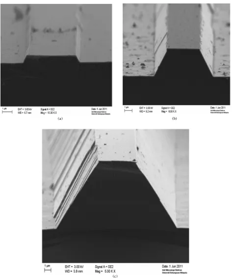
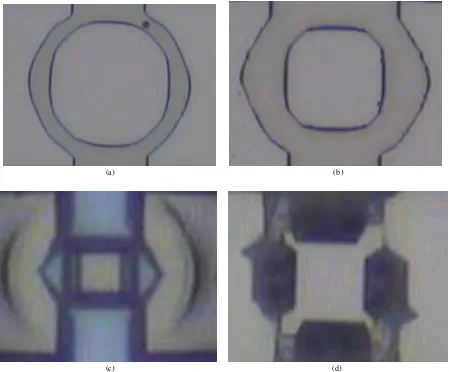
Figure 7 depict the results of the side-wall surface
roughness observed from the straight waveguide at 33°C, 50 and 70°C, respectively. It was found that an adequate surface roughness drop is observed at lower temperature. Optical microscopy pictures of Fig. 8 were taken by
observing the circular waveguide pattern from top view. It is shown that a well formed, acceptable circular waveguide structure can be mold at T = 33°C. However, the Si structure collapse gradually with an increase of etching temperature. The waveguide structure tends to shape into a rectangular at 40°C. Since KOH etching dependable on the crystal orientation, this phenomenon is understandable. At 50°C, half of the waveguide structure destroyed and the waveguide edge were totally break up at 60°C due to overetching.
4. DISCUSSION
Table 1 depicts the relationship of Si<100> etching
(a) (b)
(c)
(a) (b)
(c) (d)
Fig. 8. Microscope pictures of circular waveguides at (a) 33°C (b) 40°C (c) 50°C and (c) 60°C for 15 min etching time
Figure 6 portrays the etch rate reported before for Si
<100> with various temperatures, KOH concentrations and etching setup. Most of them were conducted at temperature over 70°C. Those results imply that the etch rate is dependable on many parameters such as etching temperature, enchants concentrations and so forth. An accurate control in handling the KOH solutions is therefore desired to sustain the exact parameter values which will directly influence the etch rate.
From Figure 7, we can see that the side-wall surface
roughens as the temperature gradually increased. The formation of so-called wavy sidewalls produced by higher temperature is expected to cause a scattering of light, which in MRRs manufacturing will resulting the reflection loss.
Figure 8 demonstrated that an acceptable etching
temperature for circular waveguide formation is ranging from 33-40°C.
5. CONCLUSION
T=40°C. The efficiency of the fabrication process will be investigated by coupling the light input into the optical waveguide in our further research.
6. ACKNOWLEDGMENT
The researcher would like to thank Universiti Teknikal Malaysia Melaka (UTeM) for the support and to the staff of Photonic Technology Lab and Clean room of Institute of Microelectronic and Nanotechnology (IMEN), Universiti Kebangsaan Malaysia for assistance and guidance. The Ministry of Higher Education of Malaysia and Universiti Kebangsaan Malaysia (UKM) is gratefully acknowledged for the grant under industrial Project-2011-015 and UKM-OUP-NBT-27-119/2011.
7. REFERENCES
Alves, M.A.R., D.F. Takeuti and E.S. Braga, 2005. Fabrication of sharp silicon tips employing anisotropic wet etching and reactive ion etching.
Micro. J., 36: 51-54. DOI:
10.1016/j.mejo.2004.10.004
Branislav, R. and R.R. Marija, 2010. Level set simulations of the anisotropic wet etching process for device fabrication in nanotechnologies. Hem.
Ind., 64: 93-97. DOI:
10.2298/HEMIND100205008R
Canavese, G., S.L. Marasso, M. Quaglio, M. Cocuzza and C. Ricciardi et al., 2007. Polymeric mask
protection for alternative KOH silicon wet etching. J. Micromech. Microeng., 17: 1387-1393. DOI: 10.1088/0960-1317/17/7/022
Hazura, H., A.R. Hanim, B. Mardiana, P.S. Menon, 2010. An analysis of silicon waveguide phase modulation efficiency based on carrier depletion effect. Proceedings of the IEEE International Conference on Semiconductor Electronics, Jun. 28-30, IEEE Xplore Press, Melaka, pp: 348-350. DOI: 10.1109/SMELEC.2010.5549519
Hazura, H., A.R. Hanim, B. Mardiana, S. Shaari and P.S. Menon, 2012. Process modeling, optimization and characterization of silicon <100> optical waveguides by anisotropic wet etching. Adv. Mater. Res. J., 403-408: 4295-4299.
Kociubinski, A., M. Duk, Bieniek and P. Janus, 2009. Modeling, simulationand calibration of silicon wet etching. J. Telecomm. Inform. Technol., 4: 65-70. Schweb, O., 2004. Transmission, group delay and
dispersion in single-ring optical resonators and add/drop filters-a tutorial overview. J. Lightwave Technol., 22: 1380-1394.
Seidel, H., L. Csepregi, A. Heuberger and H. Baumgartel, 1990. Anisotropic etching of crystalline silicon in alkaline solutions. J. Electrochem. Soc., 137: 3612-3626.DOI: 10.1149/1.2086277
Shaari, S., A.R. Hanim, B. Mardiana, H. Hazura, P.S. Menon, 2010. Modeling and analysis of lateral doping region translation variation on optical modulator performance. Proceedings of the 4th Asian Physics Symposium AIP Conference, Oct. 12-13, AIP, West Java, pp: 297-300. DOI: 10.1063/1.3537933
Soin, N. and B.Y. Majlis, 2006. Development of perfect silicon corrugated diaphragm using anisotropic etching. Microelect. Eng., 83: 1438-1441. DOI: 10.1016/j.mee.2006.01.084
Wilke, N., A. Mulcahy, S.R. Ye and A. Morrissey, 2005. Process optimization and characterization of silicon microneedles fabricated by wet etch technology.
Micro. J., 36: 650-656. DOI:
10.1016/j.mejo.2005.04.044
Xioa, S., M.H. Khan, H. Shen and M. Qi, 2007. Modeling and measurement of losses in silicon-on-insulator resonators and bends. Optics Express, 15: 10553-10561. DOI:10.1364/OE.15.010553