I hereby declare that I have read through this report entitle “A Study On Current Carrying Capacity Of Single Layer PCB” and found that has comply the partial fulfilment for awarding the degree of Bachelor of Electrical Engineering (Industrial Power).
Signature : ………..
Supervisor’s name : ………..
MUHAMMAD A'ZIM HAKIM BIN SHAHARBUDIN
A report submitted in partial fulf"illment of the requirements for the degree of Electrical Engineering (Industrial Power)
Faculty of Electrical Engineering
UNJVERSITI TEKNIKAL MALAYSIA MELAKA
ACKNOWLEDGEMENT
I would like to take this opportunity to express my gratitude to all the parties that have been assisting me throughout the duration of my final year project report.
First and foremost, I would like to shower a million thanks to my supervisor, Miss Arfah Binti Ahmad who has been of outmost help and patience. From the first I was started my final year project, until the end, she has been my source of motivation, inspiration, and my guiding light. All the input toward the meeting with her has tremendously benefited me in various aspects and kept in a corner of my mind at all times while developing this project successfully.
ABSTRACT
ABSTRAK
TABLE OF CONTENT
CHAPTER TITLE PAGE
ACKNOWLEDGEMENT I
ABSTRACT II
TABLE OF CONTENT IV
LIST OF FIGURES VI
LIST OF TABLES VII
1 INTRODUCTION 1
1.1 Background 1
1.2 Problem Statement 2
1.3 Project objective 3
1.4 Project scope 3
2 LITERATURE REVIEW 4
2.1 Introduction 5
2.2 Current Carrying Capacity 5
2.3 IPC (Interconnecting and Packaging Electronic Circuit) standard 8
2.4 Characterization of FR4 PCB 10
2.5 Thermal Design Guideline 11
2.5.1 Discussion on new design guideline 11
2.5.2 Corner effect 14 2.6 Literature review discussion 15 3 METHODOLOGY 16
3.1 Introduction 16
3.2 Methodology chart 16
3.2.1 Method 1: Find Source and Study 18
3.2.2 Method 2: Design PCB 18
4 RESULT AND ANALYSIS 23
4.1 Introduction 23
4.2 Lab testing 23
4.2.1 Straight line trace 24
4.2.2 Bended corner trace 25
4.3 Simulate Data 26
4.4 Analysis of Current, ΔT and width for straight line 28
4.4.1 Model fitting test 28
4.4.2 Straight Line before improvement 29
4.4.3 Straight line after improvement 32
4.4.4 Model Accuracy 35
4.5 Analysis of Current, ΔT and width for bended corner 37
4.5.1 Bended corner before improvement 38
4.5.2 Bended corner after improvement 41
4.5.3 Model Accuracy 44
5 CONCLUSION AND RECOMMENDATION 45
5.1 Introduction 45
5.2 Conclusion 45
5.3 Recommendation 47
REFERENCE 48
LIST OF FIGURES
FIGURE TITLE PAGE
Figure 2.1 K-Chart Map 4
Figure 2.2 Infrared thermal imaging copper conductor 7 Figure 2.3 Conductor width to cross-section relationship 8
Figure 2.4 Flaw in IPC Standard 9
Figure 2.5 A Portion of board used in IPC-TM650 12
Figure 2.6 Heat transferred in Single Layer and Double layer [6] 13 Figure 2.7 Proposed test board configuration for bended traces with round corner 14
Figure 3.1 Methodology Flow Chart 17
Figure 3.2 PCB design printed on tracing paper 19
Figure 3.3 Exposed the PCB to UV ray 19
Figure 3.4 Copper trace after etching process 20
Figure 3.5 The set-up experiment 21
Figure 3.6 Dual-Tracking DC Power Supply 22
Figure 3.7 FLIR i5 thermal imager 22
Figure 4.1 Result of 1A Single Line 24
Figure 4.2 Result of 3A Bended Corner 25
Figure 4.3 3D Graph for Straight Line 27
Figure 4.4 Regression Analysis for straight line 29
Figure 4.5 Normal probability plot of residual 31
Figure 4.6 Regression Analysis for straight line after improvement 32 Figure 4.7 Normal probability plot of residual after improvement 34
Figure 4.8 Current Estimation Graph 36
Figure 4.9 3D surface plot for bended corner 37
Figure 4.10 Minitab output for bended corner before improvement 38 Figure 4.11 Normal probability plot of bended corner before improvement 40 Figure 4.12 Minitab output for bended corner after improvement 41 Figure 4.13 Normal probability plot after improvement 43
LIST OF TABLES
TABLE TITLE PAGE
Table 2.1 Some of the common PCB material types 10 Table 2.2 Measured Temperature of Trace on PCB with M=0 and M=40mm[6] 12
1 CHAPTER 1
INTRODUCTION
1.1 Background
In recent years, the design of Printed Circuit Board (PCB) current carrying capacity such as personal computer (PC) has become increasingly dense with miniaturization of electronic packaging. At the same time, the speed of a digital electronic device used increase make more electrical current must be delivered to the device, typically via a PCB. This imposes certain limitation and critical requirement. Multi-media portable device such as hand phone and tablet phone which comes with less weight and smaller size is increasing the demand and provides an extra problem for PCB design.
Thermal management is one of the most important considerations in PCB design. The heat is distributed and dissipated during current flow which may potentially result in PCB fail to operate normally. This situation requires scheduled preventive maintenance activities as well as high operation cost. By predicting the temperature rise on the current carrying capacity of PCB, a failure on the PCB or malfunction of an electronic device can be minimized.
One of the alternative methods is by using statistical approach such as data analysis technique. This technique generally requires complete parameters to obtain a perfect solution. For problem of temperature rise on PCB which involving a complex geometries, loading and material properties, it is generally not possible to obtain a solution using this method. Beside, this method is valid for infinite number of location on the PCB. Hence, it is required to employ alternate method which is data analysis technique such as linear regression analysis.
1.2 Problem Statement
According to Institute for Interconnecting and Packaging Electronic Circuits (IPC) standard, the current carrying capacity of PCB traces represent the maximum electrical current that can be carried continuously by a trace without causing an objectionable degradation of electrical or mechanical properties of the devices. When current flowing through the copper trace and the current will generates heat in the copper will causes a deposition of thermal energy in that copper. The heat then will create a temperature rise between the trace and the surrounding environment (others microelectronic components). Hence, if the trace is exposed to a higher temperature than its limitation, the PCB could damage or worst case the PCB will explode and the electronic device will be caught on fire. This happen because the heat from the copper traces is not dissipated properly from the copper traces itself.
1.3 Project objective
There are three objectives that need to be achieved to complete this project which are 1) To study current distribution and heat dissipation of current carrying capacity. 2) To build a PCB board for data collection.
3) To develop statistical equation for modelling ideal temperature on PCB.
1.4 Project scope
This study focuses only on a single layer PCB. The base material of the board is FR4 Glass-Epoxy Single Sided. The size of the board is 150mm (width) x 300mm (length). The trace spacing of the copper is not fixed with the other copper traces. According to the journal by Mike Jouppi’s on his journal regarding current carrying capacity. Literally, there are two types of parameters that are identified to get the relationship between current and temperature rise.
2 CHAPTER 2
LITERATURE REVIEW
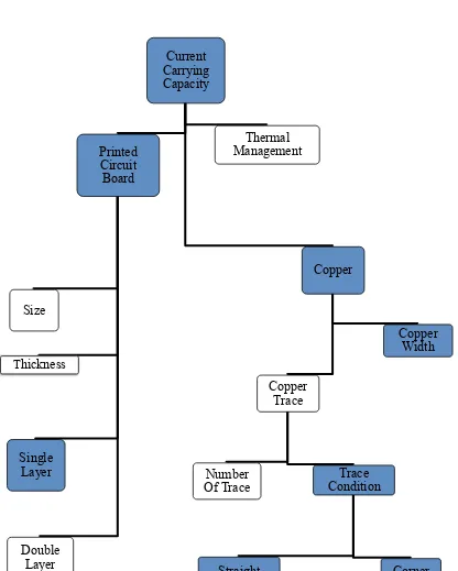
Figure 2.1 K-Chart Map Current Carrying Capacity Printed Circuit Board Single Layer Double Layer Size Thickness Copper Copper Width Copper Trace Number
Of Trace Condition Trace
Straight Corner
2.1 Introduction
This chapter highlight the past studies related to this project and background theory.
2.2 Current Carrying Capacity
Thermal management is an important design consideration in modern electronic packaging according to a journal written by Tsung-Yu Pan titled “Current Carrying of Copper Conductors in printed Wiring Boards” [1]. The author state that the requirement of the current carrying capacity of copper conductors on the surface of a printed wiring board due to temperature rise has not been studied thoroughly since the generic handbook data being published. In this journal, the author discuss more about the effect of thermal management of the copper conductors on Printed Wiring Board (PWB) or what they called now is Printed Circuit Board (PCB) having a different dimensions and arrangement. The author also stated that the experiment is used an infrared thermal as experiment basis. Then finite element analysis will be applied to correlate temperature rise versus conductor dimension and spacing, current amount and board dimensions.
Thermal resistance, Rt, has been widely used to described the thermal characteristic of electronic packaging. Rt is defined as:
(2.1)
where ΔT = temperature increase in °C, Q = heat flow rate in Watt,
To consider the heat management of copper conductor, a heat sink is not often considered because a copper conductor is usually having a big effect to PCB. So Rt is a combination of
i. Conduction through the board.
ii. Free air convection near the conductor and board surface iii. Radiation into the surrounding component.
The heat flow, Q for the copper conductor is provided by an electrical current flow through the conductor. Q is proportional to current I and resistance Re.
(2.2)
where I = current in ampere, Re = electric resistance in Ω
(2.3)
where Ρ = electric resistivity in Ω-mm, ℓ = length of the conductor in mm, t = thickness of the conductor in mm, w = width of the conductor in mm.
Figure 2.2 shows the temperature distribution on the PCB board surface across the conductor with current range of 1 to 3 ampere. It shows that thermal resistance Rt is not constant throughout the whole temperature range. This is because to the fact that Rt is a combination of conduction, free convection and radiation. Basically conduction through the board is always constant for different ambient temperature.
2.3 IPC (Interconnecting and Packaging Electronic Circuit) standard
The first standard chart that is often referred to is IPC 2152 performed by the National Bureau of Standards in 1956 [2]. According to the journal, this standard was established when printed circuit industry was in its infancy and when a guide for sizing conductor was first required. The original charts were developed from two different board materials, primarily XXXP (phenolic) and epoxy. These boards were 1/16 and 1/32 inch thick, had ½ oz, 1 oz, 2 oz and 3 oz copper conductor and some of the board had copper plane on one side of the board. The first parameters that been investigated by IPC are board material property, board thickness, copper weight and copper plane were influence trace temperature [2].
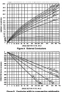
Figure 2.3 Conductor width to cross-section relationship
While working on a revision on IPC 2125, some of the journal has made criticisms about IPC 2125 regarding the design rule of PCB. The IPC Task Group 1-10b lead by Jouppi, believing the earlier version of IPC-2215 is inaccurate [3]. The close agreement between the experiment and the IPC correlation implies that the applicability of the IPC correlations is limited to PCB with little copper content. Nowadays PCB contains more copper, so that they can carry more current.
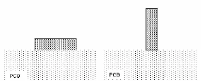
It also show that the 50% current de-rating of internal traces found in the IPC 2125 is not justified but must have been a matter of speculation at that time. Internal conductor heat and cool almost like external conductor. Another criticism is about cross sectional. Consider two traces of same cross-section, but different width w and thickness t as in figure 2.3.Let’s assume the traces have the same current, the heat spreading topology and hence cooling system will be different.
By referring to figure 2.4 the heat flow into the PCB is primarily dominated by the footprint of the traces in example the width. The horizontal trace (left) will proved better cooling than the vertical trace (right) and will carry a higher thermal power or electrical current for the same temperature rise.
2.4 Characterization of FR4 PCB
Based on the literature review, there have been few attempted studies that were conducted on characterizing certain types of FR-4 laminates and assessing the impact of lead-free soldering assembly conditions on reliability of printed circuit boards. To date, no comprehensive report is available on the effect of lead-free soldering exposures on laminate material properties. Furthermore, a wide variety of laminate types that are commercialized as ‘Lead-free process compatible’ are available recently and selection of appropriate laminates has been a challenge for the electronic industry.
An insight into the laminate material constituents and variations in their material properties due to lead-free soldering exposures is essential in the selection of appropriate laminate materials. The broad objective is to characterize a wide range of commercially available FR-4 PCB laminate materials and investigate the effects of lead-free processing on the thermo mechanical, physical, and chemical properties. The analysis is aimed at correlating the properties to the material constituents of laminates [4].
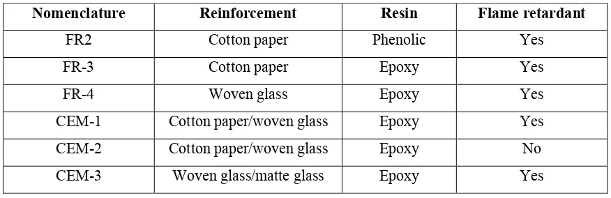
Table 2.1: Some of the common PCB material types
Nomenclature Reinforcement Resin Flame retardant
FR2 Cotton paper Phenolic Yes
FR-3 Cotton paper Epoxy Yes
FR-4 Woven glass Epoxy Yes
CEM-1 Cotton paper/woven glass Epoxy Yes
CEM-2 Cotton paper/woven glass Epoxy No
2.5 Thermal Design Guideline
A thermal design guideline which is able to reliably predict the current carrying capacity (CCC) of PCB trace will be a valuable to PCB engineer. Thus, according to YI Wang [5] in her paper describes several design guidelines for the trace CCC. YI Wang also mention some of limitation to PCB design characterized dense component and high current applied to today’s PCB. Hence, the new methods for developing a new design guidelines which are more efficient for today’s PCB design has been introduced. As mention in the second review before, many experiment and research on PCB copper trace, thermal management has been done by referring to the IPC standard and IPC has come up with IPC-2125 which is expected to be more precise and comprehensive guideline in determining PCB design. The differences between YI Wang PCB design and IPC-2125 design, which is has a flaw on designing PCB are:
1) All guidelines are based on PCB with large area space. This can hardly be found in today’s PCB
2) Single layer, multi-layers, trace corner, copper width is prevalent in PCB with more component density and high current density.
2.5.1 Discussion on new design guideline
All those guidelines gradually improved on the reliability and applicability of PCB design but none dwell on the fact that modern PCB has limited bare space. In practical, trace spacing (D) is much less than 30.5mm and sometimes less that 1mm [5].
1) To create a new standard for CCC on PCB board
2) To formulate a new PCB trace thermal design guideline which is applicable and reliable for high power density
Figure 2.5 show a different two set of PCB board with copper trace but with a different width and distance of copper trace. Figure 2.6 is exactly what is been done in this experiment which is a different width of copper trace such 0.06inch, 0.08inch and 0.10 inch but the distance between the copper trace is kept to be level of each other.
Figure 2.5
Figure 2.5: A Portion of board used in IPC-TM650
Table 2.2 is the result of investigating on the effect of trace spacing (D) with distance from edge (M) equals to 0 and 40mm. It is also show that M = 40 is appropriate to trace that are divided very widely and M = 0 appropriate to a dangerous case which the trace are hardly separated. As noticed that the trace has about 20 °C more temperature rise in case of M = 0.
Table 2.2:Measured Temperature of Trace on PCB with M=0 and M=40mm[5]