A STUDY ON CURRENT CARRYING CAPACITY OF DOUBLE LAYER PCB
MOHD AMIRUL FARUQI BIN ISMAIL BACHELOR OF ELECTRICAL ENGINEERING
“ I hereby declare that I have read through this report entitle “A Study on Current Carrying Capacity of Double Layer PCB” and found that has comply the partial fulfillment for
awarding the degree of Bachelor of Electrical Engineering (Industrial Power)”
Signature : ………..
Supervisor’s name : ………..
A STUDY ON CURRENT CARRYING CAPACITY OF DOUBLE LAYER PCB
MOHD AMIRUL FARUQI BIN ISMAIL
A report submitted in partial fulfillment of the requirements for the degree ofElectrical Engineering (Industrial Power)
Faculty of Electrical Engineering
UNIVERSITI TEKNIKAL MALAYSIA MELAKA
I declare that this report entitle “A Study on Current Carrying Capacity of Double Layer PCB” is the result of my own research except as cited in the references. The report has not been accepted for any degree and is not concurrently submitted in candidature of any other
degree.
Signature : ……….
Name : ……….
ACKNOWLEDGEMENT
Firstly, I praise to my gratitude to God for lending me a good health and patience to face all the difficulties that occurred during completed my bachelor degree final year project.
Subsequently, I would like to take this opportunity to express my sincere appreciation to my supervisor, Miss Arfah Binti Ahmad for her continuous guidance and supports, significant suggestions and critiques as well as for being an excellent supervisor. I am really appreciated very much on what she has done and a million thanks to her.
After that, I also wish to acknowledge the contributions and valuable advice provided by my lectures, who have taught me over the years in Universiti Teknikal Malaysia Melaka (UTeM). They have given me the basic principle of Electrical Engineering, and this invaluable knowledge has provided me a firm foundation for doing this project.
ABSTRACT
ABSTRAK
TABLE OF CONTENTS
CHAPTER TITLE PAGE
ACKNOWLEDGEMENT ii
ABSTRACT iii
TABLE OF CONTENTS v
LIST OF FIGURES viii
LIST OF TABLES ix
LIST OF APPENDICES x
1 INTRODUCTION 1
1.1 Background 1
1.2 Problem statement 2
1.3 Objectives 2
1.4 Scopes 3
2 LITERATURE REVIEW 4
2.1 Introduction 4
2.2 New correlations between electrical current and
temperature rise in PCB traces 5
2.2.1 FR-4 base material PCB 5
2.2.2 Traces on ceramics substrate 6 2.2.3 Trace thickness other than 35µm 7 2.3 On current carrying capacities of PCB traces 7 2.4 Thermal design guideline of PCB traces under DC
and AC current 8
2.4.1 Improvement of PCB trace thermal design
guideline 10
2.5 Current carrying capacity 12
CHAPTER TITLE PAGE
3 METHODOLOGY 15
3.1 Introduction 15
3.2 Methodology chart 15
3.2.1 Method 1: Find source and study 16
3.2.2 Method 2: Design PCB 16
3.2.3 Method 3: Experiment and data capture 17 3.2.4 Method 4: Result, analysis and discussion 19
4 RESULTS AND ANALYSIS 20
4.1 Introduction 20
4.2 Experimental results 20
4.2.1 Results captured for varied width 20
4.3 Data analysis 21
4.3.1 Analysis of temperature rise (∆T), current
(I), and width (A) for straight line 21 4.3.2 Regression analysis for straight line copper
trace 22
4.3.2.1 Regression analysis: ln (I) Vs ln
(A), ln (∆T) 23
4.3.3 Analysis of current (I), temperature rise
(∆T), and width (A) for bended corner 25 4.3.4 Regression analysis for bended corner
copper trace 27
4.3.4.1 Regression analysis: ln (I) Vs ln
(A), ln (∆T) 27
4.3.5 Analysis after transformation data for
bended corner 30
4.3.5.1 Regression analysis: ln (√I) Vs ln
(A), ln (∆T) 30
4.3.6 The regression model equation 32 4.3.6.1 Model equation for straight line
CHAPTER TITLE PAGE 4.3.6.2 Model equation for bended corner
copper trace 34
5 CONCLUSION AND RECOMMENDATION 36
5.1 Introduction 36
5.2 Conclusion 36
5.3 Recommendation 38
REFERENCES 39
LIST OF TABLES
TABLE TITLE PAGE
LIST OF FIGURES
FIGURE TITLE PAGE
2.1 K-chart for PCB characteristics 4
2.2 Mean temperature of a trace (in 20°C ambient) [3] 6 2.3 Identified current for external conductor sizing chart [2] 9 2.4 Identified cross-sectional area for external conductor sizing
chart [2]
9
2.5 Heat transfer in double-layer PCB [4] 10
2.6 Heat transfer in multi-layer PCB [4] 10
2.7 Infrared thermal picture [4] 11
3.1 Flow chart 15
3.2 Bended corner PCB 16
3.3 Straight line PCB 17
3.4 Fluke multimeter 18
3.5 FLIR thermal imager 18
3.6 DC power supply 19
4.1 Data captured for straight line 21
4.2 3-D surface plot for straight line 22
4.3 Minitab output for straight line 23
4.4 Normal probability plot of residuals 25
4.5 Data captured for bended corner 26
4.6 3-D graph for bended corner 26
4.7 Minitab output for bended corner 27
4.8 Normal probability plot for bended corner 29
4.9 Minitab output for bended corner 30
4.10 Normal probability plot for bended corner 32
4.11 Estimated current 33
4.12 Percent relative error 34
4.13 Estimated current for bender corner 35
LIST OF APPENDICES
APPENDIX TITLE PAGE
A Data captured for straight line 40
B Data captured for bended corner 41
1 CHAPTER 1
INTRODUCTION
1.1 Background
Electronic circuits manufacturing is generally manufactured through the use of PCB (Printed Circuit Board). The bare boards are made from glass reinforced plastic with copper tracks in the place of wires. Fundamentally, current carrying capacity is maximum current that can be continuously carried without causing permanent deterioration of electrical properties of a device or conductor. Damage to a PCB track may finally happen if trace is uncovered to a higher temperature than its limit. Temperature rise is basically important in making a guideline for PCB design. Current carrying capacity is the maximum quantity of electrical current a conductor or device can carry before sustaining immediate or progressive decrease. Also described as current rating or ampacity, is the root mean square (rms) electric current which a device can constantly carry while residual within its temperature rating [1].
1.2 Problem statement
Based on what has been described in previous studies, the current carrying capacity of double-layer PCB has a number of parameters that have been identified. Temperature rise on the PCB is also due to this parameter. Though, there are several parameters that do not have a significant impact of this temperature rise. Parameters can be considered as fixed values or can be ignored in this study. Consequently, to find out the critical parameters that affect the rise in temperature, the experiment is necessary.
According to the journal by L. Yun, entitled "On current carrying capacities of PCB traces," the current carrying capacity is directly comparative to square root of the trace thickness, and the roughly is directly comparative to the square root of the acceptable temperature rise [2]. When the current is higher than its rated current of PCB traces, damage may happen and operation immediately stop working. In recent years, the industries require for PCB tracks that can withstand higher power density and temperature rise has been increased. To make possible that PCB can withstand a higher power density and temperature rise, a few parameters that need to be considered such as the width, thickness, bended line, injected current or current carrying capacity, the maximum temperature of the PCB that can withstand and so on. Besides that, the temperature rise generated from power loss of copper traces. By analyzing the temperature rise on the current carrying conductor of PCB, a failure on the PCB of an electronics device can be minimized. Hence, an experiment is required to decide the parameters that influence the temperature rise on PCB.
1.3 Objectives
There are three objectives that should to be achieved to complete this project:
1. To evaluate heat distribution and dissipation of current carrying capacity of double-layer PCB.
3. To use statistical approach in analyzing data from experiment to generate model equation for double-layer PCB.
1.4 Scopes
This study only focuses on double-layer PCB. The material of double-layer PCB is FR4 as its basic material. Double-layer PCB sizes according to PCB manufacturer sold in the market that is 6 inches (width) x 11 inches (length). To discover the relationship between current and temperature rise, two parameters has been identified that are the copper width and bend angle of copper trace. For trace width used is set according to the earlier studies that are 0.06 inches, 0.08 inches, and 0.10 inches. There are two types of copper trace to be studied that are straight line and bend angle.
2 CHAPTER 2
LITERATURE REVIEW
2.1 Introduction
This chapter state about the literature review for this project. For the overall view, it is about the past study by the people or who has doing the research about the Current Carrying Capacity (CCC).
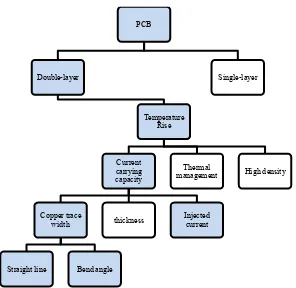
Figure 2.1 shows the K-chart for characteristics of the PCB. It consists of double-layer and single-double-layer. For this study, a double-double-layer PCBs will be more emphasized. For double-layer PCB, affecting the temperature rise is as current carrying capacity, thermal design, and high density.
Figure 2.1: K-chart for PCB characteristics
PCB Double-layer Temperature Rise Current carrying capacity Copper trace width
Straight line Bend angle
thickness Injected current Thermal
2.2 New correlations between electrical current and temperature rise in PCB traces
A correlation between electrical current and temperature rise in PCB copper traces is significant to consistently expect the current carrying capacity of a PCB according to a journal written by J. Adam [3]. This journal described about to reproduce the graphs in design rule IPC-2221 by using numerical model calculations and to evaluation it critically and to calculate current-temperature correlations. A number of parameters that influence the new correlation between electrical current and temperature rise that is:
1. FR-4 base material PCB 2. Traces on ceramics substrate 3. Trace thickness other than 35µm
2.2.1 FR-4 base material PCB
From the paper, the base material is FR-4, the copper layers PCB thickness is 1.6 mm, and trace thickness is 35 μm exceed over the PCB totally. Ambient temperature is ‘still air’ (free convection) with 20 °C. The thickness and location of added copper layers is indicated in the place in of the diagrams and is forced by typical application requirements to PCB manufacturers.
Table 2.1: Calculated current I leading to a mean temperature T [3]
Scenario Current, I(∆T=20 K)
w=2mm
Current, I (∆T=20 K)
w=10mm
1 4.0 A 12.6 A
2 5.7 A 18.7 A
3 5.5 A 17.0 A
4 7.4 A 21.0 A
5 8.4 A 23.6 A
6 7.0 A 20.6 A
7 7.2 A 22.6 A
2.2.2 Traces on ceramics substrate
Figure 2.2, shows the results for traces on a thin (0.3mm) substrate, such as a polyimide film. While this is not an accurate representation of a flex-circuit, these calculations shown that the thinner the substrate, the lower is the current-carrying capacity.
2.2.3 Trace thickness other than 35µm
The power and the track of the trace can determine the temperature for a given PCB structure. It deposits the same power and obtains the same temperature rise and provides the trace width remains the same when added double thickness and increase the current. This scaling law for trace thickness except 35 μm can be written as:
μ μ (2.1)
where, w = trace width t = trace thickness 35µ = constant
2.3 On current carrying capacities of PCB traces
In this paper, the current carrying capacity is limited due to temperature rise. For that reason, to design PCB, a few parameters that influence of temperature rise is should be identified. There are many variables that may have a significant impact on the PCB current carrying capacity. Several of those are:
i. Number of traces that are involved in current carrying ii. Trace division, or field
iii. System cooling conditions
iv. Presence or absence of the ground and/or power copper plane v. PCB size and thickness [2]
2.4 Thermal design guideline of PCB traces under DC and AC current
Founded on this journal, a thermal design guideline is very important to predict the current carrying capacity. There are previous guidelines that influences temperature rise on copper traces for example multi layers, corner effects and high frequency current their use.
The first standard chart is IPC-2221 but its main drawbacks are the sizing chart to determine PCB trace area. For sure temperature rise is fully depends on conductor cross sectional areas while other varied influences was ignored. Other drawbacks of IPC-2221 design guidelines are [4]:
i. Small copper content in the test board. The measured data acquired is conservative if applied to PCB with same size but higher copper content.
ii. Supposition that CCC of internal trace is purely 50% of an external area is oversimplified and erroneous.
iii. Trace temperature rise is separately related to cross-section area of traces and for this reason, unreliable convection effect caused by different trace faces on CCC is ignored [4].
Figure 2.3: Identified current for external conductor sizing chart [2]
Figure 2.4 shows if a trace size is identified, the temperature rise or the current can be determined. The temperature rise can be predictable only in the range among the curves of constant temperature rise. The current can be predictable if the temperature rise is given [2].
2.4.1 Improvement of PCB trace thermal design guideline
That concluded current carrying capacity results with large trace spacing, M are optimizing for the design. Improvement on current are suggested:
i. Trace spacing, M
Smaller M is a better representative for modern PCB. Corresponding results give an inherent safety margin due to presence of clearance area between traces.
Suppose that traces with current density J0 produce a loss power P on a
double-layer PCB and loss power P dissipates into ambient totally from the trace surface as shows in Figure 2.5. If traces with the same current density J in each trace in multi-layered PCB produce together the same total of loss power P, totally flowing out of the trace surface as shows in Figure 2.6, the temperature rises of the external traces in both sides must be the same. Red arrow show that heat transfer exits [4].
Figure 2.5: Heat transfer in double-layer PCB [4]
![Figure 2.2: Mean temperature of a trace (in 20°C ambient) [3]](https://thumb-ap.123doks.com/thumbv2/123dok/564992.66730/20.595.114.498.452.695/figure-mean-temperature-trace-c-ambient.webp)
![Figure 2.3: Identified current for external conductor sizing chart [2]](https://thumb-ap.123doks.com/thumbv2/123dok/564992.66730/23.595.157.455.76.297/figure-identified-current-external-conductor-sizing-chart.webp)
![Figure 2.5: Heat transfer in double-layer PCB [4]](https://thumb-ap.123doks.com/thumbv2/123dok/564992.66730/24.595.231.381.606.726/figure-heat-transfer-in-double-layer-pcb.webp)
