DEVELOPMENT OF PESONA RISC MICROPROCESSOR
ARCHITECTURE IN FPGA
MOHD FAHMIR ADZRAN BIN RAMLEE
This Report Is Submitted In Partial Fulfilment of Requirements For
The Bachelor Degree of Electronic Engineering (Computer Engineering)
Fakulti Kejuruteraan Elektronik dan Kejuruteraan Komputer
Universiti Teknikal Malaysia Melaka
“I, hereby declare that this report is the result of my own except for quotes as cited in the references.”
Signature :
Name : Mohd Fahmir Adzran Bin Ramlee
iv
“I hereby declare that I have read this report and in my opinion this report is sufficient in terms of scope and quality for the award of a Bachelor in Electronic
Engineering (Computer Engineering) with honours.”
Signature :
Name : Professor Abdul Hamid Bin Hamidon
v
Ramlee Kamal
Fatimah Mohamad Sahari
vi
vii
ABSTRACT
viii
ABSTRAK
ix
TABLE OF CONTENTS
CHAPTER TITLE PAGE
PROJECT TITLE i
REPORT AUTHORIZATION FORM ii
STUDENT’S DECLARATION iii
SUPERVISOR’S DECLARATION iv
DEDICATION v ACKNOWLEDGEMENT vi ABSTRACT vii ABSTRAK viii TABLE OF CONTENTS ix LIST OF TABLES xii TABLE OF FIGURES xiii LIST OFABBREVIATIONS xv I INTRODUCTION ... 1
1.1 Overview ... 1
1.2 Objectives... 2
1.3 Problem Statement ... 2
1.4 Scope ... 2
x
II LITERATURE REVIEW ... 4
2.1 Pesona Microprocessor ... 4
2.2 Processor in Field Programmable Gate Array (FPGA) ... 7
2.3 Harvard Architecture 11
III METHODOLOGY ... 12
3.1 Introduction ... 12
3.2 Overview ... 12
3.3 Methodology ... 13
3.4 Project Activities ... 15
3.4.1 Fetch Instruction Module ... 15
3.4.2 Decode Instruction Module ... 15
3.4.3 Execute Instruction Module ... 18
3.4.4 Module Testing ... 21
3.4.5 Behavioral Simulation ... 21
3.4.6 Debugging ... 22
3.4.7 Synthesize... 22
3.4.8 Result Analysis ... 22
3.4.9 Test Code... 22
IV RESULT AND DISCUSSION ... 24
4.1 Pesona architecture ... 24
4.2 Sources for implementation ... 26
xi
4.2.2 Control Processing Unit (CPU) Module ... 27
4.2.3 Arithmetic Logic Unit (ALU) Module ... 27
4.2.4 Instruction Decoder (IDEC) Module... 28
4.2.5 Clock Divider Module ... 28
4.2.6 Programmable Read-Only Memory (PROM) Module28 4.2.7 Dynamic Random Access Memory (DRAM) Module29 4.3 Waveform Simulation Diagram ... 30
4.4 RTL Schematic ... 33
4.5 Discussion ... 37
4.5.1 Test Code... 38
V CONCLUSION AND RECOMMENDATION 46
5.1 Conclusion ... 46
5.2 Future Recommendation ... 47
xii
LIST OF TABLES
NO. TITLE PAGES
Table 2-1 Instruction Set Summary ... 6
Table 3-1 Pesona Instruction Set ... 16
Table 3-2 Modified Pesona Instruction Sets ... 17
xiii
TABLE OF FIGURES
NO. TITLE PAGES
Figure 2-1 The 4-Stages Super-Pipeline of Pesona ... 5
Figure 2-2 MicroBlaze FPGA Board ... 8
Figure 2-3 Altera Nois II FPGA Board ... 9
Figure 2-4 Actel CoreMP7 FPGA Board ... 10
Figure 3-1 Pesona Architecture ... 13
Figure 3-2 Flow Chart of Project Methodology ... 14
Figure 3-3 Instruction Register Model ... 18
Figure 3-4 Register Programming Model ... 19
Figure 3-5 Data Space Memory Map ... 20
Figure 3-6 Sources for Behavioral Simulation ... 21
Figure 3-7 Test Code ... 23
Figure 4-1 Pesona System Diagram ... 25
Figure 4-2 Sources for implementation ... 26
Figure 4-3 PROM Module ... 29
Figure 4-4 DRAM Module ... 30
Figure 4-5 Checking on Processes ... 31
Figure 4-6 Output Waveform ... 32
Figure 4-7 Sources of simulation ... 33
Figure 4-8 Process of synthesize for RTL Schematic ... 34
Figure 4-9 Input Output Block Diagram ... 34
xiv
Figure 4-11 Component in the processor ... 36
Figure 4-12 Test Code Instruction ... 38
Figure 4-13 Test program in COE file ... 40
Figure 4-14 Instruction Set Architecture ... 41
Figure 4-15 The ‘mlo’ Operation ... 42
Figure 4-16 The ‘mhi’ Operation ... 43
Figure 4-17 The ‘add’ Operation ... 44
xv
LIST OF ABBREVIATIONS
FPGA - Field Programmable Gate Array RISC - Reduced Instruction Sets Computer ASIC - Application-Specific Integrated Circuit HDL - Hardware Description Language
SCADA - Supervisory Control and Data Acquisition ALU - Arithmetic Logic Unit
LUTs - Lookup Tables
RAM - Random Access Memory AXI - Advanced Extensible Interface MMU - Memory Management Unit FPU - Floating Point Unit
ARM - Advanced RISC Machine PC - Program Counter
RTL - Register Transfer Level P16 - Pesona 16
IC - Integrated Circuit COE - Xilinx Coefficient MUX - Multiplexer
CPU - Central Processing Unit IDEC - Instruction Decoder
DRAM - Dynamic Random Access Memory PROM - Programmable Read-Only Memory SBUS - Source Bus
DBUS - Destination Bus
xvi IR - Instruction Register
ASCII - American Standard Code for Information Interchange IP - Intellectual Property
DMIPS - Dhrystone Million Instructions per Second JTAG - Joint Test Action Group
CHAPTER I
INTRODUCTION
1.1 Overview
Pesona is a 16-bit Reduced Instruction Set Computer (RISC) Microprocessor fabricated by Mimos Semiconductor which was previously designed in Application-specific integrated circuit (ASIC) environment. Since 1996, it has never been further developed for undisclosed reason. As the first RISC processor designed by a Malaysian company, the rejuvenation of Pesona would motivate processor designer to further developed Malaysia’s own processor.
2
1.2 Objectives
The objectives of this project are as follows:
i. To emulate the original Pesona RISC architecture in Hardware Description Language.
ii.To test and verify the architecture using Xilinx Virtex-II FPGA.
1.3 Problem Statement
Since the production of Pesona in late 90’s, there were no attempts or development in upgrading or continuing the Pesona Reduced Instruction Set Computer (RISC) Microprocessor. This could be due to the lack of technological advancement in IC design technology during that particular time and also the competition from the major companies that are already established in this field. Furthermore, the prototype production cost is high and it was not economical to continue the production of this microprocessor especially during the economic recession in the late 90's.
With the emergence of the Field Programmable Gate Array (FPGA), it opens new opportunities to implement and enhance the performance of the original Pesona architecture. Specifically, Field Programmable Gate Array (FPGA) design could significantly reduce the resource utilization and also improve the clock cycle of the instruction execution time
1.4 Scope
3
1.5 Report Structure
Chapter I briefs about the objectives, scope and problem statement of this project.
Chapter II presents in detail the architecture and characteristics of the Pesona Microprocessor. The basic architecture and its origin specification were discussed. It also includes the studies on development and implementation tool in order to implement it in FPGA. Chapter II also contains information regarding the development of microprocessor in FPGA and some examples.
Chapter III gives the methodology requirement on completing the task. All necessary information is included and is supported by flow chart to summarize the method used.
Chapter IV presents the result for this project. All information regarding the results obtained was discussed.
4
CHAPTER II
LITERATURE REVIEW
2.1 Pesona Microprocessor
Pesona Microprocessor also known as PI6 is a 16-bit Reduced Instruction Set Computer (RISC) that was designed for high performance with simpler hardware resulting in a high efficient performance. The P16 is targeted towards embedded applications ranging from controls to communications system including Supervisory Control and Data Acquisition (SCADA), remote monitoring, industrial robotics, home security, appliances, switching equipment and digital set-top boxes [1].
5
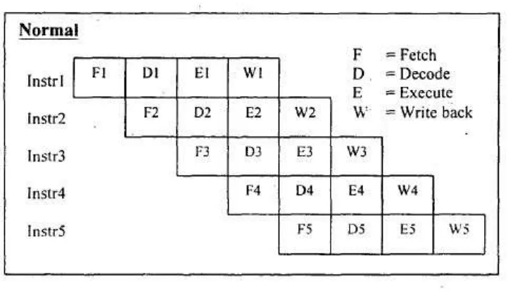
Figure 2-1 The 4-Stages Super-Pipeline of Pesona
Refer to figure before, the 4-Stages Super-Pipeline of Pesona which consist of fetch, decode, execute and write back is needed to increase the speed of processing instruction. All the decomposition of the instruction processing as below;
• Fetch – Read the next expected instruction • Decode – Determine the opcode and the operand
• Execute – Perform the operation and stored in specific destination • Write Back – Store the result in memory
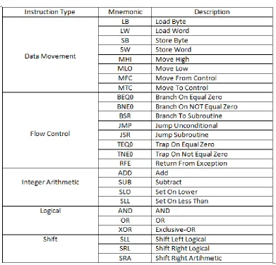
Pesona Microprocessor has 26 instructions set that support two addressing modes i.e. direct addressing and indirect addressing. The instructions set are divided into five groups like data movement, program and system control, integer and logical arithmetic and data shifting as shown on Table 2-1.
6
Table 2-1 bundle the instruction by type which can create more understanding on the instruction set of Pesona. All mnemonic of the instruction set are clearly explained on the description such as MHI which the instruction to move high bit data into register.
PI6 is suitable for used in microcomputer system development with minimum configuration; it is easier to develop and gives more choice to designer for peripherals selection and choosing from different processor family [2].
7
2.2 Processor in Field Programmable Gate Array (FPGA)
Field Programmable Gate Array (FPGA) is an integrated circuit that has been designed to be configured by user. The configuration of it is exclusively done by using the Hardware Description Language (HDL). The Field Programmable Gate Array (FPGA) is a programmable digital logical chip that can be programmed to do almost any digital function.
The processor consist of a collection of a logic cells called lookup tables (LUTs) that act as a small Random Access Memory(RAM) which can implement any logic function. Each other logic cell can be connected with each other through interconnection resources.
They are two types of FPGA processors which are soft core processor and hard core processor. Soft core processors are implemented or programmed into the FPGA fabric while the hard core one is implemented similar to any integrated circuit as a structure in the FPGA fabric. In this case, a soft core processor have been implemented through instruction sets, arithmetic-logic units, register files, and other features specifically tailored to efficiently use FPGA resources.
A soft core processor can be changed and the code can be modified simply by reprogramming the physical FPGA device with a modified hardware design or upgrading the embedded code in it. So, it could lead to a true field upgradeable hardware and software.
8 MicroBlaze
This soft core processor in Figure 2-2 is based on Xilinx FPGA which uses a 32-bit of Harvard architecture soft processor. Advanced architecture like AXI interface, Memory Management Unit (MMU), instruction and data-side cache, configurable pipeline depth and Floating-Point unit (FPU) are supported by this processor.
MicroBlaze contains over 70 user-configurable options, enabling virtually any processor use case from a very small footprint state machine or microcontroller to a high performance compute-intensive microprocessor-based system running Linux, operating in either 3-stage pipeline mode to optimize size, or 5-stage pipeline mode to optimize speed delivering faster Dhrystone Million Instructions Per Second (DMIPS) performance than any other FPGA-based soft-processing solution.