American Journal of Engineering Research (AJER)
e-ISSN : 2320-0847 p-ISSN : 2320-0936
Volume-02, Issue-09, pp-163-170
www.ajer.org
Research Paper Open Access
Design the High Gain and Low Power Amplifier for Radio over
Fiber Technology at 2.4 GHz
A. Salleh, N. R. Mohamad, M. Z. A Abd Aziz, M. N. Z Hashim, M. H. Misran,
M. A. Othman
1,2,3,4,5,6Center for Telecommunication Research & Innovation (CeTRI), Faculty of Electronic & Computer Engineering(FKEKK), Universiti Teknikal Malaysia Melaka (UTeM), Hang Tuah Jaya, Melaka, Malaysia
Abstract:- This paper describes the high performance design a power amplifier for Radio over Fiber (RoF) Technology at 2.4 GHz using Agilents HBFP-0450 transistor. Based on wireless network RoF technology has been proposed as a promising cost effective solution to meet ever increasing user bandwidth and wireless Advanced Design System (ADS) software . The design has shown an acceptable behavior with gain of 13.172 dB. At the 1-dB compression point the output power is approximately 16.108 dB and the Power Added Efficiency (PAE) is 24.915 %.
Keywords: - Power Amplifier, Radio Access Point, Radio over Fiber, Advanced Design System (ADS), Gain
I. INTRODUCTION
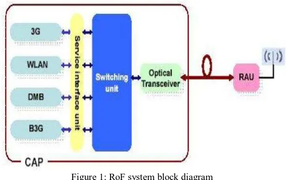
RoF is refers to a technology whereby light is modulated by a radio signal and transmitted over an optical fiber link to facilitate wireless access [1]. RoF is a well established technology that used intensively worldwide for delivering radio signal from a CS to RAPs via an optical fiber [2]. Recently, wireless communication is becoming an integral part of today‟s society. The proliferation of mobile and other wireless devices coupled with increased demand for broadband services are putting pressure on wireless systems to increase capacity. To achieve this, wireless systems must have increased feeder network capacity, operate at higher carrier frequencies, and cope with increased user population densities. However, raising the carrier frequency and thus reducing the radio cell size leads to costly radio systems while the high installation and maintenance costs associated with high-bandwidth silica fiber render it economically impractical for in-home and office environments [3]. With such advantages of optical fiber as low loss, large bandwidth and transparent characteristics, RoFs system can simultaneously support multi-standard applications including cellular services and Wireless Local Area Networks (WLANs) [4]. 2.4 GHz frequency is one most commonly used license free frequencies which based on IEEE802.11 standard for WLAN. RoF systems are expected to play an important role in future wireless communication and phased array antenna sensor systems [5-8].
Inter-system interference is therefore an important issue if there is overlap between signals from one system and the harmonics of another. Such a situation arises for example between GSM900 and DCS1800. Second order distortion is therefore the main limitation of dynamic range in this situation [1]. A power amplifier is placed between the EAM and the antenna in order to improve the dynamic range of passive pico cell (RAP). Pico cells use low power and low capacity base stations that are small, light, relatively low cost and easy to install [2]. Pico cell has a coverage range up to 100 m. To achieve this distance, the RAP needs to operate in active mode, by inserting RF amplifier between optoelectronic photo detector and antenna for downlink path, and inserting LNA between the antenna and optoelectronic modulator [9]. Fig. 2 shows the simple diagram representation of an active optical RAP. Due to a bi-directional amplifier is needed to provide amplification in both transmit and receive directions, the microwave circulators or similar devices will be needed to provide separate uplink and downlink signal paths between the EAM and the antenna. Likely the power amplifier of general RF system, amplifier design for RoF involves many tradeoffs between noise figure, gain, linearity, impedance and matching network [10].
Figure 1: RoF system block diagram
Figure 2. Active Optical Radio Access Point
II. DESIGNMETHODOLOGY
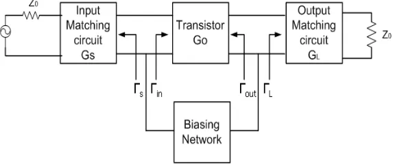
Designing a power amplifier consist of different steps which based on conjugate matching method. The maximum gain or conjugate matching method is in the single stage amplifier design. This method will be realized when the overall gain given by a transistor, Go provide a conjugate match between the amplifier source
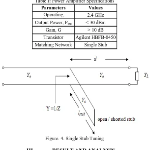
or load impedance and the transistor as shown in Fig. 3. A critical step in any power amplifier design is the selection of transistor. The transistor used in the current design is Agilent HBFB-0450. This product is based on a 25 GHz transition frequency fabrication process, which enables the products to be used for high performance, medium power, and low noise applications up to 6 GHz. The microwave bipolar transistor is usually of the non type and are often preferred over GaAs field effect transistor (FET) at frequencies below 2 to 4 GHz because of the higher gain and lower cost [12]. Table 1 shows the specifications of the power amplifier (PA) design. The operating frequency of the amplifier is at 2.4 GHz. The target of this project is that design the low power of PA which for short range application (pico cell). The output power of pico cell is less than 1 Watt (30 dBm) and the maximum output power produced at WLAN 2.4 GHz is 20 dBm [13].
First of all a DC simulation must be done to find the optimal bias and bias network for the system. From the transistor datasheet, it concern to choose the biasing point which produced the best performance in term of gain. The gain of the transistor is depending on the S parameter at the operating frequency. Biasing is a process to obtain the transistor static IV curves for desired operation such as class A, class B, class C, or class AB. The biasing point at VCE= 3 V and IC = 50 mA is selected because have higher gain compare to the others
biasing point. The higher value of S21(dB) can give a higher gain. Next, S-parameter simulations is done to find
the exact value of the S-parameters and evaluate the stability of the model at the operating point. When embarking on any amplifier design it is very important to spend time checking on the stability of the device chosen, otherwise the amplifier may well turn into an oscillator. The main way of determining the stability of a device is to calculate the Rollett‟s stability factor (K) based on a set of S-parameters for the device at the frequency of operation [12]. There are two stability parameters K and |Δ| is used to indicate that whether a device is likely to oscillate or not or whether it is conditionally or unconditionally stable.
Figure. 4. Single Stub Tuning
III. RESULTANDANALYSIS
The first step towards designing the class A power amplifier was to select a suitable bias point for the operation. The transistor should be biased for class A operation and maintained comfortably inside the rectangle limited by the nonlinearity borders which are the collector-emitter voltage, Knee voltage, Vk, and collector-base
breakdown, VBR. Transistor I-V curves with the optimal load line for the class A operation is shown in Fig. 5.
The bias point at the optimal condition is Vce = 2.45 V and Ic = 40.35 mA. The I-V curves also help to see a
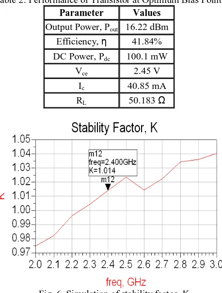
safety region which condition that the device can be expected to operate without self-damage due to thermal heating. The performance of transistor at the optimal bias value is summarized in Table 2. The maximum output power of this transistor is 16.22 dBm which the transistor can be used for pico cell application (less than 20 dBm).
The main way of determining the stability of a device is to calculate the Rollett‟s stability factor (K),
which is calculated using a set of S-parameters for the device at the frequency of operation.. The stability can be determined from the value of K and ∆. The simulation of stability is shown in Fig. 6. The system is the unconditional stability due to |Δ| < 1 and K > 1 which mean that the amplifier is stable for all passive sources and load impedance. After the stability of the transistor have been determined, and the stable regions for the reflection coefficient for source and load (ΓS and ΓL) have been located on the Smith chart, the input and output
Figure. 5 I-V curves.
Table 2: Performance of Transistor at Optimum Bias Point.
Parameter Values
Output Power, Pout 16.22 dBm
Efficiency, η 41.84% DC Power, Pdc 100.1 mW
Vce 2.45 V
Ic 40.85 mA
RL 50.183 Ω
Fig. 6. Simulation of stability factor, K .
The single stub matching technique is used to obtain the input and output matching. From this matching technique, the distance,
d
and length of stub,
are acquired which open circuit shunt stub is used to find the length of stub. Fig 7 shows the schematic of the input and output matching. The distance and length of stub which obtained from the Smith chart are converted to micro-strip line. The transformation to the micro-strip lines (MLIN and MLOC) are obtained by using an ADS Line calculator, LineCalc. The shunt tuning is especially easy to fabricate in microstrip or stripline form. The matching network can easily be determined using the Smith chart. For the shunt- stub case, the basic idea is to select the distance, d so that admittance, Y, seen looking into the line at d from the load is of the form Y0 + jB. Then the stub susceptance is chosen as –jB,Figure. 7. Schematic of Input and Output Matching
The optimization of input and output matching is needed to improve the performance of the amplifier. The width and length of micro-strip line are tuned until the magnitude of S11 and S22 approximately to zero
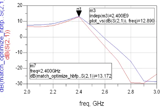
which for the perfect matching. The magnitude of both S-parameters are referred to the reflection coefficient, Γ at the input and output. Fig. 8 shows the comparison of gain before and after optimization. From the observation, all the parameter presented the improvement. For example, the gain of amplifier was increased from 12.89 dB to 13.172 dB. The aim of optimization is to improve the performance of an amplifier such as the gain, input and output return loss. For example, in the simulation using ADS software, tune parameter is used to tune the input (magnitude of S11) and output matching (magnitude of S22). Both of magnitudes are referred to the
reflection coefficient, Γ which for the perfect matching, the value of Γ should be equal to zero.
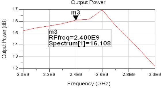
The single tone harmonic balance simulation was done to plot the transducer power gain, the PAE, input power, Pin, and output power, Pout. Fig. 9 shows the transducer power gain versus frequency. The gain
increases a frequency increases until 2.6 GHz. Then, after that frequency, the gain decreases as a frequency increases. At a 1-dB compression point, the gain is 9.012 dB at 2.4 GHz. The input 1-dB compression point is defined as the power level for which the input signal is amplified 1 dB less than the linear gain. When a power amplifier has operated in its linear region, the gain is a constant for a given frequency. However when the input signal power is increased, there is a certain point beyond which the gain is seen to decrease. Fig. 10 shows the relationship between PAE and frequency. PAE is directly proportional to output power, it takes a maximum value of 32.132 at 11 dBm input power and it takes a value of 24.951 at the 1-dB compression point. Fig. 11 shows the Pout vs. frequency which the response has same characteristic with the Fig 10. The output power is
about 16.108 at 1-dB compression point.
Figure. 9. Transducer power gain versus frequency
Figure. 10. Power Added Efficiency Vs. Input Power
Figure. 11. Output power vs. frequency
IV. CONCLUSION
VI. REFERENCES
[1] P P Smyth, Optical Radio – A review of a Radical New Technology For Wireless Access Infrastructure, In: Peter Smyth. Mobile and Wireless Communication: Key Technologies and Future Applications. London. : The Institution of Electrical Engineers. 2004.
[2] Vanblaricum, M.L. , Photonic Systems for Antenna Applications, IEEE Antenna Propag. Mag, 36(5), pp. 30-38, 1994.
[3] A. Salleh, M. Z. A Abd Aziz, N. R. Mohamad, M. A. Othman, Z. Zakaria, M. H. Misran, “Design of Low Noise Amplifier for Radio over Fiber Technology at 5.2 GHz”, IOSR Journal of Electonics and Communication Engineering , vol. 5, issue 3, pp. 65-69, 2013.
[4] Hyo-Soon Kang, Myung-Jae Lee and Woo-Young Choi, Multi Standard Radio over Fiber Systems using CMOS-Compatible Si Avalanche Photodetector, Asia Pacific Microwave Photonics Conference, pp. 302–35, 2008.
[5] Hamed Al-Raweshidy, Shozo Komaki, Radio over Fiber Technologies for Mobile Communications Networks, Artech House, Boston, 2002.
[6] P.K.Tang, L.C.Ong, B.Luo,A.Alphones and M.Fujise, Transmission of Multiple Wireless Standards over a Radio-over-Fiber Network, IEEE Microwave Symposium Digest ,2004.
[7] Sangil Kim, Hodeok Jang et al, Performance Evaluation for UWB Signal Transmission with Different Modulation Schemes in MultiCell Enviroment Distributed Using ROF Technology, 2004.
[8] Gurprakash Singh and Arokiaswami Alphones, OFDM Modulation Study for Radio-over-Fiber System for Wireless LAN (IEEE802.11a), 4th International Conference on Information, Communications & Signal Processing , 2003.
[9] Razali Ngah, Teguh Prakoso & Tharek Abdul Rahman, Coverage Range and Cost Comparison of Remote Antenna Unit Designs for In building Radio over Fiber Technology, ITB J. ICT Vol. 2, No. 1, 2008.
[10] Pengcheng Xiou, Zhigong Wang, 5.2GHz CMOS Narrow Optical Receiver for Radio over Fiber,Proc. of International Conference on Communications, Circuits and Systems, pp. 1937-1941, 2006.
[11] Muthuswamy Venkataramani, Efficiency Improvement of WCDMA Base Station Transmitters using Class-F power amplifiers, Virginia Polytechnic Institute and State University, Feb 2004.
[12] D. M. Pozar, Microwave and RF Design of Wireless Systems, John Wiley & Sons, Inc., 2001.
[13] Westbrook, L.D. and Moodie, D.G., „Simultaneous bidirectional analogue fibre optic transmission using