Keywords: RF, Front End Receiver, WiMAX
Abstract
This paper presents the design of a high gain, low noise direct conversion Radio frequency(RF) front-end receiver system. The Front end receiver is designed to operate at 5.8 GHz compliant with IEEE 802.16 WIiMAX standard. The system consists of a low noise amplifier (LNA), a radio frequency amplifier (RFA), a power divider and two band pass filters. The overall performance of the RF front-end receiver system produced a gain of 52.4 dB. A cascaded LNA designed for the system produced a high gain of 36.8 dB. The RFA contributed an extra gain 15.6dB. The overall noise figure achieved for the system is 3.7 dB. The return loss achieved is -25.5 dB for the RFA. The radio frequency bandwidth recorded for the system is above 1120 MHz. The measured power divider insertion loss is 2.80 dB. Using microstrip technology for designing the Chebyshev filter, the insertion loss is 3.00 dB and the channel bandwidth recorded is 107 MHz which can accommodate 4 sub channels IEEE WiMAX standard.
1
Introduction
A radio frequency front-end is an important part of the receiver as it provides the necessary gain, while introducing minimal noise, to meet the required signal to noise ratio (SNR). A typical RF front-end receiver consists of low noise amplifier (LNA), filter and mixer. The number of circuits added in the front end receiver varies depending on the type of receiver. The design complexity involves a trade-off between noise, gain and size. A key step in arriving at a cost effective and timely solution is by choosing the proper technology for the RF front-end portion of the radio receiver. Factors that are considered into making decision are for example: the amount of signal content to be integrated, the application performance requirements and the capabilities of the chosen device. Currently, CMOS and GaAs are both widely used devices for many RF front end receiver design. Questions remain over which technology is most appropriate and the performance trade-offs seen in
migrating between technologies. Uncertainty remains due to differences between architectures, system specifications and circuit designer themselves [1].
An RF front-end receiver for a WiMAX ODU unit would have to be designed for desired frequency, gain, bandwidth and noise figure. The system includes RF components such as a low noise amplifier (LNA), RF amplifier (RFA), power divider and filters. In an RF front-end design, the problem such as noise must be determined and reduced. Multiple parameters such as gain and noise in the RF components for the front-end receiver would have to be compensated. These trade-offs are the challenges that RF designers have to consider in getting a high performance communication system. The system developed should comply with the 802.16 WiMAX standards. A review of this standard is necessary in order to understand the requirements before designing an RF front-end receiver. The review below will focus on circuit parameters required in designing the RF front-end receiver.
2 IEEE 802.16 Fix Station WiMAX Standard
WiMAX, also known as IEEE 802.16 standard, is a wireless digital communication system that is intended for wireless metropolitan-area network technology that provides interoperable broadband wireless connectivity to fixed, portable and nomadic users [2]. It provides up to 50-kilometers of service area for fixed station and 5-15km for mobile station. It allows users to get broadband connectivity without the need of direct line of sight to the base station, and provides total data rates of up to 70Mbps. It has enough bandwidth to simultaneously support hundreds of businesses and homes with a single base station. The term WiMAX has become synonymous with the IEEE 802.16 Wireless Metropolitan Area Network (MAN) air interface standard. A WiMAX compliant system would provide a cost effective broadband access to users at home, in the office, in areas served by wire-line Digital Subscriber Line (DSL), cable services and to users equipped with portable devices like laptops, Personal Digital Assistance (PDAs) and smart-phones [3].
Table 1 shows the comparison between WiMAX, and its predecessors, the WLAN and Bluetooth technologies. The
RF Front End Receiver for WiMAX Application
Othman A. R, Hamidon A. H, C Wasli, Mustaffa M. F, Ting J. T. H
Faculty of Electronic & Computer Engineering Universiti Teknikal Malaysia Melaka (UTeM)
Locked Bag 1600, Hang Tuah Jaya, Ayer Keroh, Melaka,
Malaysia
table compares the three different standards in term of frequencies, communication distance, data transfer rates and number of users for each system. It also shows that WiMAX system is an evolution of WLAN and Bluetooth technologies. The frequency varies from 2.4 GHz for standard WLAN to 11 GHz for WiMAX standard. The communication distance for WiMAX can be extended to 50 km.
Parameters 802.16a (WiMAX)
802.11 (WLAN)
802.15 (Bluetooth) Frequency
Band
2-11 GHz 2.4 GHz Varies Range ~50 km (31
miles)
~100 meters
~10 meters Data transfer
sate
70 Mbps 11Mbps ~ 55Mbps
20 Kbps ~ 55Mbps Number of
users
Thousands Dozens Dozens
Table 1: Comparison between WiMAX, WLAN and Bluetooth
3 Radio Frequency Receiver Architecture
Recent advances in wireless networking technologies, including 1-1.8GHz cellular phone, 1.9-2.2 GHz W-CDMA, and 2.4-5.2GHz WLAN/HiperLAN have urged development of low-cost, low-power, and small-size multifunctional RF system [4]. In addition, to facilitate a global location free access and personal mobility, integration of these services is crucial and requires development of multimode front-end modules capable of switching from one service operating at a frequency to another service operating at another frequency. A currently available multimode approach makes use of different chips for different modes and therefore does not meet low cost low, low power and small size requirement [5]. Another available approach applies the same chip, but has an inter-mode multiple frequency relation constraint.
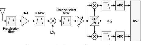
Figure 1 shows a typical heterodyne receiver. It consists of an antenna coupled directly to a pre-selection filter before passing through a low noise amplifier.
Figure 1: Typical Heterodyne Receiver
After passing through an image rejection filter(IR) the signal is mixed with a local oscillator (LO) and down converted to an intermediate frequency (IF). It is again filtered before being further amplified through a variable gain IF amplifier. The signal is then split and mixed with a second oscillator to produce a baseband signal for further processing. Figure 2 shows a direct conversion receiver.
Figure 2: Typical Direct conversion Receiver The difference between direct conversion receiver and the heterodyne receiver is that the direct conversion receiver does not require the IR filter, the RF mixer, an RF local oscillator and a channel select filter. The direct conversion receiver does not require a down conversion circuit.
4 Front End Receiver Design
Most of the front-end receivers developed were for license and unlicensed band of frequencies between 4.9 to 5.89 GHz. The maximum reported gain achieved was 32 dB with overall noise figure between 1.5 to 5.8 dB.
Figure 3: Proposed new front-end receiver.
The overall front-end receiver should introduce a higher gain of 50 dB compared to the 32 dB reported from the literature review, by taking into consideration the extension of communication distance of up to 50 km. To maintain a noise figure of less than 10 dB for the overall system as recommended by IEEE 806.12 WiMAX standard the noise figure for the front-end receiver should not exceeded -5 dB. Since the system should be capable of offering a higher capacity of subscribers of up to 200 channels, the bandwidth should be 800 MHz. This is double the standard 400 MHz for 20 sub-carrier of 20 MHz each. The input sensitivity of the system should cover the minimum sensitivity of -80 dBm.
5 LNA and RFA
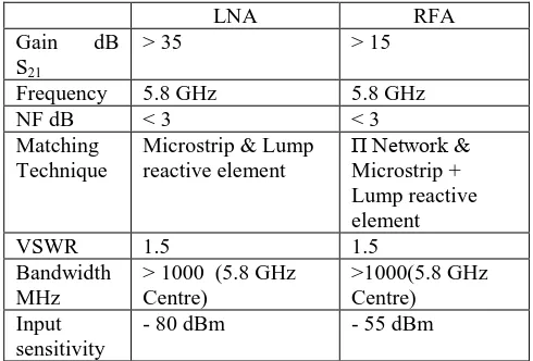
should be less than 3 dB The approach taken in designing the amplifiers involves a series of chronological steps. No design is complete without some desired goals. The design specifications for the low noise amplifier and the targeted S parameter for the LNA and RFA are shown in Table 2 and Table 3.
LNA RFA
Gain dB S21
> 35 > 15
Frequency 5.8 GHz 5.8 GHz
NF dB < 3 < 3
Matching Technique
Microstrip & Lump reactive element
Π Network &
Microstrip + Lump reactive element
VSWR 1.5 1.5
Bandwidth MHz
> 1000 (5.8 GHz Centre)
>1000(5.8 GHz Centre) Input
sensitivity
- 80 dBm - 55 dBm
Table 2: Design specifications for LNA and RFA
Table 3: Targeted S Parameters for LNA and RFA
6 Band Pass Filter
Two bandpass filters with center frequencies 5.75 GHz and 5.85 GHz are required. Each of these filters should have a bandwidth of least 100 MHz. These filters are required to separate the signal into two main channels with four subchannels. Filter design methods include image parameter method and insertion loss method. Image parameter method is featured by master-slave configuration of simple 2-port filters to represent cut-off frequency and attenuation characteristic. Chebyshev (equal-ripple) filter generates some degree of ripple at pass band but shows excellent cut-off characteristics at stop band. Since the critical design factor in this design is fast cut off characteristic at stop band, this filter is chosen. At this frequencies a microstrip line filter, which allow implementation of both compact size and integration is preferred. For this project, a coupled line Chebychev filter is selected.
7 Power Devider
Power divider is a passive microwave device used to divide input power to more than two output ports with lower power
level depending on the number of output ports as shown in Figure 4.
Figure 4: Power Divider
A power divider is ideally a lossless reciprocal device which can also perform vector summation of two or more signals and thus is sometimes called a power combiner or summer. For this project a Wilkinson power divider is adopted.
8 Design and Simulation
Low noise amplifier was design based on the targeted specification listed in previous section. The FET chosen for the design is FXL76LP. The S parameter for the FET is shown in Table 4. These parameters were measured at VDD
= 2 V and IDS = 10 mA which sets the biasing for the FET.
Frequency GHz
S11 S12 S21 S22
5.8 GHz 0.712 0.065 8.994 0.237 Table 4: S-parameter from Transistor FHX76LP datasheet The overall performance of the low noise amplifier is determined by calculating the transducer gain GT, noise
figure F and the input and output standing wave ratios, VSWRIN and VSWROUT. The optimum,
Γ
optandΓ
L were obtained asΓ
opt= 17.354 +j 50.131 andL
Γ
= 79.913- j7.304. The calculated gain for the LNA was 19.3 dB, which correspond to a noise figure of 0.301 dB. The input matching loadΓ
opt is required to provide high-loaded Q factor for better sensitivity. A T-network was used to match the input impedance (Bhartia, 2003a). The elements of T-network can be realized in the form of lump reactive elements and microstrip line impedance. The resultant matching component values are given in Table 5.Components Values
L1 3.60 nH
L2 0.88 nH
L3 0.67 nH
L4 0.75 nH
C1 0.5012 pF
CB 7.5 pF
Table 5: LNA Amplifiers Parameters
With these components, the schematic circuit for the single stage LNA is shown in Figure 5. This circuit was redrawn and simulated using Ansoft Designer to fine tune and further optimization for a better performance.
S Parameters LNA RFA
Input reflection S11 dB -10 -10
Return Loss S12 dB -10 -10
Forward Transfer S21
dB
35 15
Output Reflection loss S22 dB
-10 -10
Figure 5: The schematic circuit for single stage amplifier
The RF amplifier was designed based on the specification listed in previous section. The design of the RF amplifier follows the same procedure used in designing the LNA. Using theoretical design equations for the RFA, the equations are computed using MathCad. The FET chosen for the design is EPA018A. The S parameter given for the FET is shown in Table 6. These parameters were measured at VDD = 2 V and IDS = 10 mA which sets the biasing for the
FET. This transistor biasing circuit is similar with the LNA amplifier.
Frequency GHz
S11 S12 S21 S22
5.8 GHz 0.728 0.049 6.327 0.237 Table 6: S Parameters of EPA018 A
Gain, noise figure, input and output matching components were calculated and simulated using MathCad and ADS 2005A. Both calculated and simulated results were almost similar. Hence Table 7 lists both the calculated and simulated results for the RF amplifier. The stability factor as is 0.989. This showed a clear tendency for oscillation which confirmed the calculated stability factor. The calculated transducer power gain for matched condition was 16.28 dB. The input matching for optimum
Γ
optandL
Γ
were obtained asΓ
opt = 12.662 +j 38.168 andL
Γ
= 79.97- j7.286. The noise figure calculated is 2.475 dB.S Parameters Targeted RFA
Calculated and Simulated values Input reflection S11 dB -10 -8.03
Return Loss S12 dB -10 -21.45
Forward Transfer S21 dB 15 15.31
Output Reflection loss S22
dB
-10 -7.85
Noise Figure NF dB * <3 2.47 Bandwidth MHz >1000 >1000 Table 7: Calculated and Simulated Results for Designed RF
Amplifier
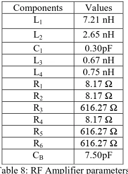
The RF amplifier can also act as an isolator for the overall front-end system and a suitable Π-network with 50 Ώ load impedance was inserted at the input and output of the amplifier to provide a 3 dB insertion loss each for the network. The RF amplifier component with the 3 dB attenuation is shown in Table 8.
Components Values
L1 7.21 nH
L2 2.65 nH
C1 0.30pF
L3 0.67 nH
L4 0.75 nH
R1 8.17 Ω
R2 8.17 Ω
R3 616.27 Ω
R4 8.17 Ω
R5 616.27 Ω
R6 616.27 Ω
CB 7.50pF
Table 8: RF Amplifier parameters
Figure 6 shows the schematic circuit for RF amplifier with associated component and the 3 dB attenuator resistors.
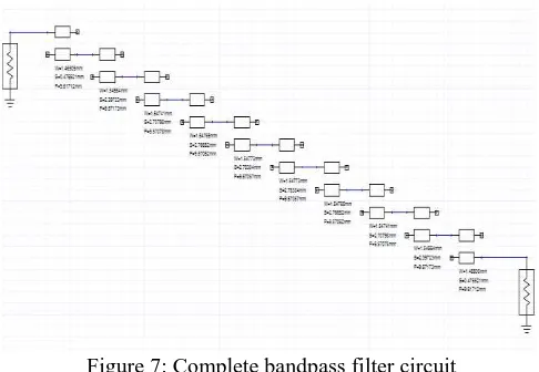
Figure 6: Schematic circuit for RF amplifier The first step to design a bandpass filter is to determine the order of the filter that can work efficiently in the application system based on their design specification. In this project, the filter should be designed to fulfill the required specification for WiMAX application. The design specification for this bandpass filter is shown in Table 9 below
Filter Specification Value Center Frequency 5.75 GH
Filter Type Chebyshev
Insertion Loss S21 <-10 dB
Stopband Attenuation 25 dB @ 5.85 GHz
Bandwidth 100 MHz
Ripple 0.5 dB
Table 9: Bandpass filter design specification
For the filter design, first is to decide the n order of the filter based on the specification shown in Table 9. The order of the filter can be determine from plotting the normalized frequency versus attenuation.
parameters values are acceptable since the required specification for insertion loss is less than -10 dB and reflection loss is more than -10 dB. The bandwidth is measured about 107 MHz.
Figure 7: Complete bandpass filter circuit
The comparison between targeted and simulated parameters result for band pass filter is shown Table 10.
Filter Specification Targeted Value Simulated Value Center Frequency 5.75 GHz 5.75 GHz
Filter Type Chebyshev Chebyshev Insertion Loss S21 <10 dB 3.0 dB
Stopband Attenuation
25 dB @ 5.85 GHz
75 dB @ 5.85 GHz
Bandwidth 100 MHz 102 MHz
Ripple 0.5 dB 0.5 dB
Table 10: Comparison Parameters for Bandpass filter
Two forms of power dividers are generally constructed by cascading two-way dividers. These 2-way dividers are typically either terminated 180° hybrid (for RF frequency units) or Wilkinson or tapered line dividing structures (for microwave frequency devices). These characteristic impedances are then converted to line impedance using LineCalc Program provided in AnSoft Designer software. The power divider design specification is shown in Table 11.
Power divider specification
Value Frequency Range 5.3 to 6.3 GHz
Type Wilkinson
Structure 2-way equal power
Insertion Loss 3.5 dB
Return Loss <-10 dB
Input Return Loss <-10 dB Table 11: Power divider design specification The comparison between targeted and simulated parameters is shown in Table 12. As can be seen that the simulated parameter values are above and better than the targeted values.
.
Power divider specification
Targeted Value SimulatedValue Frequency Range 5.3 to 6.3 GHz 5.3 to 6.3 GHz
Type Wilkinson Wilkinson
Structure 2-way equal power
2-way equal power Insertion Loss S21 3.5 dB 3.14 dB
Return Loss S12,
S13,S31
< -10 dB -17.18 dB Input Return Loss
S11
<-10 dB -25.92 dB Table 12: Comparison between Targeted and Simulated parameter value of Power divider
A final schematic circuit for power divider is simulated as shown in Figure 8 below.
Figure 8: Complete power divider circuit
9 Measurement and Analysis
The result for LNA RF front-end module is presented in Table 13.
Table 13: S Parameter result for LNA
From the tabulated values, the S11 parameter measured is
11.4 dB. This is -1.4 dB less than targeted which is better and acceptable. S22 measured is -12.3 dB which is less than
targeted and acceptable. The return loss required S12
obtained is less than -39 dB. The related measured gain S21
S Parameters Targeted Measured Comment Input Reflection S11
dB
<-10 -12.4 Achieved Return Loss S12 dB <-10 -25.5 Achieved
Forward transfer S21 dB
>15 15.6 Achieved Output
ReflectionS22 dB
<-10 -12.3 Achieved
NF dB * <3 2.4 Achieved
for the LNA amplifier is 36.8 dB. The noise figure values obtained is 1.37 dB which complied with the targeted value of less 3 dB. The use of T lump reactive element and microstrip line matching technique at the input of the LNA contributes the best performance for the amplifier.. This matching technique was used to provide high-loaded Q factor for better sensitivity and thus minimized the noise figure. The elements of T-network were realized in the form of lump reactive elements and microstrip line impedance. The 3 dB bandwidth for the amplifier is measured using setup Figure 5.3a. The 3dB bandwidth obtained is 1.24 GHz compliant with targeted result of more than 1 GHz.
Table 14: S Parameter results for RFA The RF amplifier measurement setup is similar to the measurement set up for LNA. The results are shown in Table 14.
From the tabulated values, the S11 parameter measured is
-12.4 dB. This is -2.4 dB less than targeted which is better and acceptable. S22 measured is -12.3 dB which is less than
targeted and acceptable. The return loss required S12
measured.. The noise figure values obtained is 2.4 dB which complied with the targeted value of 3dB. Again shows that the use of T lump reactive element and microstrip matching network provide best performance for the RFA since the measure value nearly optimized. The 3dB bandwidth obtained is 1125 MHz which is more than the targeted result of 1000 MHz.
Measurements for power divider were also carried out. The measurement setups as LNA and RFA were used to measure the related parameters shown in Table 15.
The measured insertion loss for the power divider is -2.73 dB. This is better than the targeted insertion loss of -3.5 dB. The measured S12, S13, and S31 are 18.54 dB and related
return loss S11 is -22.23 dB.
Table 15: Power Divider Results.
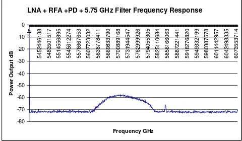
Setup of LNA and RFA were also used to measure the filter parameters. The result for the filter is tabulated in with center frequency 5.75 GHz. The output from the filter is shown in Figure 9.
LNA + RFA +PD + 5.75 GHz Filter Frequency Response
-80
5452446138 5483501517 5514556895 5545612274 5576667653 5607723032 5638778411 5669833790 5700889168 5731944547 5762999926 5794055305 5825110684 5856166063 5887221441 5918276820 5949332199 5980387578 6011442957 6042498335 6073553714
Frequency GHz Figure 9: Power output vs Frequency GHz for LNA +
RFAmp + Power Divider + Filter S Parameters Targete
d
Measure d
comment Input Reflection S11
dB
<-10 dB -11.4 Achieved . Return Loss S12 dB <-10 dB -39.1 Achieved
Forward transfer S21
dB Type Wilkinson Wilkinson Structure 2-way
Return lossS11 -10 dB -22.23dB Achieved
An additional power drop of -4.2 dB was observed. This was expected considering losses contributed by the connector of 1.2 dB. The insertion loss calculated is 3.00 dB. Adding another filter of center frequency 5.85 GHz, the output response is shown in Figure 10.
5.85 GHz Filter Frequency Response
5450279483 5479168208 5508056932 5536945657 5565834381 5594723106 5623611830 5652500555 5681389279 5710278004 5739166728 5768055453 5796944177 5825832902 5854721626 5883610351 5912499075 5941387800 5970276524 5999165249 6028053973 6056942698
Frequncy GHz
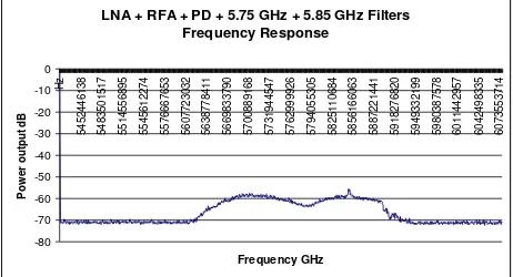
Figure 10: Power output vs Frequency GHz for LNA + RFAmp + Power Divider + Filter (5.85GHz) As expected the frequency response of the filter gave a center frequency of 5.85 GHz with bandwidth of 102 MHz. The insertion loss for the filter is 7.2 dB. The output
5452446138 5483501517 5514556895 5545612274 5576667653 5607723032 5638778411 5669833790 5700889168 5731944547 5762999926 5794055305 5825110684 5856166063 5887221441 5918276820 5949332199 5980387578 6011442957 6042498335 6073553714
Frequency GHz
Figure 11: Power output vs Frequency GHz For LNA + RFAmp + Power Divider + Filter (5.75GHz+ 5.85 GHz) The output response shows the total bandwidth for the system to be about 212 MHz as expected for two channel bandwidth.
The Front-end system designed consisted of a LNA, RFA, Power divider and filters are developed. The final result for overall amplifier gain is 52.40 dB gain with noise figure of 3.70 dB. The total insertion loss for the front-end is 5.80 dB which is contributed by passive network power divider and filters. With injecting a -80 dBm signal at the input of the front-end receiver, an output power of -59 dBm is achieved at the output. With considering the attenuation set at the spectrum analyzer, the actual signal output at the RF front-end receiver is -39.00 dBm. For a wireless communication system such as WiMAX system, this RF front-end receiver will capable to provide a better pipeline for the receiver with minimum noise figure and provide a high gain. This output is acceptable for further processing of the baseband system for IEEE 802.16 WiMAX standard.
10 Conclusion
A proposed direct conversion front end receiver system consists of Low noise amplifier (LNA), radio frequency which is used in the system produces a high gain of 36.8 dB. The RFA contributes 15.6dB gain which is higher than the targeted of 15 dB. The implementation of T matching network for the LNA and the RFA that uses microstrip and lumped reactive element matching network gives a good overall performance of gain and noise figure for the system. Two 3 dB attenuators were inserted at the input and output RFA for system to isolate the system from the reflected load power also shows an improvement in return loss of the overall system. The radio frequency bandwidth recorded for the system is above 1000 MHz which complies with the targeted bandwidth. Using microstrip line technology for designing the filter, the channel bandwidth recorded is 107 MHz which can accommodate 4 sub channels. The front-end system developed can be implemented in IEEE 802.16 WiMAX standard with the standard input sensitivity of -80dB and channel bandwidth.
References
[1] Ickjin Kwon, Yunseong Eo, Seong-Sik Song, Kyudon Choi, Heungbae Lee & Kwyro Lee. A Fully Integrated 2.4-GHz CMOS RF Transceiver. IEEE 802.15.4. [2] Roger Marks (2004). IEEE standard 802.16: A
Technical Overview of a WirelessMAN Air Interface For Fix Broadband Wireless System. IEEE 802.16 Working Group, 2004.
[3] IEEE Computer Society and IEEE Microwave Theory Technique and Society (2004) Part 16 Air Interface For Fix Broadband Wireless System, IEEE Standard 802.16 -2004.
[4] M Madihan. (1999). C MOS RF IC,s for 900 MHz- 2.4 GHz band wireless communication networks. Proceedings of the RFIC symposium, pp 13 – 16 , June 1999.