i
MULTIPLE PHASE SHIFTER DESIGN BY USING PIN DIODE FOR MIMO APPLICATION
NURUL HARYANI BINTI YAACOB
This report is submitted in partial fulfillment of the requirements for the award of Bachelor of Electronic Engineering (Telecommunication Electronics) With Honours
Faculty of Electronic and Computer Engineering Universiti Teknikal Malaysia Melaka
ii
“I hereby declare that this report is the result of my own except for quotes as cited in
the references.”
Signature
Author
Date
:
: NURUL HARYANI BT YAACOB
iii
“I hereby declare that I have read this report and in my opinion this report is
sufficient in terms of the scope and quality for the award of Bachelor of Electronic
Engineering (Telecommunication Electronics) With Honours.”
Signature
Supervisor’s Name
Date
:
: MOHAMAD ZOINOL ABIDAIN ABD AZIZ
iv
DEDICATION
Special dedication belongs to my beloved parents, Yaacob Mariman and
Norraini Lamin. My special thanks to my kind hearted supervisor Mohamad Zoinol
Abidin Abd Aziz, all lecturers in faculty of electronics and computer engineering and
v
ACKNOWLEDGEMENT
My deepest gratitude goes to my supervisor Mohammad Zoinol Abidin Abd
Aziz, for his guidance, support, helpful comments and the knowledge in doing this
thesis. Lots of love from deepest of my heart goes to my family especially my
parents whom always given me their love and warm support. I am grateful to all of
my lecturers and friends for helping directly or indirectly in the completion of my
thesis.
vi
ABSTRACT
This project presents a Multiple Phase Shifter Design by using PIN Diode for
MIMO Application. Multiple Phase Shifter design is a method, where to differentiate
multiple signal and the interferences. Besides, it is also to increase the performance
channel and to improve the data rate. The multiple phase shifter circuit is designed
with consist multiple input multiple output. PIN diode is used as a switch. The
Multiple Phase Shifter 4x4 is designed to produce various output signals with
different phase at 2.4GHz frequency. The designed methods are used to complete the
project included calculation and simulation. Calculation method is done to obtain the
width, W and the length, L of phase shift for each phase angles. Simulation method is
done to design the phase shifter circuit by using Microwave Office 2006 software.
The simulation design constructed based on desired phase shift, which are begin with
simulation for single input single output, single input multiple output and multiple
input multiple output. These design focused on certain different phase; 0°, 45°, -45°,
90°, -90°, 135°, 180°/-180° and 360°. The magnitude for return loss for each port in
input port around -20dB and the isolation for every port is more than -3dB. The beam
rosette pattern is changing based on the phase different in output. The analysis that
had been done is the more length, L of the phase shift caused the different phase
greater than or smaller than. The size of the layout of phase shift was 20.08mm in
vii
ABSTRAK
Projek ini adalah sebuah penganjak fasa berbagai yang menggunakan diod
PIN untuk aplikasi MIMO. Perisian gelombang mikro (AWR) digunakan untuk
merekabentuk litar yang mempunyai berbagai masukan dan keluaran dengan
penggunaan diod PIN sebagai suis. Binaan litar ini adalah untuk mendapatkan hasil
keluaran berbagai fasa yang berbeza pada frekuensi 2.4GHz. Kaedah yang digunakan
untuk merekabentuk dengan melakukan pengiraan dan simulasi. Kaedah pengiraan
digunakan untuk mendapatkan nilai ketebalan dan panjang jalur penghantaran setiap
sudut. Kaedah simulasi dilakukan untuk merekabentuk litar menggunakan perisian
Microwave Office 2006. Simulasi ini melalui tiga peringkat iaitu rekaan dengan satu
masukan satu keluaran, satu masukan banyak keluaran dan banyak masukan banyak
keluaran. Rekabentuk litar ini fokus pada beberapa beza fasa; 0°, 45°, -45°, 90°, -90°,
135°, 180°/-180° dan 360°. Kehilangan pergi balik bagi setiap masukan adalah
sekitar -20dB, manakala sisihan adalah lebih daripada -3dB. Bentuk sinaran roset
berubah mengikut beza fasa pada keluaran. Analisa yang di buat adalah kepanjangan
anjak fasa akan menyebabkan beza fasa semakin berubah menjadi semakin
bertambah atau semakin berkurang. Saiz rekaan adalah dengan panjang sebanyak
viii
CONTENTS
CHAPTER TITLE
PROJECT TITLE
STATUS FORM
DECLARE
SUPERVISOR’S DECLARE
DEDICATION
ACKNOWLEDGEMENT
ABSTRACT
ABSTRAK
CONTENTS
LIST OF TABLE
LIST OF FIGURE
LIST OF ABBREVIATIONS
LIST OF APPENDIX
I INTRODUCTION
1.1 Project Background
1.2 Objective of Project
1.3 Problem Statement
1.4 Scope of Project
PAGE
i
ii
iii
iv
v
vi
vii
viii
ix
xii
xiii
xv
xvii
1
2
2
ix
II BACKGROUND STUDY
2.1 Phase Shifter
2.1.1 Hybrid Coupler Phase Shifter
2.1.2 Direct Transmission Loaded Line Phase
Shifter Switched Line Phase Shifter2.1.3
2.1.4 Rotary Phase Shifter
2.2 Diode
2.2.1 PIN Diode
2.2.2 Schottky Diode
2.3 Multiple Input Multiple Output (MIMO) System
2.3.1 Multi-Antenna Types
2.4 Planar Transmission Line
2.4.1 Microstrip Line
2.5 Beamforming
2.5.1 Array Factor Calculation
3 4 5 5 6 7 7 9 11 12 13 15 18 19
III MULTIPLE PHASE SHIFTER DESIGN
3.1 Introduction
3.2 Design of Multiple Phase Shifter
3.2.1 Design Calculation of Multiple Phase
Shifter Simulation of Multiple Phase Shifter3.2.2
21
22
22
23
IV RESULT ANALYSIS AND DISCUSSION
4.1 Simulation Result Analysis
4.1.1 Single Input Single Output Circuit
4.1.2 Single Input Single Output with PIN Diode
Integrated Circuit
4.1.3 Single Input Multiple (3 Ports) Output with
PIN Diode Integrated Circuit
32
32
34
x
4.1.4 Multiple Phase Shifter Circuit 38
V CONCLUSION
5.1 Recommendation 45
47
53
REFERENCES
xi
LIST OF TABLE
NO
3.1
4.1
4.2
4.3
4.4
4.5
4.6
4.7
TITLE
Design Specification Phase
Isolation, Return Loss and Phase Shift Single Input
Single Output at 2.4GHz
Isolation, Return Loss and Phase Shift Single Input
Single Output with PIN Diode Integrated at 2.4GHz
Phase Shift Single Input Multiple Output with PIN
Diode Integrated at 2.4GHz
Phase Shift and Phase Different of Multiple Phase
Shifter at 2.4GHz
Isolation and Return Loss of Multiple Phase Shifter at
2.4GHz
Phase Shift and Phase Different of Multiple Phase
Shifter at 2.4GHz
Isolation and Return Loss of Multiple Phase Shifter at
2.4GHz
PAGE
26
34
36
38
41
42
46
xii
LIST OF FIGURE
FIGURE 2.1 2.2 2.3 2.4 2.5 2.6 2.7 2.8 2.9 2.10 2.11 2.12 2.13 3.1 3.2 3.3 3.4 3.5 3.6 TITLE
Hybrid Coupler Phase Shifter
Loaded Line Phase Shifter
Switched Line Phase Shifter
Rotary Phase Shifter
Cross Section of PIN Diode
Schottky Diode Structure
Comparison of Characteristics of Hot-Carrier and p-n
Junction Diode
Equivalent Circuit for The Schottky Diode
MIMO Channel
Planar Transmission Line Used in Microwave Integrated
Circuits
Microstrip Transmission line (a) Geometry (b) Electric and
Magnetic Field Lines
Estimation of Effective Dielectric Constant
Butler BFN Beam Rosette
Flow chart
Transmission Line Layout
Transmission Line with PIN Diode Integrated
Layout
Dimension of Transmission Line
Single Input Single Output Circuit
Single Input Single Output Circuit with PIN Diode
xiii Integrated 3.7 3.8 3.9 3.10 3.11 4.1 4.2 4.3 4.4 4.5 4.6 4.7 4.8 4.9 4.10
Single Input Multiple Output (3 Ports) Circuit with PIN
Diode Integrated
Single Input Multiple Output Circuit Design with PIN
Diode Integrated (Port 1)
Single Input Multiple Output Circuit Design with PIN
Diode Integrated (Port 2)
Single Input Multiple Output Circuit Design with PIN
Diode Integrated (Port 3)
Single Input Multiple Output Circuit Design with PIN
Diode Integrated (Port 4)
Isolation, Return Loss and Phase Shift -45°
Beam Rosette of Simulation Single Input Single Output
Isolation, Return Loss and Phase Shift 0°
Beam Rosette of Simulation Single Input Single Output
with PIN Diode Integrated
Isolation, Return Loss and Phase Shift -90°
Beam Rosette of Simulation Single Input Multiple Outputs
with PIN Diode Integrated
Isolation, Return Loss and Phase Shift Port 1
Beam Rosette of Simulation Multiple Phase Shifter
Outputs
Isolation, Return Loss and Phase Shift Port 1
Beam Rosette of Simulation Multiple Phase Shifter
xiv
LIST OF ABBREVIATIONS
MIMO PIN RF UHF KU dc W L Ø S21 S-parameter ° dB ABCD matrix l1 l2
Multiple Input Multiple Output
p-Type and n-Type Semiconductor Region with Intrinsic Region
Radio Frequency
Ultra High Frequency
Kurtz-under
Direct Current
Width
Length
Phase
Forward Transmission Coefficient of 50Watt Terminated Output
Scattering Parameter
Degree
Decibel
Ray Transfer Matrix Analysis
First Transmission Line Length
Second Transmission Line Length
Phase Different between Two Bias States
Waveguide pi µA p-n p n WLAN LAN Wi-max CDMA DSL micro-Ampere
p-Type and n-Type
Hole
Electron
Wireless Local Area Network
Local Area Network
Worldwide Interoperability for Microwave Access
Code Division Multiple Access
xv 3G SISO SIMO MISO OFDM OFDMA 3GPP 3GPP2 d r TEM
Third Generation of Telecommunication
Single Input and Single Output
Single Input and Multiple Output
Multiple Input and Single Output
Orthogonal Frequency Division Multiplexing
Orthogonal Frequency Division Multiple Access
3rd Generation Partnership Project
3rd Generation Partnership Project 2
Thickness
Relative Permittivity
Transverse Electromagnetic
Characteristic Impedance
Free Space Phase Velocity
L
C
c
Inductance
Capacitance
Speed of Light
Free Space Impedance
Ω Ohm
Dielectric Constant
Effective Dielectric Constant
µe αd αc Rs BFN GL d o AF β FR4 mm GHz Non-Magnetic Material
Attenuation Due to Dielectric Loss
Attenuation Due to Conductor
Surface Resistivity Tangent Loss Beamforming Network Grating Lobes Wavelength Distance Beam Angle Array Factor Phase Difference
Flame Retardant 4
millimeter
xvi
LIST OF APPENDIX
APPENDIX
A
TITLE
A.1 PIN DIODE CHARACTERISTICS
A.2 VARACTOR DIODE
A.3 TUNNEL DIODE
A.4 STRIPLINE
PAGE
53
54
56
57
58
59
61 B
C
B.1 MULTIPLE INPUT MULTIPLE OUTPUT
CIRCUIT DESIGN WITH PIN DIODE
C.1 SINGLE INPUT SINGLE OUTPUT
SIMULATION RESULTS
C.2 SINGLE INPUT SINGLE OUTPUT WITH
PIN DIODE INTEGRATED SIMULATION
RESULTS
C.3 SINGLE INPUT MULTIPLE OUTPUT WITH
PIN DIODE INTEGRATED SIMULATION
RESULTS
C.4 THE 4x4 MULTIPLE PHASE SHIFTER
(DESIGN 1)
C.5 THE 4x4 MULTIPLE PHASE SHIFTER
(DESIGN 2)
63
64
70
1
CHAPTER I
INTRODUCTION
1.1 Project Background
Multiple Input and Multiple Output (MIMO) has attracted attention in
wireless communication with the significant increase in data through put and link
range without additional bandwidth. This MIMO pioneer described ways to send
data from multiple users on the same frequency or time channel using multiple
antennas at the transmitter and receiver.
The multiple phase shifter have been design to produce the multiple output
signal in different phase for multiple antenna users. Phase shifter is a device in which
the transmission line of phase shift can be shifted. The function of the phase shifter is
to control the phase characteristics in the processing of a microwave signal.
PIN diode is used as a switch. PIN diode are most widely used as switching
elements to control microwave and RF power from UHF through KU bands in a
variety of switch configurations. The resistance value of PIN diode is determined
only by the forward biased dc current. The simulation is performed by using
2
1.2 Objective of Project
The objective of this project is to design and simulate the 4x4 Multiple Phase
Shifter Design by using PIN diode for MIMO Application at frequency 2.4GHz to
know the return loss, isolation, different phase angle and the beam rosette pattern.
1.3 Problem Statement
In many fields of electronics, it is often necessary to change the phase of
signal to differentiate multiple signals to improve data rate and increase the channel
performance. Using PIN diode as a switch, the multiple phase shifter is produce
output signals in different phase to get more phase angle at certain frequency. This
signal is send data from multiple users on the same frequency or time channel using
multiple antennas at the transmitter and receiver. When send data in the same time
and same frequency, the signal will lead the interference. It is also to increase the
network capacity and channel performance. Therefore, this is the challenges to the
RF designers in getting output signals in different phase.
1.4 Scope of Project
Design a Multiple Phase Shifter 4x4 at the frequency of 2.4 GHz by
calculating the width, W and length, L and phase, ø. The circuit design using
Microwave Office software to simulate the phase shift and analyze the phase
3
CHAPTER II
BACKGROUND STUDY
2.1 Phase Shifter
A phase shifter is an instrument that produces an adjustable change in phase
angle of the wave transmitted through it. Ideally, it should perfectly match to the
input and output lines and should produce attenuation.
A microwave phase shifter is a two-port device that capable on producing a
true delay of a microwave signal flowing. Phase shifter function as to control the
phase characteristics and to change the transmission phase angle of S21 in the
processing of a microwave signal. This phase shifter will shift a desired signal to a
desired phase location via a digital or analog command and accomplished in a
passive device. This device is provides low insertion loss, which is the attenuation of
the microwave signal and equal amplitude network in all phase states [1].
The attenuation of the phase shifter can be calculated from S-parameter and
expressed in decibels as [2]:
(Insertion loss)1 = 20 log
(Insertion loss)2 = 20 log
(2.1)
4
Phase shifter can be analog or digital. Analog phase shifters provide a
continuously variable phase. Most of the phase shifters are in digital variety because
there are more immune to noise. Digital phase shifters provide a discrete set of phase
states that controlled by two state phase bit [1].
Phase shifter has several most common methods. There are the hybrid coupler
phase shifter circuit, the direct transmission loaded line phase shifter circuit, the
switched line phase shifter circuit and rotary phase shifter for analog phase shifter
[1].
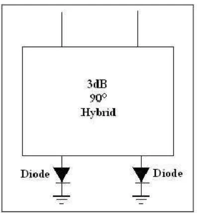
2.1.1 Hybrid Coupler Phase Shifter
The hybrid coupler phase shifter uses the fewest diodes (two per bit). The
proper design of the terminating circuit can be obtained by any phase shift increment.
This hybrid coupler provides a 3dB power split for two output arms with a 90° phase
difference. This coupler can be a branch line hybrid coupler, a backward wave or a
[image:20.595.221.419.480.694.2]proximity coupler hybrid [3].
5
2.1.2 Direct Transmission Loaded Line Phase Shifter
The direct transmission loaded line phase shifter is a method, which more
attractive for high frequency applications. The phase shifter design is based on two
factors. First factor is any symmetric pair of quarter-wavelength spaced shunt
susceptance will have mutually cancelling reflections if their normalized
susceptances are small compared with unity. The second factor is shunt capacitance
elements electrically lengthen a transmission, whereas inductive elements shorten it.
[image:21.595.146.496.295.462.2]This loaded line can be analyzed using the ABCD matrices [3]
Figure 2.2 Loaded Line Phase Shifter
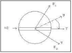
2.1.3 Switched Line Phase Shifter
This switched action to obtain insertion phase by providing alternative
transmission paths, which is the difference in electrical lengths being the desired
phase shift. This approach offers the opportunity for true time delay rather than
steady-state phase control. Although, this switched has disadvantage that the four
6
Figure 2.3 Switched Line Phase Shifter
As shown in figure, the signal flows through the lower line length of l1 if the
bias is positive. If the bias is negative, the signal flows through the lower line with a
path length of l2. The phase difference between the two bias states is [1]:
(2.3)
2.1.4 Rotary Phase Shifter
The rotary phase shifter is a precision instrument that is widely use
microwave measurements. The quarter-wave plates are oriented at an angle of 45°
relative to the broad wall of the rectangular guide in the rotary phase shifter [1].
[image:22.595.244.396.618.731.2]7
One major application of phase shifters is in phased-array antennas. Each
antenna element in phase-array antenna is connected to a phase shifter. By varying
the phase of each element, the array radiation beam can steer to the desired direction
electronically [1].
2.2 Diode
Diodes allow electricity to flow in only one direction. The arrow of the circuit
symbol shows the direction in which the current can flow. Diodes are the electrical
version of a valve and early diodes were actually called valves [3].
A little energy pushing its way through the diode is use up by electricity.
There is a small voltage across a conducting diode called forward voltage drop and it
is about 0.7V for all normal diodes which are made from silicon. The forward voltage
drop of a diode is almost constant whatever the current passing through the diode so
they have a very steep characteristic.
A perfect diode does not conduct when a reverse voltage is applied but all
real diodes leak a very tiny current of a few µA or less. This tiny current can be
ignored in most circuits because it will be very much smaller than the current
flowing in the forward direction. However, all diodes have a maximum reverse
voltage. If maximum reverse voltage is exceeded, the diode will fail and pass a large
current in the reverse direction and this is called breakdown [4].
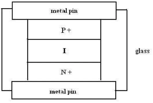
2.2.1 PIN Diode
A PIN diode is a semiconductor device that operates as a variable resistor at
RF and microwave frequencies. The resistance value of the PIN diode is determined
only by the forward biased dc current. An important additional feature of the PIN
diode is its ability to control large RF signals while using much smaller levels of dc
8
Figure 2.5 Cross Section of PIN Diode
A PIN diode obeys the standard diode equation for low frequency signals.
The diode looks like an almost perfect resistor at higher frequencies, while at low
frequencies, the charge can be removed and the diode turns off. The diode never
turns off because there is not enough time to remove the charge in high frequency.
Besides, the PIN diode has a poor reverse recovery time.
The depletion region for PIN diode exists almost completely within the
intrinsic region. This depletion region is much larger than in a PN diode and
increases the area where electron-hole pairs can be generated. The wide intrinsic
region also means the diode will have a low capacitance when reverse biased.
PIN diode is similar to the p-n diode but with a smaller junction capacitance.
The structure of PIN diode consists of a heavily doped p-region and a heavily doped
n-region separated by a layer of high resistivity material that is nearly intrinsic as
shown in Appendix A.
The device functions in forward bias or reverse biased modes. When forward
biased, injects a charge into the resistivity layer. The amount of voltage that is given
decides the amount of charge and its conductivity. This forward direction will act as