i
DESIGN AND ANALYSIS OF CMOS PIN-PHOTODIODE FOR OPTO-FLUIDIC DETECTOR
NUR YASHIDAR BINTI MOHAMAD YASIN
A thesis submitted in partial fulfillment of the requirements for the award of the degree of Bachelor of Electronic Engineering (Computer Engineering)
Faculty of Electronic and Computer Engineering
Universiti Teknikal Malaysia Melaka
ii
UNIVERSTI TEKNIKAL MALAYSIA MELAKA
FAKULTI KEJURUTERAAN ELEKTRONIK DAN KEJURUTERAAN KOMPUTER
BORANG PENGESAHAN STATUS LAPORAN PROJEK SARJANA MUDA II
Tajuk Projek : ………
Sesi
Pengajian : 1 1 / 1 2
Saya ……….. (HURUF BESAR)
mengaku membenarkan Laporan Projek Sarjana Muda ini disimpan di Perpustakaan dengan syarat-syarat kegunaan seperti berikut:
1. Laporan adalah hakmilik Universiti Teknikal Malaysia Melaka.
2. Perpustakaan dibenarkan membuat salinan untuk tujuan pengajian sahaja.
3. Perpustakaan dibenarkan membuat salinan laporan ini sebagai bahan pertukaran antara institusi pengajian tinggi.
4. Sila tandakan ( √ ) :
SULIT*
*(Mengandungi maklumat yang berdarjah keselamatan atau kepentingan Malaysia seperti yang termaktub di dalam AKTA RAHSIA RASMI 1972)
TERHAD** **(Mengandungi maklumat terhad yang telah ditentukan oleh organisasi/badan di mana penyelidikan dijalankan)
TIDAK TERHAD
Disahkan oleh:
__________________________ ___________________________________
(TANDATANGAN PENULIS) (COP DAN TANDATANGAN PENYELIA)
iii
“I declare that this thesis is the result of my own work except for quotes as cited in the references.”
Signature : ……….
iv
“I declare that I have been reading this thesis in view of our work is sufficient from the scope and quality for the award of Bachelor of Electronic Engineering (Computer
Engineering).”
Signature : ………
v
This project is gratefully dedicated to my father and mother To my beloved family
To my respected lecturer / supervisor And to all my friends
vi
ACKNOWLEDGEMENT
First and foremost, all praise to the Most Gracious and the Most Merciful Allah for giving the time and opportunity to complete my final year project and this report successfully. Without His help, none of these could be done smoothly. A deep and sincere appreciation goes to my supervisor, Mr Mohd Azlishah bin Othman, who has showered his knowledge and assisted me in completing my two semester journey by doing this research without hesitation.
Big thanks also dedicated to my second supervisor, Mr Zulatfyi Fauzan for his valuables advice during completing my research. A sincere thank you also goes to my university which is Universiti Teknikal Malaysia Melaka for giving me this chance to complete my research by giving me using lab facilities and equipments. Not to forget, thanks to my family for their encouragement, never ending support and giving in so much, either directly or indirectly, to help me complete the course.
vii
ABSTRACT
viii
ABSTRAK
ix
TABLE OF CONTENT
CHAPTER TITLE PAGE
PROJECT TITLE i
STATUS CONFIRMATION REPORT FORM ii
AUTHOR’S DECLARATION iii
SUPERVISOR’S DECLARATION iv
DEDICATION v
ACKNOWLEDGMENT vi
ABSTRACT vii
ABSTRAK viii
TABLE OF CONTENT ix
LIST OF TABLES xiii
LIST OF FIGURES xiv
LIST OF ABBREVIATIONS xviii
1 INTRODUCTION
1.1 PROJECT OVERVIEW 2
1.2 PROBLEM STATEMENT 4
1.3 OBJECTIVES 4
1.4 SCOPE OF WORKS 4
x
1.6 PROJECT OUTLINE 6
1.7 SIMULATION 6
2 LITERATURE REVIEW
2.1 PHOTODIODE 9
2.2 P+ REGION AND N+ REGION 9
2.3 I+ REGION 10
2.4 N WELL P SUBSTRATE PHOTODIODE 11
2.5 DEPLETION REGION 11
2.6 DOPING 12
2.7 PHOTO-DETECTOR 12
2.8 IV CHARACTERISTICS 13
2.9 PRINCIPLE OPERATION OF PHOTODIODE 14
2.10 REVERSE BIAS 14
2.11 GUARD RING 15
3 SILVACO TCAD AND ATLAS
3.1 TCAD 17
3.2 ATLAS 17
3.3 DECKBUILD 18
3.4 TONYPLOT 19
3.5 NEWTON METHOD 20
3.6 ATLAS OUTPUT:STRUCTURE FILES 20
3.7 ATLAS OUTPUT:LOG FILES 20
3.8 MODELS FOR BIPOLARDEVICES 21
3.8.1 Recombination 21
3.8.2 Mobility 21
xi
4 METHODOLOGY
4.1 SUMPROJECT DEVELOPMET 23
4.2 GANTT CHART
4.2.1 Gantt Chart FYP I 25
4.2.2 Gantt Chart FYP II 26 4.3 METHOD OF LITERATURE REVIEW 27 4.4 FLOW OF LITERATURE REVIEW 28
4.5 PROJECT METHODOLOGY 29
4.5.1 Stage 1 – Literature Review 29 4.5.2 Stage 2 – Design and Simulate 29 4.5.3 Stage 3 - Experimental 29 4.5.4 Stage 4 - Thesis 30
4.6 PROJECT FLOW CHART 32
4.7 CREATE STRUCTURE AND GENERATE 32 GRAPH
5 RESULT AND DISCUSSIONS
5.1 SILVACO (DESIGNS AND RESULTS) 44
5.2 DESIGNS 44
5.2.1 PIN Photodiode with Intrinsic 2mµ x 8mµ 44 5.2.2 PIN Photodiode with Intrinsic 2 mµ x
8mµ 45
5.3 RESULTS 46
5.3.1 No light or Beam Supply 46 5.3.2 With Light or Beam Supply 49 5.3.3 With and Without Light or Beam Supply 52 5.3.4 Voltage Breakdown for Different width I+ 54
xii
6 CONCLUSION AND RECOMMENDATIONS
6.1 CONCLUSIONS 58
6.2 RECOMMENDATIONS 58
xiii
LIST OF TABLES
NO TITLE PAGE
4.0 Gantt Chart PSM 1 25
xiv
LIST OF FIGURES
NO TITLE PAGE
1.0 PIN Photodiode 2
1.1a PIN photodiode operated in reverse bias, hv is the energy of 3 radiation, V is the bias, and RL is the local load resistance
1.1b IV characteristics for a pin photodiode (1) with no light (2) 3 with light
1.2 Project methodology 5
2.0 P+ Region and N+ Region 10
2.1 Intrinsic Region 11
2.2 Depletion Region 12
2.3 IV Characteristics of PIN Photodiode 13
2.4 PIN Photodiode 14
3.0 ATLAS 17
4.0 Project Development 23
4.1 Method of Literature Review 27
4.2 Literature Review 28
xv
LIST OF FIGURES
NO TITLE PAGE
4.4 Getting started with ATLAS 32
4.5 Invoking ATLAS Mesh Menu 33
4.6 ATLAS Mesh Menu 33
4.7 Mesh Values 34
4.8 Coding for Mesh Structure 34
4.9 Material 35
4.10 ATLAS Electrode 35
4.11 Electrode (Anode) 36
4.12 ATLAS Doping 36
4.13 After insert the value 37
4.14 ATLAS Save 38
4.15 Category: Mobility 39
4.16 Category: Recombination 39
4.17 Mesh Coding in DECKBUILD 40
xvi
LIST OF FIGURES
NO TITLE PAGE
4.19 Doping coding in DECKBUILD 41
4.20 Save and Beam coding in DECKBUILD 41 4.21 Model and Methods coding in DECKBUILD 42 5.0 PIN Photodiode with Intrinsic 2mµ x 8mµ (width) 44 5.1 PIN Photodiode with Intrinsic 2.4mµ x 8mµ (width) 45 5.2 Graph for Same Voltage Supply (-4V) for different i+ width 46 5.3 Graph for Same Voltage Supply (-7V) for different i+ width 47 5.4 Graph of two different voltages supply (-4V and -7V) for 48 intrinsic width 2.4mµ x 8mµ
5.5 Graph of two different voltages supply (-4V and -7V) for 48 intrinsic width 2mµ x 8mµ
xvii
LIST OF FIGURES
NO TITLE PAGE
5.9 Graph of two different voltages supply for intrinsic width 52 2 mµ x 8mµ
5.10 With and Without Light or Beam Supply for Intrinsic width 52 2.4mµ x 8mµ
5.11 With and Without Light or Beam Supply for Intrinsic width 53 2mµ x 8mµ
xviii
LIST OF ABBREVIATIONS
CMOS - Analysis of Variance
TCAD - Technology Computer-Aided Design IV - Current Voltage
RF - Radio Frequency
GUI - Graphical User Interface
EDA - Electronic Design Automation
1D - 1 Dimension
2D - 2 Dimension
Conmob - Concentration Dependent Mobility
Fldmob - Field Dependent Mobility
Auger - Auger Recombination
Bgn - Band Gap Narrowing
AC - Alternating Current
DC - Direct Current
CHAPTER 1
INTRODUCTION
2
1.1 Project Overview
[image:20.595.204.433.216.365.2]The PIN photodiode is a special case of the PN junction photodiode, in which a large intrinsic or lightly doped N semiconductor area is inserted in between the P region and N region. This is different from the PN photodiode in that the intrinsic region is much larger than that in PN diode.
Figure 1.0: PIN Photodiode [1]
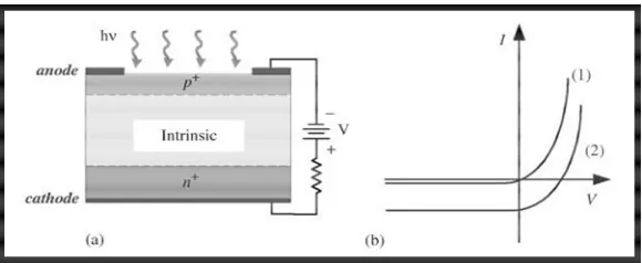
It is a well known fact that in any PN diode, the depletion region extends more into the lightly-dope N region than into the heavily doped P region. This is because, in the heavily doped region, the number of free charge carriers available for conduction is quite large compared to that in the lightly doped region [1]. In a normal operation a reverse-bias voltage is applied across the device so that no free electrons or holes exist in the intrinsic region.
3
Figure 1.1: a) PIN photodiode operated in reverse bias, hv is the energy of radiation, V is the bias, and RL is the local load resistance. b) IV characteristics for a pin photodiode (1) with no light (2) with light [2]
For enhanced performance it is often necessary for the device to have a shallow junction followed by a wide depletion region where most of the photon absorption and Electron Hole generation should take place. The magnitude of the generated current is proportional to the intensity of the incident light. It can be used as a photon detector by operating it in the third quadrant of its electrical current voltage (I-V) characteristics [3].
The PIN photodiode when forward biased by a direct current it can pass RF signals without distortion, down to some minimum frequency set by the lifetime of the carriers, holes and electrons, in the intrinsic region. As the forward current is reduced, the resistance to the flow of the RF signal is increased, but it does not vary over a half cycle of the signal frequency. As the direct current is reduced to zero, the resistance rises towards infinity, when the diode is reverse biased only a very small amount of RF current can flow, via the diode’s reverse capacitance [4].
[image:21.595.191.481.70.189.2]4
1.2 Problem Statements
In this project we target to design PIN photodiode with different size with a different sensitivity. A market survey that been done shows that there are a lot of PIN photodiode but it there have been a gap where there are a lack of PIN photodiode with less detection and sensitivity.
1.3 Objectives
The objectives of this project are to:
a) To study the theory behind PIN photodiode b) To design and analysis PIN Photodiode
c) To determine IV Characteristic of PIN Photodiode
1.4 Scope of Works
This project is based on Integrated Circuit (IC) Design which is using PIN Photodiode. This project is using SILVACO TCAD tool software to get the designs, layouts and results.
5
b) TONYPLOT is a powerful tool designed to visualize TCAD 1D and 2D structures produced by SILVACO TCAD simulators. TONYPLOT provides visualization and graphic features such as pan, zoom, views, labels and multiple plot support. TONYPLOT also provides many TCAD specific visualization functions such as HP4154 emulation, 1D cut lines from 2D structures, animation of markers to show vector flow, integration of log or 1D data files and fully customizable TCAD specific colours and styles
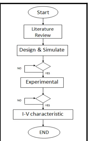
[image:23.595.262.415.304.545.2]1.5 Project Methodology
Figure 1.2: Project Methodology
In the beginning of the project, a literature review needs to be done as we want to familiar with the project. In the literature review, needs to cover up about the PIN Photodiode and SILVACO TCAD tools software so that easy to start the design of the photodiode. The schematics are then design by using DECKBUILD.
6
the results which are IV Characteristics. If the results are not satisfied with the expected one, change the coding and run it again until get the expected one.
1.6 Project Outline
Chapter I We divided our thesis into several chapters. In Chapter 1 the background research of this project were studied.
Chapter 2 examines about the literature review of this project on designing PIN Photodiode and its performance characteristic which is IV Characteristics.
Chapter 3 Explain about SILVACO TCAD and ATLAS
Chapter 4 summarizes the methodology of this project. In this chapter, we explain how the project has been done.
Chapter 5 presents the results and explain about the discussions of IV Characteristics of the PIN Photodiode by using SILVACO TCAD tools software. The discussion is about the finding and observation from the layout design.
Chapter 6 clarifies the conclusion and some improvement for this project. The improvement of this project is clearly explained in this chapter.
![Figure 1.0: PIN Photodiode [1]](https://thumb-ap.123doks.com/thumbv2/123dok/570577.67493/20.595.204.433.216.365/figure-pin-photodiode.webp)