THE INSTITUTE OF ELECTRONICS, IEICE ICDV 2012 INFORMATION AND COMMUNICATION ENGINEERS
Copyright ©2012 by IEICE
An Investigation on I-V Characteristic for CMOS PIN Photodiode:
Variable I-Layer
M.A.Othman, Z.A.F.M.Napiah, N.Y.M.Yasin, T.S.M.Arshad, M.M.Ismail,
H.A.Sulaiman, M.H.Misran, M.A.M.Said
Centre for Telecommunication Research and Innovation
Fakulti Kej. Elektronik dan Kej. Komputer
Universiti Teknikal Malaysia Melaka
76100 Durian Tunggal, Melaka, Malaysia
[email protected], [email protected], [email protected],
[email protected], [email protected],
[email protected], [email protected], [email protected]
Abstract - In this paper presented an investigation on I-V characteristic for CMOS PIN Photodiode. PIN diodes are
widely used in optics and microwave circuits as it acts as a current controlled resistor at these frequencies. PIN diode
performance is greatly influenced by the geometrical size of the device, especially in the intrinsic region. Two different
I-layer thickness of PIN diode structure has been designed using Sentaurus Technology Computer Aided Design
(TCAD) tools. The I-layer thickness (or width) is varied from 4 µm to 8 µm in order to investigate its effects on the
current-voltage (I-V) characteristics. These structures were design based on CMOS process.
Keyword - PIN Photodiode, Silvaco TCAD, IV Characteristic, Reverse Bias
1.
Introduction
Nowadays a lot of microwave and optical devices have been design by academician, scientist and engineers. One of two terminal devices that get intention is PIN diode. PIN diodes name attribute to overall their structure where P is P type layer, I intrinsic layer and N is N type layer. The intrinsic layer is interesting layer since this layer makes the PIN diodes application comes to be as attenuators, RF switches and photodiode. Hence, PIN diodes are used extremely in RF and microwave applications due to ability to control the magnitude and phase of the signals [1], [2]. In addition, the ability to control RF and microwave signals while using a smaller level of dc excitation makes the PIN diode suitable for attenuating, limiting, phase shifting, modulating an d microwave switching.
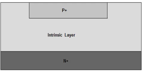
The I-layer or intrinsic layer is the one that gives a changes in-term of properties comparing with PN diode. The intrinsic layer comprises of undoped or virtually undoped semiconductor and in most PIN diodes and very thin between 1 µ m up to 200 µ m. PIN photodiode is a special case of the PN junction photodiode, in which a large intrinsic or lightly doped N semiconductor area is inserted in between the P and N region as shown in Figure 1 below.
Figure 1: PIN photodiode structure.
It is a well-known fact that in any PN diode, the depletion region extends more into the lightly-dope N region than into the heavily doped P region. This is because, in the heavily doped region, the number of free charge carriers available for conduction is quite large compared to that in the lightly doped region [3 ]. In a normal operation a reverse -bias voltage is applied across the device so that no free electrons or holes exist in the intrinsic region.
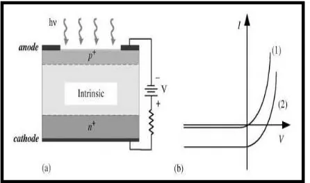
Figure 2 (a) PIN photodiode operated in reverse bias, h v is the energy of radiation, V is the bias, and RL is the local load resistance (b) IV characteristics for a pin photodiode (1) with no light (2) with light.
In a generic photodiode, light enters the devise through a thin layer whose absorption typically causes the light intensity to exponentially drop with penetration depth. For enhanced performance it is often necessary for the device electrical current voltage (I-V) characteristics.
PIN photodiode is usually functioning by appl ying a reverse-bias voltage. The magnitude of the reverse -bias voltage depends on the photodiode purpose, but naturally is less than a few volts. While no light is incident on the photodiode, a current is still produce [5].The objectives of this paper are to stud y the theory behind PIN photodiode , to design and anal yze PIN-Photodiode and to determine characteristic of PIN -Photodiode.
2.
Design and Simulation
The simulations were performed using Silvaco ATLAS. Silvaco ATLAS is a TCAD product which is ph ysics based on modeling system. This allows TCAD to predict device performance based upon equations which describe the physics within the structure of the device [6].
The structure under consideration of lightly doped with 5.e16 for N-epi doping, 1e20 for N+ doping, 1e20 for P+ doping, sandwiched with I+ doping with concentration 1e21. The incident light absorbed in neutral P+ region and neutral N+ region as well as in the depleted N - region.
All the calculations presented in this work have been obtained with ATLAS software of SILVACO unless stated
otherwise. The intrinsic region size had been varied with 2 different sizes which is 4µ m and 8µ m in width.
ATLAS enables device technology engineers to simulate the electrical, optical, and thermal behavior of semiconductor devices. Di fferent models such as conmob, fldmob, srh, auger and bgn are used for effective implementation of changes occurri ng related to radiation damage [7].
3.
Results and Discussion
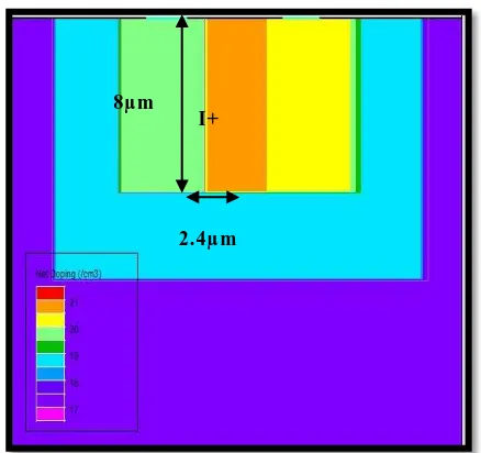
Intrinsic region width of the device was varied and the effect on device characteristics was analyzed. Figure 3 and figure 4 shows the differences size of intrinsic region. Electrons are also produces photon absorption in the p (n) regions, but the component of photocurrent due to these effects tends to distort the photo detector response.
This is because the minority carriers in the p and n regions diffuse slowly into the depletion region, resulting in a delayed response compared with the dominant, depletion region drift response. By increasing the width of depletion region, which is intrinsic region can solves these problems. Thereby, it will cause larger fraction of the light/beam to fall on the depletion region [6].
As shown in the figure, the intrinsic width for both structures had been increased to 0.4 µ m. By capturing most of the light in the depletion region (intrinsic la yer), it will effect to improve the responsivity of the device. To fully benefit from the intrinsic layer or deplet ion region, the PIN Photodiode normally requires an applied reverse bias that ensures a depletion region extension all the way through this layer.
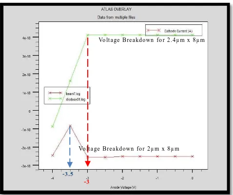
Figure 5, 6 and 7 shows the simulated I-V characteristic of Silicon PIN Ph otodiode for the structure that ha d been created. The simulated results of p+, i+, n+ photo detector are obtained by developing a program in DECKBUILD window, interfaced with ATLAS, simulation software of SILVACO and TonyPlot.
Figure 6 show the difference of IV characteristic when supply light and without supply light for 2µ m x 8µ m. Basically, it use the same theory with the result show in figure 5, the difference is the size of depletion use based on the structure. For IV Characteristic in figure 5, it uses huge depletion size compared to IV Characteristics in figure 6. That is why the effect of shifting of IV Characteristics from the photodiode is smaller compared to IV Characteristic in figure 5 due to difference structure used.
Based on figure 7, it shows the voltage b reakdown for 2µ m x 8µ m and 2.4µ m x 8µ m. There is a difference for the voltage breakdown between each structure. Voltage breakdown for intrinsic for 2.4µ m x 8µ m is faster compared to Voltage breakdown for intrinsic for 2µ m x 8µ m. This is due to the depletion region in the structure since the size of intrinsic is not the s ame.
Based on graph in figure 5 and figure 6, the shape of graph had a little bit difference in their variance. This is due to the size of the mesh that had been varied since the size of intrinsic layer had been changed. Thus, the mesh for Intrinsic with 2µ m x 8µ m becomes closer and that is why variance appeared.
Figure 3: Intrinsic with 2µ m x 8µ m
Figure 4: Intrinsic with 2.4µ m x 8µ m
Figure 5: Intrinsic with 2.4µ m x 8µ m
Figure 6: Intrinsic with 2µ m x 8µ m 8µm
2µm I+
8µm
2.4µm I+
With ligh t With o u t lig h t
4 . 1 2 5e - 1 8
0 .7 5 e -1 8
1 e-1 8
-1 .1 2 5 e -1 8
Figure 7: Voltage Breakdown for 2µ m x 8µ m and 2.4µ m x 8µ m
4.
Conclusion
In this study, in order to observe the width of intrinsic or depletion region effect on the IV Characteristics performance, the two-dimensional silicon PIN photodiode with varying width has been simulated using the SILVACO TCAD tools. Through the simulations, it shows that there is a difference occurs during voltage breakdown for difference intrinsic size. PIN Photodiode give effect when light supplied to the photodiode by shifting the IV Characteristics down. In general, PIN photodiode need small voltage supply to have a better I-V performance (voltage breakdown) .
5.
Acknowledgement
Authors would like to thank Centre for Telecommunication, Research and Innovation (CeTRi), Universiti Teknikal Malaysia Melaka for their equipment, assistance support and also financing the conference’s paper .
References
[1] Yashchyshyn, Y., "Reconfigurable Antennas b y RF Switches Technology", 5Ih International Conference on Perspective Technologies and Met hods in MEMS Design, pp. 155 -157, April 2009.
[2] Yang, J. G., Kim, M., Yang, K., "An InGaAs PIN-diode based Broadband Travelling -wave Switch with High -Isolation Characteristics, " IEEE International Conference on Indium Phosphide and Related Materials, pp. 207-209, May 2009.
[3] B. Somanathan Nair, Electronic Devices and Applications, 3rd Edition, pp. 330, September 2006. [4] G. Keiser, “Optical communications essentials,”
McGraw-Hill, pp. 108, 2003.
[5] J. Piprek, “Optoelectronic Devices: Advanced Simulation And Analysis,” Springer Media and Business, pp. 382, 2005.
[6] C.K. Maiti, G.A. Armstrong, “TCAD for Si, SiGe and GaAs Integrated Circuits,” The Institute of Engineering and Technology, pp. 47, 2007.
[7] D. Vasileska, S.M. Goodnick, “Computational Electronics,” Morgan and Cla ypool Publishers, pp. 98, 2006.
Vo lt a ge B re a kd o wn fo r 2 µ m x 8 µ m Vo lt a ge Bre a kd o wn fo r 2 . 4 µ m x 8 µ m
-3 .5