THE INSTITUTE OF ELECTRONICS, IEICE ICDV 2012 INFORMATION AND COMMUNICATION ENGINEERS
Copyright ©2012 by IEICE
I-V Characteristic at Different Depletion Region for CMOS PN Photodiode for
Optical Communication Applications
[email protected], [email protected], [email protected], [email protected], [email protected],
[email protected], [email protected], [email protected]
understanding of IV characteristic will be presents in this paper.
Keyword - PN photodiode, IV Characteristic, Silvaco TCAD
1.
Introduction
heart of the most photocells, rectifiers and transistors. It is also cheaper and has greater sensitivity [1].PN junction forms a diode, and consequently a structure of PN photodiode is simulated with different size of P+ region and the analysis of I-V characteristic which is use Silvaco TCAD tools discussed in the next topic.
Figure 1: PN Junction Photodiode [3]
1.2.
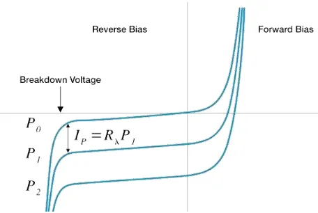
Reverse Biased
The PN junction operated in the reverse biased condition. The PN photodiode operation involving light and the light will be directed fall on the upper top of the photocurrent [4]. When a reverse bias voltage is applied to the PN junction, more electrons and holes are attracted to the contact. As a result, more donor and acceptor ions appear at the depletion region which in turn increases as well. [5].
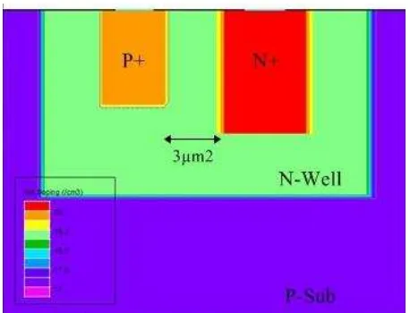
Figure 6: PN Photodiode with width, W= 3 µ m2.
Figure 7: IV curve for PN Photodiode with width, W= 3 µ m2.
Figure 8: I-V curve of PN Photodiode with different width.
In reverse bias, the number of free carriers in the device depends primarily on the current in the device and the voltage is clamped at the knee voltage of the diode. Because of the IV curve for the photodiode in reverse bias is exponential, a small change in V has a much larger impact to the device.
3.2.
Presence of light
For the analysis of presence of light, the second structure is chose, shown in Figure 6. From the analysis, some photon are incident on the surface of PN photodiode. Since the photon will pass through it and strike the junction. Light that is absorbed by the photodiode produces current flow through the entire external circuit.
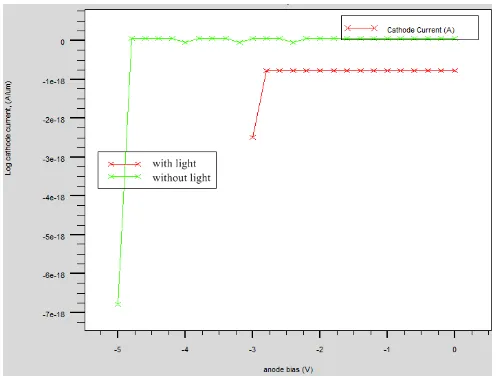
The depth at which the photons reach into the depletion region depends on the incident of light. Figure 9 show the IV curve with no light falling on the PN photodiode. When no light is falling on the photodiode, a very small current passes through the photodiode. This cu rrent is basically due to the reverse bias applied to the PN photodiode.
Figure 10 show the IV curve with light falling on the P N photodiode. As the light is incident on the photodiode, photocurrent is developed. This photocurrent gets increased by increasing the light intensity.
Figure 10: IV curve for PN Photodiode with light.
Figure 11: I-V Curve of PN Photodiode with presence of light.
4.
Conclusion
In this paper, the different width of depletion region effects of the PN photodiode on its I-V characteristics has been successfully simulated and verified. The presence of light also affects the IV curve of the PN photodiode. In order to perform the I-V curve, the SILVACO TCAD is used. The result is compared between the different of structure. It is proved that the smaller width of depletion region, the better the device. From this paper also can conclude that the photocurrent gets increased by increasing the light intensity.
5.
Acknowledgement
The authors would like to thanks Universiti Teknikal Malaysia Melaka, Malaysia (UTeM) for their equipment, financial and assistance support . Last but not list, the author would like to thanks those involved direct and indirect in completing this project success fully.
References
[1] C. Y. -T. Chiang and Y. T. Yeow, "Inverse Modelling of Two-Dimensional MOSFET Dopant Profile via Capacitance of the Source/Drain Gated Diode ," IEEE Transaction on Electron Devices, vol. 47, no.7, pp. 1385-1392, 2000.
[2] S.B. Alexander, “Optical Communication Receiver Design,” SPIE Press, 1997.
[3] B.S. Nair, “Electronic Devices and Application ,” Prentice-Hall India, pp. 329, 2006.
[4] F. Chou, C. Wang, G.Chen, Y.sin, “An 8.7 GHz Si photodiode in standard 0.18 -μm CMOS technology,”OECC, pp. 826-827, 2010.
[5] Mohamad, M., Jubadi, W.M., Tugiman, R., Zinal, N.,
Zin, R.M. “Comparison on I-V performances of
Silicon PIN diode towards width variations,” IEEE ICSE, pp. 12-14, 2010.
[6] Silvaco, “Atlas User’s Manual: Device Simulation
Software,” Silvaco International, 2000.
![Figure 1: PN Junction Photodiode [3]](https://thumb-ap.123doks.com/thumbv2/123dok/571084.67574/1.595.75.266.645.740/figure-pn-junction-photodiode.webp)