Practical Design Strategy for Two-phase Step up
DC-DC Fibonacci Switched-Capacitor Converter
Yan Chiew Wong, Wei Zhou, Ahmed O. El-Rayis, Nakul Haridas, Ahmet T. Erdogan, Tughrul Arslan
Advanced Smart Antenna Technologies Research Group, School of Engineering, University of Edinburgh, EH9 3JL, UK {Y.Wong, W.Zhou, A.El-Rayis, N.Haridas, Ahmet.Erdogan, T.Arslan}@ed.ac.uk
Abstract—The Fibonacci Switched-Capacitor (SC) converter demonstrates the highest performance by using minimum number of capacitors. However, as the Fibonacci SC requires a wide range of voltage rating of the devices, its implementation is difficult. This paper presents two gate driving techniques for designing and implementing two-phase Fibonacci SC converter for both low and high step-up conversion ratios. The proposed gate driving techniques only require few auxiliary transistors to provide the required boosted voltages for turning the charge transfer switches in the converter on and off. As a result, the proposed gate driving techniques reduce the design complexity and increase the reliability of the Fibonacci SC converter. Practical 8X and 5X Fibonacci SC converters are simulated and constructed based on the proposed techniques. The high conversion efficiencies achieved prove the effectiveness of the proposed techniques.
I. INTRODUCTION
A DC-DC SC converter is an inductorless converter that uses only capacitors and switches without involving amplifiers or transformers to step up or step down the voltage. This approach has the advantages of simple control method, reduced physical volume, less electromagnetic interference (EMI), low cost and high power density for its design. Among various types of SCs, 2-phase SC appears as one of the most promising topologies due to its simpler switching circuitry when used in mobile devices. Fibonacci topology shows another advantage, by using the minimum number of capacitors for the highest conversion ratio compared to Dickson and voltage doubler topologies. Capacitors consume considerable silicon area in integrated circuit (IC) implementations, thus by reducing the number of capacitors, a smaller size integrated converter can be obtained.
Extensive studies of SCs have been performed, but most of these treat switches as ideal components [1-3]. Analytical ideal models of Fibonacci SC converters have been well characterized to achieve a range of distinct DC conversion ratios [1, 3]. However, these works are based on pure topology aspects which exclude the considerations of capacitance values, charge transfer switches components and gate control techniques. In [4-6], some gate control methods for Fibonacci
converters were proposed for low to medium conversion ratios but with the expense of having more switching phases. Better understanding of various issues relating to practical implementation of SC converters is essential in order not to exceed the technology limits of the components used in the implementation.
In Section II, the characteristics of transistors as charge transfer switches are presented. The implementation strategy of the transistors for the Fibonacci SC topology is discussed in Section III. The SC converter is optimized based on its capacitors and switches in Section IV. Finally, the SC converter is simulated and realized with discrete components based on the proposed design strategy in Section V and conclusions are provided in Section VI.
II. CHARGE TRANSFER SWITCHES COMPONENTS
The Fibonacci topology is based on an N-stage SC converter with the final voltage ratio limited by (N+1)th Fibonacci number (F(N+1) ) [1-3, 5]. This conversion ratio is
the highest ratio that can be attained from a 2-phase SC converter by using N-1 capacitors. Theoretically, the conversion ratio can be ranged from 1, 2, 3, 5, 8, 13, 21, and so on. However, the implementation of the Fibonacci SC converter is limited by the transistor technology employed [7]. For SC converter implementation, MOSFETs have to be designed to operate in linear region to transfer a high current with a small on-resistance [5, 6]. Both n-channel MOSFET (nMOS) and p-channel MOSFET (pMOS) transistors have their difficulties in switching on and off. Completely switching on and off of MOSFETs is the key in developing an energy efficiency converter. An nMOS transistor can be easily switched off by applying a gate voltage of 0V or effective gate to source voltage (VGS_eff) smaller than the VTH [6, 8].
However, to switch on the nMOS without suffering from a significant voltage drop, the VGS_eff of the nMOS has to be
higher than the boosted voltage at the subsequent higher stages after deducting the VTH [6, 9]. The VTH increases when a
bulk potential (VB) is applied [8]. This increases the body
effect of the transistor which leads to deteriorating the performance of an nMOS transistor as a charge transfer switch. The body effect is minimized in low conversion ratio DC-DC converters where the bulk of nMOS is grounded and VB is zero potential. However, for a higher conversion ratio, if
VB is still with zero potential, it may cause the transistor to
The authors would like to thank the SOFANT for their support in this work.The authors gratefully acknowledge the financial support from the Universiti Teknikal Malaysia Melaka and Malaysia Government.
2011 20th European Conference on Circuit Theory and Design (ECCTD)
break down when the potential between drain/source/gate terminal (VD/S/G)and VB is greater than a technology specific
voltage limit. Thus, for higher conversion ratio designs, the bulk of an nMOS transistor is connected to the lower terminal between drain and source [10]. However, increasing drain and source voltages in subsequent stages will increase the VB.
Thus, the converter will suffer from the body effect with a higher VTH induced by VB [8, 11]. The transconductance
between source and bulk (gs) as shown in (1) can no longer be
ignored. As the number of convertor stages increases, the overall VTH increases as well, and this decreases the voltage
gain per stage. Eventually, this body effect seriously diminishes the DC-DC converter output voltage.
p n si
eff GS pi n p OXn p n F TH
TH
L g
V W C V
V
/ _ / / / 2
0
2 |
2 |
µ γ φ
γ +
−
= (1)
where VTH0n/pis the threshold voltage with zero VSB of nMOS or pMOS, gs is
the transconductance between source and bulk, VGS_eff =VGS_CLK-αNVTH0n/p,
VGS_CLKis switching clock’s amplitude, αis the coefficient proportional to
the number of charge pump’s stages with the values between 0<α<1 and N is the number of stages of charge pump
As for pMOS based SC converters, pMOS transistors can be easily switched on by setting VGS_eff ≤ 0V. However, it is
difficult to completely switching off the pMOS switches. To avoid leakage currents from drain/source to substrate, the bulk of pMOS transistors should be connected to the highest terminal [6, 9, 11, 12]. In the next section, an effective gate driving technique will be introduced in order to minimize the effects of the transistors. Auxiliary transistors will be used to generate boosted pump clock schemes to ensure the transistors are always fully switched on and off.
III. TRANSISTOR GATE DRIVINGTECHNIQUE
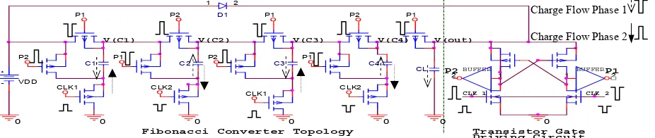
Effectively driving the gate of the transistors is essential to ensure that the transistors work in linear or cut-off region while being switched on and off, respectively. As shown in Fig. 1, when clock 1 (CLK1) is HIGH, a boosted signal is obtained at output port P2 which follows CLK1, but has a higher magnitude. Similarly, P1 follows CLK2 which is non-overlapped version of CLK1. These boosted signals (P1 and P2) are used to trigger the transistors to switch on or off, to form the alternating charges flow across the capacitors for phase 1 and phase 2, as shown in Fig. 1. By connecting the source and bulk of the pMOS transistors to the highest terminal of each stage, this can effectively reduce the leakage current to substrate. Since pMOS transistors provide high efficiency in charge transferring, in our design most of the switches are pMOS based. nMOS transistors are used for the switches located near the ground terminal, as shown in Fig. 1. When the bulk terminals of the nMOS transistors are connected to the ground terminal, the body effect of the nMOS transistors can be eliminated which can lead to increasing the overall voltage gain per stage.
For a low input voltage supply (VDD), e.g. 1V to 2V, the
output voltage (Vout) of the Fibonacci topology is fed to the
level shifter for boosting the magnitude of the switching voltage. A diode is placed between VDD and the level shifter to
provide an initial voltage for starting up the level shifter. When the output voltage is higher than VDD, the diode will be
turned off. By swinging P1 and P2 voltages between 0V and
F(N+1)*VDD, a sufficient voltage level can be obtained for
switching off the pMOS transistors. To switch on the nMOS transistors, a voltage of VDD is enough when the source and
bulk terminals of nMOS transistors are connected to the ground. Both pMOS and nMOS transistors can be easily switched on and off by using 0V respectively. This low voltage gate control technique is quite straightforward, since these transistors will not face the risk of exceeding their technology maximum gate source voltage (VGS_MAX) and drain
source voltage (VDS_MAX) limits. High voltage thick oxide
transistors can be used with this topology to avoid transistor gate oxide breakdown, if a higher output voltage is required.
For the Fibonacci converter supplied with a high VDD, e.g.
3V to 5V, a different approach has to be used. By using a similar method to the one shown Fig. 1, the transistors might suffer from gate oxide breakdown due to exceeding their transistors technology limit. For high conversion, auxiliary transistors have to be used to boost the voltage at each stage or cell based on the reference voltage on other nodes. As shown in Fig. 2, each cell of the converter consists of three main charge transfer switches. Each switch has to able to be turned on and off at the designated clock phases to allow the charge to be pushed to the next stage, and block the charge from leaking to previous stage or ground. This approach is different from the linear topology such as the Dickson converter. In the linear topology, CLK1 and CLK2 are able to access each cell node, thus an initial voltage can be pumped through the capacitors in parallel. A backward control which uses the already established high voltage to control the transistors of the previous stage is applied in the linear topology [11]. This approach is not suitable for the Fibonacci converter, where clock phases are not directly attached to the capacitors. In the Fibonacci converter, all capacitors are flying capacitors, which mean both end terminals of the capacitors are connected with switches rather than fixed at supply/ground terminal, as shown in Fig. 2. In this paper, we propose a forward control technique for the Fibonacci converter. By using the previous cell node voltage, e.g. V(C2), as the source voltage and the
current cell voltage, V(C4), as the drain voltage for auxiliary
inverters, the charge transfer switch, MP1_4, can be turned on by V(C2) and turned off by V(C4), as shown in Fig. 2. For the gate drive of transistor MP1_4, it is not appropriate to control the gate voltage of transistors by switching them between 0V and F(n+1)*VDD, as presented in [6] for the Fibonacci converter
with a high power supply. The gate of the transistor will suffer from breakdown with the high voltage level stresses at VGS.
For instance, a VGS voltage of – 29.6V needs to be held by the
transistor in an 8X Fibonacci converter with a 3.7V of VDD. For
the middle transistor, MP2, a gate drive circuit is also needed to generate a boosted voltage for switching MP2 on and off at the designated clock phases. Therefore, the drain of MP2 is connected to the drain of MN1 while the source port of MN1 is grounded. For the high power supply Fibonacci converter, the voltage at the drain of MN1in the higher stages will sustain some voltage levels rather than being grounded, due to an increasing volume of charge trapped in the capacitors. Therefore, for long cascaded stages of the Fibonacci converter, there will be a voltage present at V(C4_0), as shown in Fig. 2. It is easier to switch on and off MN2 by using an inverter. MN2 can be turned on by V(C4) and turned off by V(C4_0). By using the reference voltage for switching the
V(out)
Figure 1. The 8X Fibonacci SC converter with effective gate driving technique for a low voltage supply
P1
Figure 2. Effective gate driving technique for long cascaded high voltage supply Fibonacci converter
transistors, it will not exceed the technological limits of VDS_MAX and VGS_MAX of the transistors. For the bottom nMOS
transistor, MN1, with its ground reference terminal, a voltage level of 0V and VDD is enough to turn the transistor off and
on.
For the long cascaded stages of the Fibonacci converter, a level shifter can be used to provide the required voltage levels for the transistors at the first, second and third cells, as shown in Fig. 2. For the fourth and higher stages of cells, the forward control technique can be used, for effectively driving the transistors. The voltage supply (VLS) of the level shifter has to
be connected to the internal cell node rather than the output voltage of the converter in order to avoid the breakdown of the transistors. By doing this, the number of auxiliary transistors can be reduced and the transistors remain operating within the specification margins.
IV. OPTIMIZATION OF THE FIBONACCI TOPOLOGY
The Fibonacci topology can be optimized based on capacitors or charge transfer switches. By optimizing these two elements, slow and fast switching limits of a converter can be determined. Capacitors in the Fibonacci converter do not carry the same DC voltages. Capacitor voltages in a given Fibonacci converter follow the Fibonacci sequence [3]. By using the charge balance model (2), the size of the charge storage capacitor (CStore) should be arranged in reverse order
of the Fibonnaci sequence, as shown in Fig. 3. The largest capacitor should be placed next to VDD and the smallest next
to CL. For the implementation of the Fibonacci topology,
ceramic capacitors, which have a low equivalent series resistance (ESR), are the candidate of choice either for
converters in IC form or implemented through discrete components.
V Q C= /
(2)
The optimization can also target the sizes of charge transfer switches. Using too large switches will increase the parasitic loss; conversely, smaller sized switches are not able to accommodate sufficient amount of charge, which results to a lower output voltage for a particular frequency. Sizes of the charge transfer switches should follow the multiplier (q), as shown in Fig. 3.
Figure 3. Charge flow and optimization in Fibonacci topology
V. SIMULATION RESULTS
To demonstrate the effectiveness of the proposed gate driving techniques for the Fibonacci SC converter, a cascaded high supply voltage SC converter, as shown in Fig. 3, is designed and simulated using the AMS 0.35 mµ
technology. A VDD of 3.7V was supplied to the converter.
The widths and lengths of the transistor were set to 1000 mµ
and 1 mµ respectively. CStore was set to the market available
size, 33nF. Non-overlapping clock signals, CLK1 and CLK2, were generated for switching the converter to avoid charge leakage from short circuit path. A high voltage transistor device model VGS_MAX and VDS_MAX of 20V was chosen for the
simulation of this converter.
Charge Flow Phase 1
Charge Flow Phase 2
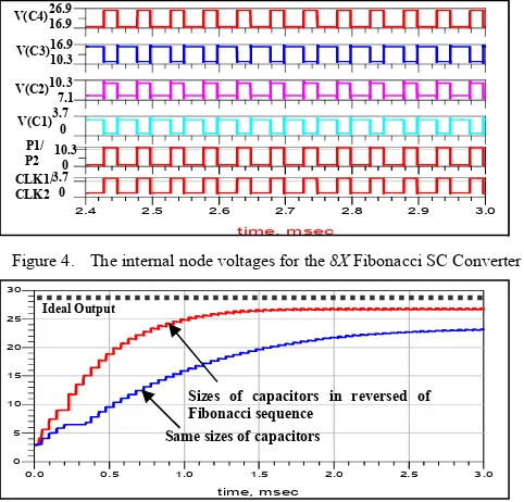
The results obtained demonstrate the effectiveness of the proposed gate driving techniques for the Fibonacci SC converter, providing a conversion efficiency, η, of up to 88%. The switches can be turned on and off at the designated clock phases and without exceeding their transistor technology limits, as shown in Fig. 4. The magnitudes of CLK1 and CLK2 swing from 0V to 3.7V, while the magnitudes of P1 and P2 swing from 0V to 10.3V. Both switching signals remain within the VGS_MAX of the transistors. Similarly, VDS_MAX of the
transistors is kept within the transistor technology limits. For example, VDS of MP1_2 is determined by the voltage
difference between V(C1) and V(C2) which is less than 20V. Slow and fast switching limits of the converter are also demonstrated. A faster rise-up time can be obtained by multiplying the capacitors with the reverse of the Fibonacci sequence. Whereas, using same size capacitors will lead to an output with a longer rise-up time, as shown in Fig. 5.
16 28
..
.
V
9 18
..
.
V
6 11
..
.
V
3 8
..
.
V
-1.0 9.5
..
.
V
2.5 2.6 2.7 2.8 2.9
2.4 3.0
-1 3
time, msec
..
.
V
Figure 4. The internal node voltages for the 8X Fibonacci SC Converter
0.5 1.0 1.5 2.0 2.5
0.0 3.0
5 10 15 20 25
0 30
time, msec
Figure 5. The output voltages for the 8X Fibonacci SC Converter
Although the design is intended for an integrated circuit implementation, it can also be realized by using discrete components, as shown in Fig. 6. A function generator was used to generate the input non-overlapped clock signals CLK1 & CLK2. Fig. 6 and Fig. 7 show the 5X Fibonacci SC converter assembled by using discrete components which provides a conversion efficiency η of 72%. The slightly lower efficiency is due to the higher VTH and on-resistance when
discrete components are used.
Figure 6. A 5X Fibonacci SC converter assembled by discrete components
Figure 7. The measurement result of the fabricated converter
VI. CONCLUSIONS
A novel design strategy for the two-phase Fibonacci SC converter has been presented. Two gate driving techniques have been proposed for effectively turning on and off the switches. In addition, the proposed Fibonacci SC converter topology has been optimized for its switches and capacitors. Simulation results obtained showed the effectiveness of the proposed design strategy.
REFERENCES
[1] M. S. Makowski, "On performance limits of switched-capacitor multi-phase charge pump circuits. Remarks on papers of Starzyk et al," in International Conference on Signals and Electronic Systems, 2008. ICSES '08. , 2008, pp. 309-312.
[2] K. Chi-Wah, et al., "Design strategy for two-phase switched capacitor step-up charge pump," in IEEE International Conference of Electron Devices and Solid-State Circuits, EDSSC 2009., 2009, pp. 423-428. [3] M. S. Makowski, "Realizability conditions and bounds on synthesis of
switched-capacitor DC-DC voltage multiplier circuits," IEEE Transactions on Circuits and Systems I: Fundamental Theory and Applications, vol. 44, pp. 684-691, 1997.
[4] Y. Hairong and C. Zhiliang, "A two-phase, four and five boosting ratio, charge pump cell for LCD driver," in 4th International Conference on ASIC, 2001, 2001, pp. 266-270.
[5] L. Lifang and C. Zhiliang, "Analysis and design of Makowski charge-pump cell," in 6th International Conference On ASIC, 2005. ASICON 2005. , 2005, pp. 497-502.
[6] W. Oi-Ying, et al., "A novel gate boosting circuit for 2-phase high voltage CMOS charge pump," in IEEE International Conference of Electron Devices and Solid-State Circuits, 2009. EDSSC 2009. , 2009, pp. 250-253.
[7] M. D. Seeman and S. R. Sanders, "Analysis and Optimization of Switched-Capacitor DC-DC Converters," IEEE Transactions on Power Electronics, vol. 23, pp. 841-851, 2008.
[8] K. M. David A. Johns, Analog Integrated Circuit Design: John Wiley & Sons, Inc., 1997.
[9] S. Feng, et al., "Gate control strategies for high efficiency charge pumps," in IEEE International Symposium on Circuits and Systems, 2005. ISCAS 2005. , 2005, pp. 1907-1910 Vol. 2.
[10] R. Pelliconi, et al., "Power efficient charge pump in deep submicron standard CMOS technology," IEEE Journal of Solid-State Circuits, vol. 38, pp. 1068-1071, 2003.
[11] W. Jieh-Tsorng and C. Kuen-Long, "MOS charge pumps for low-voltage operation," Solid-State Circuits, IEEE Journal of, vol. 33, pp. 592-597, 1998.
[12] C. Jeongwon, et al., "Analysis and Design Techniques of CMOS Charge-Pump-Based Radio-Frequency Antenna-Switch Controllers," IEEE Transactions on Circuits and Systems I: Regular Papers, vol. 56, pp. 1053-1062, 2009.
Level Shifter Buffer for P1& P2 Same sizes of capacitors
Sizes of capacitors in reversed of Fibonacci sequence
Ideal Output CLK1/ CLK2
P1/ P2 V(C1) V(C2) V(C3) V(C4)
16.9 10.3
10.3 7.1
3.7 0 3.7 0 26.9 16.9
10.3 0
14 V 9 V
6 V 3V 0V 3.7V
0V
CLK1 & CLK2 Generator
The Fibonacci Converter