S
ntre for Telec ering, Univers
cal & Electron
act—This pap
ouble Throw nications. A c
p to allpass r d. In this ana nce and atten e shunt PIN
ireless data co s commonly u
, the SPDT sw up-converter o
N diodes or F communicatio of the key par iver port. How
GHz) if using SOT23, SOT32
Fi
e are two mos shunt or com ption of the cir inductance val ntly, there is in [10] and [1 g elements (PI d in [11], to
hable
on Im
N. A. S communication siti Teknikal M
2 nuation pole i
diode with s ained with th ble radial stu requency of 3 al applicatio m.
ch, SPDT, res
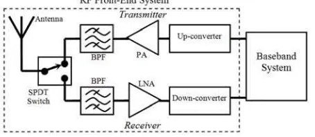
ommunication used in RF fro witch is part o or down-conv FETs where di on or base stat rameters in SP wever, it is di g single low p
23, SOD323 o
g. 1. Application
st popular tech mbination of se rcuit. Second,
lues.
a technique 1]. The key a IN diode or FE
cater for wire
Radi
mprov
Shairi #1, B. H n Research & Malaysia Mela s switchable screte switch ed discrete PI ere an analyt ation between
s determined switchable ra he switchable ub resonator 3.5 GHz givin on of this S sonator, radia I. ns using Time ont-end system
of other subco erter) [6]. Un iscrete PIN dio tion applicatio PDT switch d ifficult to get performance P or SOD523.
of SPDT switch
hniques to incr eries-shunt [8] the parallel re using switcha dvantage of th ET) compared eless broadban
ial Stu
emen
H. Ahmad #2, & Innovation (Caka (UTeM), H Malaysia. azwan@utem.
thor: badrulhi nt, Universiti T
ronoh, Perak, ngwen@petro radial stub r h for Time D IN diode is u tical modelin n inner radia d. Isolation im
adial stub re e radial stub
has shown ng better iso SPDT switch
al stub, switc INTRODUCTI e Division Du m [1] to switc
omponents su ntil now, the odes are still ons [7]. design is the re
isolation of S PIN diodes. T
in RF front-end
rease isolation ]. However, u esonant of ind able resonato his technique d to the techni and application
ub Re
t of S
, Peng Wen W CeTRI), Facul Hang Tuah Jayedu.my used to switch
g of the swit al and angle r mprovement i esonator whe b resonator. I more than 3 lation compa h is TDD sw chable resona
ION
uplex (TDD), h between tra uch as antenna switching ele desirable for h equirement o SPDT switch The PIN diode
system for wirele
n. First, multi using multiple ductor with PIN or for isolation
is reduction o ique using mu n, wider isola
esonat
PDT
Wong *3lty of Electron ya, 76100 Dur
edu.my ronas (UTP),
r isolation im plex (TDD) s h the radial st
chable reson radial stub w is analyzed w ere it is foun In measurem 30 dB of tran ared to conve witching for ator
Single Pole D ansmitter and
a [2]-[3], filter ements in the higher power
f high isolati higher than 2 es are usually
ess communicatio
ples connectio s PIN diodes, N diode [9]; b n improveme f circuit size w ultiples connec
ation bandwid
tor for
Switc
nics and Comp urian Tunggal,
Bandar Seri I
mprovement switching of tub resonator nator is prese with the char with two-port nd that an a ment result, t nsmit-receive entional SPD r WiMAX a
Double Throw receiver. As er [4], amplifie
SPDT switch levels used in ion between tr 20 dB (for ap y in standard p
ons.
on of PIN dio , it will increa but it has a lim f wireless r between n military,
ransmitter pplications packaging
odes either ase current mitation of switch as m usage of
widening open stub series cap In ord good can quarter w dispersio stub whil until toda only appl Theref switch. A The SPD based on organized applicatio more in radial stu
In this between isolation switchab
A. Switc
A sim geometry switchab concept a which is
g the width of b resonator co pacitance of th der to improve ndidate. Furth wavelength op on is smaller [
le maintaining ay and used f lication of rad fore, this pape An analytical m DT switch with n commercializ d as follows. on in SPDT sw this section. T ub resonator ar
s section, the radial stub pa improvemen le radial stub
chable Radial
mple structure y of radial stu le radial stub applied in [21 connected in
Fig. 2. (
Fig. 3. (a) Band
f open stub res ontributes to he gap increas e isolation of
ermore, the ra pen stub of st 13]. Thus, wi g the same wi for the design dial stub in sw
er proposes sw modeling of th
h switchable ze PIN diode The circuit d witch design Then, simulat re discussed in
concept and o arameters and nt performanc
resonator.
Stub Resonato
as illustrated ub in Fig. 2 ( resonator can 1]-[23]. The o series with th
a) The proposed
(a)
dstop response du
sonator. Howe RF coupling. es as the gap s SPDT switch adial stub of a traight micros ider isolation b idth at the inp
such as anten witch design is witchable rad he switchable
radial stub re (BAP64-02) design and ana
are presented tion and meas n section III. C
II. CIRCUI
operation of s attenuation po e is performe
or
d in Fig. 2 (a b) [20]. It is n be reconfigu operation betw e radial stub.
(a)
switchable radial
uring PIN diode in
ever, the gap b Such RF cou spacing decre h with minimu
angle 90° or g strip line of s
bandwidth ca put port of the nna [14], filte biasing circu dial stub reson
resonator is p esonator is dem
in SOD523 p alysis of the p
in section II. surement resu Concluding re
IT DESIGN AND
switchable rad ole are analyz ed with a tw
a) is a switcha connected in ured between ween bandstop
l stub using PIN d
n ON state and (b
between transm upling effect h
ases, thus allo um RF coupl greater is mor similar resona an be achieved e stub. It is fou er [15], amplif uit as reported
nator for isola presented and monstrated at package from proposed swi The analysis ult of SPDT s emarks are giv
D ANALYSIS
dial stub reso zed with math wo-port netwo
able radial stu shunt to 50
bandstop and p and allpass
(
diode and (b) geo
b) allpass respons
mission line a has been repo owing RF coup ing effect, rad re broad-band ance frequenc d by adjusting und that radia fier [16] and in [18] and [1 ation improvem
analyzed for t 3.5 GHz wh NXP Semico tchable radial of isolation im switch with th
ven in section
nator are exp ematical mod ork of single
ub resonator
Ω transmissio d allpass respo response is co
(b)
ometric of radial s
(b)
se during PIN dio
and the input p orted in [12] w pling.
dial stub reso ded than a con cy, in the sens g the angle of al stub was sti phase shifter 19].
ment of SPDT isolation impr here the PIN d onductors. Thi l stub resonat mprovement i he proposed s
IV.
plained. The c deling. Next, a shunt PIN d
which is bas on lines. The onse which is ontrolled by P
stub [20].
ode in OFF state.
port of the where the onator is a nventional se that its the radial ill popular [17]. The T discrete rovement. diodes are is paper is tor and its is focused switchable
correlation analysis of
iode with
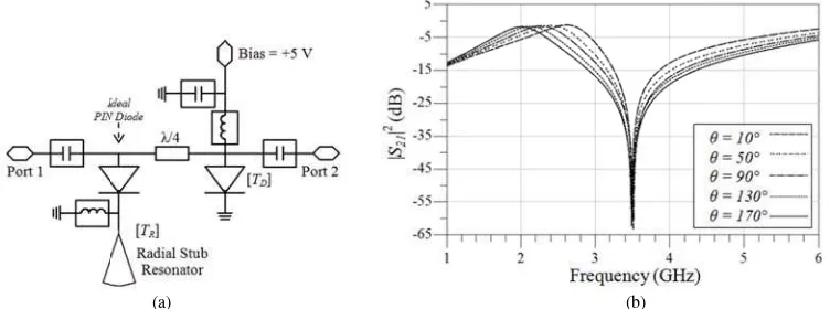
In ON state condition of the PIN diode (Fig. 3 (a)), the RF signal in 50 Ω microstrip line will be short circuited because of low impedance at the input shunt PIN diode due to λ/4 impedance transformation of radial stub (from high to low impedance). The radial stub is equivalent to series inductance and capacitance having a bandstop response between Port 1 and Port 2. In OFF state condition of the PIN diode (Fig. 3 (b)), the radial stub resonator is disconnected from 50 Ω microstrip line having allpass response between input and output port.
As shown in Fig 3 (a), the bandstop response of the radial stub resonator can be modeled using transmission matrix.
| (1)
where Tsis transmission matrix of radial stub resonator, T1is transmission matrix of Microstrip Line at Port 1
and T2is transmission matrix of Microstrip Line at Port 2.
Therefore, we have
cossin cossin tan cossin cossin (2)
Since the impedance of the microstrip lines are 50 Ω, thus they are fully matched with the characteristic impedance of 50 Ω and exhibit very minimum power losses. Therefore T1and T2 can be ignored in order to
simplify the following equation where S parameter of the radial stub resonator can be obtained by converting the transmission matrix in (2) as
| . (3) where Zo is characteristic impedance of microstrip line and Ysis characteristic admittance of radial stub.
The characteristic impedance of radial stub can be obtained as [20]
(4) where d is thickness of substrate, riis inner radial of radial stub and is effective dielectric constant.
The effective dielectric constant of microstrip, can be calculated from [24]
/ (6)
where is relative dielectric constant of substrate. As suggested in [20] for radial stub, W in (6) is calculated as
sin θ (7) Then, rearrange (3) with (4), we get
| π π . (8) To calculate length of radial stub resonator, we know
(9) where
.
Therefore, rearrange (9) and by substituting , the λ/4 length of the radial stub resonator can be determined as
(10) where c is speed of light and f is resonant frequency.
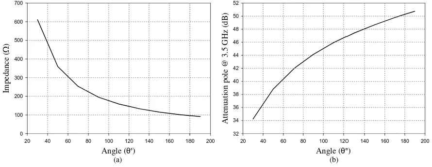
Considering fixed value of d and of printed circuit board (PCB) in (4) and (8), we found that angle, θand inner radius, riof radial stub are significantly influence Zs and S21. Further analysis is carried out using (4) and (8)
by considering resonant frequency at 3.5 GHz and a FR4 substrate having thickness of 1.6 mm and dielectric constant, of 4.7.
As shown in Fig. 4, angle, θis fixed at 90° and inner radius, riis varied in order to observe the correlation
Fig. 5 sh fixed at 1 attenuatio Theref are increa
0
Impeda
nc
e (
)
0 20 40 60 80 100 120 140 160 180 200 220
20
Im
ped
ance (
)
0 100 200 300 400 500 600 700
B. SPDT
A co comparis turned O isolation)
hows the corre 1 mm and ang on pole of S21
fore, we can c ased. This res
2
Fig
40 60
T Switch with
nventional sin son with the p OFF and D2 m
) is obtained s
Fig. 6.
elation of angl gle, θis varied
.
conclude that ult has a poten
Inner Radius (m
4 6
(a)
g. 4. Inner radius,
Angle ()
80 100 120
(a)
Fig. 5. Angle, θ v
Switchable Ra
ngle shunt PI roposed shunt must be turned olely due to O
(a)
. Conventional SP
le, θwith Zs a
d. It is observe higher attenua ntial to impro
mm)
6 8
ri versus (a) char
140 160 18
versus (a) charate
adial Stub Res
IN diode in t SPDT switch d ON . In this ON state of D2
PDT switch. (a) C
and attenuation ed that as the ation pole of S
ve the isolatio
10 0
Atte
nuation pole
@ 3.5 GHz (d
B)
40 45 50 55 60 65
rateristic impedan
80 200 2
Att
enu
at
io
n p
o
le
@ 3.
5
GHz
(dB
)
32 34 36 38 40 42 44 46 48 50 52
eristic impedance
sonator
SPDT switch h. By assumin s condition th
2 in the receive
Circuit design and
n pole of S21.
θ is increased
S21 will be ob
on of SPDT sw
0 2
nce, Zs and (b) att
20 40 60
e, Zs and (b) attenu
h [25] is cons ng the SPDT s he isolation be
e arm.
d (b) isolation bet
In this calcul d it will produ tained if angle witch design.
Inner Radius 4
(b)
tenuation pole of
Angle (
80 100 120
(b)
uation pole of S21
structed (Fig. switch in trans etween Port 1
(b)
tween Port 1 and
lation, inner ra uce lower Zs a
le, θand inner
(mm)
6 8
f S21.
)
0 140 160
1.
6) for a per smit mode, D
1 and Port 2 (
d Port 3.
adius, riis
and higher r radius, ri
10
180 200
rformance
The O us, a simplified
the isolation b eter. Hence,
(12), we know hown that dif screte PIN Dio hunt PIN diod ance between 2
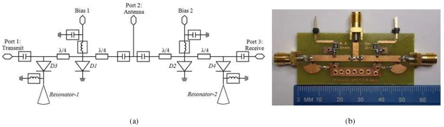
roposed in thi esign. The rad ing a two-port ). A voltage su produce an ad
o-port network of
mple transfer m de in the switch
ng the transfer
isolation can b ulative of isola b) where diff on, the inner ip line and th s wider isolatio cuit diagram a
de-off between and ri is fixed
voltage. nsmit mode (
or-1 becomes op response in n and respons
or-1 are turned
single shunt d transfer matr
between Port
w that isolatio fficult to achie ode in standar de (BAP64-02 2 to 5 GHz. is paper, radia dial stub resona t network con upply of +5 V dditional isola
(a)
f shunt PIN diode
matrix of two hable resonato
r matrix in (13
be obtained if ation of shunt fferent isolatio
radius, ri is
he input of ra on bandwidth and prototype n radial stub at 1.5 mm. A RF signals fr allpass respon
on is obtained eve more than rd package (e.g
from NXP S al stub is used ator is cascade nsist of a shun
is used to tur ation between
e with switchable differ
-port network or. Hence,
3) to S-parame
f and Zs
t PIN diode an on performan fixed at 1.5 dial stub reso
in spite of hig of SPDT swit size and its a All the PIN di rom Port 1 to nse. The D2 an
arm producin ained in the re
2 and Resonato
equivalent to DT switch for
(S31) can be ob
d solely due to n 20 dB of is
e resonator. (a) Ci rent angle of radia
k of the circui
eter, we get
s ≈ 0 in the rad
nd isolation of nce is simula
mm in orde onator. Beside
gh attenuation tch with switc attenuation po
iodes are supp o Port 2), the and Resonator
ng additional eceive mode
or-2 are turne
forward resis isolation analy
. btained by con
. o Rf and Ls of
olation betwe This can be se rs) in SOD52
isolation of t ith the existing and a switchab N diode and the
rt 2.
ircuit diagram an al stub.
it in Fig. 7 (a)
. dial stub reson f the radial stu ated with diff er to minimiz es, it is obser n pole. chable radial s
le performanc plied with +5
D1 and Reso r-2 are turned
isolation (bet (RF signals f d OFF.
stance (Rf) and
ysis is given b nverting the tr f the ON state een Port 1 and
een in Fig. 6 ( 3 package sho the single shu g PIN diode. T ble radial stub e radial stub r
(b)
d (b) isolation be
) is analyzed b
.
nator where th ub resonator. T ferent angle o ze any RF co
rved that larg stub resonator ce, the angle o
V (ON state)
onator-1 are t ON. Then, the tween Port 1 from Port 2 to
d series induc by
ransfer matrix e of shunt PIN d Port 3 if usi (b) where the hows very low unt PIN diode This can be an b resonator as resonator. The
etween Port 1 and
by considerin
he total isolati This can be ob
of radial stub oupling effect ger angle of r r are depicted
of radial, ) and -5 V (O turned OFF. e Resonator-2
and Port 3). ing single simulated w isolation e in SPDT nalyzed by shown in e resonator
d Port 2 with
g an ideal
(13)
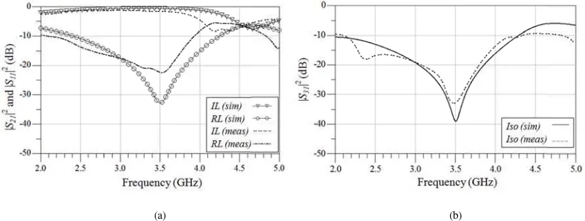
Fig. 9 SPDT sw SPDT sw switch sh compared
Fig. 9. Si
The p switchabl loss and i
Fig. 1 successfu simulatio slightly l specificat
Fig. 8.
shows the sim witch and SPD witch are com hows a signif d with the con
mulated (a) inser
performance c le radial stub isolation.
10 shows the ully demonstra on and measur
lower compar tion of return
(a)
SPDT switch wi
III mulated result DT switch with mparable with
ficant improve nventional SPD
(a)
rtion loss, return l
comparison at resonator are
Convention switch Shunt SPD switchable resonator
simulated and ate an isolatio rement show a red with simu
loss.
th switchable rad
I.SIMULATION
ts of insertion h switchable r the conventio ement of isol DT switch.
loss and (b) isolat switcha
3.5 GHz betw listed in Table
Performan
nal shunt SPDT
DT switch with e radial stub
d measured re n higher than a comparable i ulated ones. H
dial stub resonato
N AND MEASU
n loss (IL), ret radial stub res onal SPDT sw lation which i
tion between sing able radial stub re
ween the conv e I. The perfo
TABLE I ance comparison a
Insertion Loss
0.88 dB
0.65 dB
esult of SPDT 20 dB at 3.5 G insertion loss However, it i
r (a) circuit diagr
UREMENT RESU
turn loss (RL) sonator. The s witch. The sim
is higher than
gle shunt SPDT s esonator.
ventional SPD ormance is com
at 3.5 GHz
Return Loss
29 dB
32.7 dB
switch with s GHz compare and isolation is still higher
(b
ram (b) circuit pro
ULT
) and isolation simulated IL a mulated ISO n 20 dB betw
(b)
witch (conventio
DT switch and mpared betwee
Tx-Rx Isolation
11.5 dB
39 dB
switchable rad ed with the con
result but the r than 10 dB
b)
ototype.
n (ISO) of con and RL of the
of the propos ween 3.05 to 3
onal) and SPDT sw
d the SPDT sw en insertion lo
dial stub reson nventional cir
measured retu B which is a
nventional proposed sed SPDT 3.85 GHz
witch with
witch with oss, return
imulation and me
tchable radial ntial applicati chable radial atical modelin de with switch characteristic Finally, we suc on result which
work describe Therefore, we rowave Labo ment of the res
ou; Jianyi Zhou;
(MTT), 2012 IEE
mmed Younssi; A na for Radiolocati 012.
rnikman; B. H. A Antenna Design",
a, Z.; Ahmad, B
ational , pp.87-90
n, M.H.; Meor Sa ier for WLAN ap
, S. A. Z.; Shahi sion mixer for wi ndle, "The State o N.A.; Ahmad, B for wireless data Bahl and Prakash hara, Y.; Amasug tor," Microwave
N.A.; Ahmad, B tub resonator at 2
, M.; , "An Ana stub resonator," P
(a)
easurement result
stub resonato ion is TDD sw
stub was an ng. Then, the hable radial stu
c impedance ccessfully fab h shows an iso
ed in this pap e would like to oratory, Facul search works.
Zhiming Xu; , "
EE MTT-S Interna
Achraf Jaoujal; A ion Applications,
Ahmad; M. Z. A.
, International Jo
.H.; , "Design of 0, 12-14 Dec. 201 aid, M.A.; Cheng pplication," Green
imin, M. M.; Pok ireless application of RF and Microw B.H.; Khang, A.C
communication, Bhartia, Microw ga, H.; Goto, S.;
Symposium Dige B.H.; Zakaria, Z. 2 GHz band," Wir
lysis of Gap in M 96, Jun 1972. rostrip Reactive C
M. K. A.; Majid, 7–1412, 2012.
ari, and H. Abba
Progress In Elect
of SPDT swith (
IV or is proposed
witching for W nalyzed in te isolation impr ub resonator. T
and attenuatio ricated the SP olation improv
AC
per was fully o acknowledge lty of Electro
"Design of a high
ational , pp.1-3, 1
Ahmed El Mous ," International J
Abd Aziz; A. R.
ournal of Electron
f SIW bandpass 1.
g, K.G.; Othman,
n and Ubiquitous
kharel, R. K.; Ka ns," Microw. Opt
wave Switches", M
C.Z.; , "Design an " RF and Microw
ave Solid State C Oku, T.; Ishikaw est, 2008 IEEE M
; Peng Wen Won
reless Technology
Microstrip Trans
Circuit Elements
H. A.; , "Wideba
asi, "Compact mi
romagnetics Rese
(a) double switcha resonator.
V.CONCLUSIO
in SPDT disc WiMAX and L
erm of chara rovement was There is a cor on pole, thus PDT switch w
vement highe
CKNOWLEDGM
supported by e the contribut onics and Co REFERENCES h performance R 17-22 June 2012. ssaoui; Noura A
Journal of Engine
. Othman; , "Rho
nics and Compute
filter with 6 dB
, M.A.; Ismail, M
s Technology (G
anaya, H. and Y
t. Technol. Lett., 5
Microwave Journ
nd analysis of bro
wave Conference
Circuit Design, Ho wa, T.; , "60GHz MTT-S Internation ng; , "Isolation i
y and Application
smission Lines,"
s," Microwave Th
and to narrowban
icrostrip lowpass
earch Letters, Vo
able radial stub re
ON
crete switch at LTE commun acteristic impe
s analyzed wi rrelation betwe
provide an a with switchable er than 20 dB b
MENT
y Universiti T tion of our col omputer Engin
S
RF transceiver for .
Aknin; , "Miniatu
eering and Techn
ombic Split Ring
er Science Engin
B offset," RF and
M.M.; Sulaiman,
UT), 2012 Intern
oshida, K.; , "Lin 54: 923–925, 201
nal, November 20 oadband high iso
(RFM), 2011 IEE
oboken, NJ: John z High Isolation nal , pp.1541-154 improvement of
ns (ISWTA), 2012
Microwave Theo
heory and Techn
nd frequency reco
filter with sharp ol. 35, 73-81, 201
(b)
esonator and (b) s
t 3.5 GHz for nication system
edance and a ith two-port n een inner radi additional isol e radial stub re between 3.05
Teknikal Mala lleagues from neering, UTeM
r TDD-LTE syste
urized Probe-Fed
ology (IJET), Vo
Resonator (R-SR
eering (IJECSE),
d Microwave Con
H.A.; , "Design
ational Conferen
nearity improvem 12.
007, Vol. 53, No. olation of discrete
EE International
n Wiley & Sons, 2 SPDT MMIC sw 4, 15-20 June 20 SPDT discrete sw
2 IEEE Symposiu
ory and Techniqu
niques, IEEE Tra
onfiguration usin
p roll-off and wid 2.
single switchable
isolation impr m. The charac attenuation p network of sin
ial and angle r olation in SPD
resonator to va to 3.85 GHz.
aysia Melaka Fabrication L eM for fabric
tem," Microwave
d Elliptical Micr ol 4 No 5, page 32
RR) Structure on , Vol. 2, No. 1, p
nference (RFM),
n of Gaas E-phem
nce on , pp.106-1
ment of 5.2-GHz
11, page 20. e packaged PIN
, pp.91-94, 12-14 2003. Chapter 12 witches using sh 008.
witch with single
um on , pp.51-55,
ues, IEEE Trans
ansactions on , v
ng PIN diode," M
de stopband usin
e radial stub
rovement. cteristic of ole using ngle shunt radial stub DT switch alidate the
(UTeM). Laboratory cation and
e Symposium
ostrip Patch 24-327,
Oct-Rectangular age 322-330,
2011 IEEE
mt low noise 09, 7-8 July
z CMOS
up-diode SPDT 4 Dec. 2011. 2.
unt pHEMT
e switchable , 23-26 Sept.
sactions on ,
vol.31, no.6,
Microw. Opt.
[16] Zhebin Wang; Chan-Wang Park; , "Novel wideband GaN HEMT power amplifier using microstrip radial stub to suppress harmonics,"
Microwave Symposium Digest (MTT), 2012 IEEE MTT-S International , pp.1-3, 17-22 June 2012.
[17] Yong-sheng Dai; Da-Gang Fang; Yong-Xin Guo; , "A Novel Miniature 1–22 GHz 90° MMIC Phase Shifter with Microstrip Radial Stubs," Microwave and Wireless Components Letters, IEEE , vol.18, no.2, pp.109-111, Feb. 2008.
[18] Rizk, J.B.; Rebeiz, G.A.; , "W-band microstrip RF-MEMS switches and phase shifters," Microwave Symposium Digest, 2003 IEEE
MTT-S International , vol.3, pp. 1485- 1488 vol.3, 8-13 June 2003.
[19] Yunus, N.A.M.; Wagiran, R.; Postoyalko, V.; , "Design of a microstrip SPDT PIN diode switch," Semiconductor Electronics, 2002.
Proceedings. ICSE 2002. IEEE International Conference on , pp. 465- 469, 19-21 Dec. 2002.
[20] March, S.L.; , "Analyzing Lossy Radial-Line Stubs (Short Papers)," Microwave Theory and Techniques, IEEE Transactions on , vol.33, no.3, pp. 269- 271, Mar 1985.
[21] Naglich, E.J.; Juseop Lee; Peroulis, D.; Chappell, W.J.; , "Switchless Tunable Bandstop-to-All-Pass Reconfigurable Filter," Microwave
Theory and Techniques, IEEE Transactions on , vol.60, no.5, pp.1258-1265, May 2012.
[22] Adoum, B.A.; Wen, W.P.; , "Investigation of band-stop to all pass reconfigurable filter," Intelligent and Advanced Systems (ICIAS),
2012 4th International Conference on , vol.1,.190-193, 12-14 June 2012.
[23] Zahari, M. K.; Ahmad, B. H.; Shairi, N. A.; Peng Wen Wong; , "Reconfigurable dual-mode ring resonator matched bandstop filter,"
Wireless Technology and Applications (ISWTA), 2012 IEEE Symposium on , vol., no., pp.71-74, 23-26 Sept. 2012.
[24] D. M. Pozar, Microwave Engineering. Hoboken, NJ: John Wiley & Sons, 2005. page 144 -145.
![Fig. 2. (a) The proposed switchable radiall stub using PIN ddiode and (b) geoometric of radial sstub [20]](https://thumb-ap.123doks.com/thumbv2/123dok/545214.63743/2.595.83.516.584.731/proposed-switchable-radiall-using-ddiode-geoometric-radial-sstub.webp)