A Study on the depoSition of tin on the
ContACtS SubjeCted to high frequenCy impACt
LoAding in SemiConduCtor deviCe teSting
K.y. ong1, md. radzai Said2
1,2Faculty of Mechanical Engineering, Universiti Teknikal Malaysia Melaka,
Hang Tuah Jaya, 76100 Durian Tunggal, Melaka, MALAYSIA
Email: 1[email protected], 2[email protected]
ABSTRACT
Semiconductor device leads were previously plated with Lead (Pb). Due to environmental concern, the plating material has been switched to Tin (Sn). However, due to the sotness of Tin element plating, it oten wears of and its residues deposited to the surface of the contacts used in semiconductor device testing. As a result, signiicant drop of contact performance has been observed. This study intends to ind out a theoretical explanation to the problem of tin deposition. As soon as the root cause is identiied, studies go into the details of how to solve this problem. One of the economical suggestions is to apply lubricants on the contact. A theoretical calculation is derived to verify if the lubricant would signiicantly altered the overall resistance.
KEYWORDS: Contact, tin, adhesive wear, semiconductor device testing.
1.0 introduCtion
To date, the phenomenon of tin deposition on the electric contacts used in semiconductor device testing is still not very well understood in the industry. Prior to going into the phenomenon itself, it is convenient to irst understand the problem from the basics.
There are many testing methods available in the market. Some uses electro-pneumatic machine to pick semiconductor devices up and place them on electric contacts (or contactors) connected to a tester machine, the tester machine will read the semiconductor device and determine whether it is “good” or “bad”, this type of testing is oten called the pick and place method in the industry. Another popular type of testing is using gravitational force to draw the semiconductor devices downwards, as they passes through the electric contacts at the botom which are also connected to the tester machine; they will be veriied and sorted out. This type of testing method is industrially known as gravity fed method.
Common to all testing methods, the semiconductor device’ leads or pads must touches with the electric contacts (which can be either contacting blades or pogo pins depends on application) so that the current could low through the device. The technology today has enable the process of picking, placing semiconductor devices on electric contacts for testing and picking it up from electric contacts to be done in merely 0.09 seconds. In this particular case, an electric contact is subjected to approximately 11 impact loadings from the leads of the semiconductor device in just one second.
Although achieving very high unit per hour (UPH) performance, there is still one serious issue bothering the engineers. It is found that there are always some tin residues deposited on the electric contacts ater several cycles of testing. The tin residues come from the plating material of the semiconductor device leads or pads. The increase of tin deposition on the contacts brings about an increase of electrical contact resistance as the contacting cycles increases. The usual practice has been to clean the contacts by grinding of the tin residues. However, this measure causes considerable damage to the contacts itself.
Thus, this paper studies about the possible root cause of the deposition or adhesion of tin on contacts used in semiconductor testing.
2.0 LiterAture review
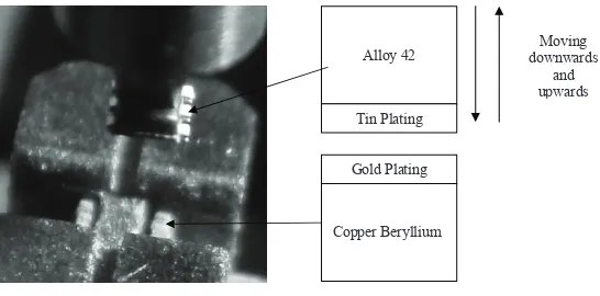
for diferent applications, such as Copper Beryllium, Nickel Beryllium, Tungsten, and some with Gold or Rhodium plating.
FIGURE 1 Contact materials
Alloy 42
Copper Beryllium Tin Plating
Gold Plating
Moving downwards
and upwards
FIGURE 1: Contact materials
There are various perspectives are being looked upon to identify why tin deposited on the contacts. It bears resemblance to solid-state welding, it can be seen as an adhesive wear, and the volume of wear can be calculated.
The irst concept to be taken serious atention is the concept of asperity. It has to be accepted that no surface are perfect. In practice, there are no ideal surfaces which are completely lat. So, it should be accepted that in certain level of magniication, the truth that surfaces are all rough and uneven. Such uneven surfaces are called asperity.
Beginning with the problem of Tin deposition, the direct contact of the electric contacts with the semiconductor device leads can be understood in three levels of complexity, namely:
• simple lead-to- contact contacting
• lead-to- contact impact contacting
• lead-to- contact impact contacting with current
Also, there is a high possibility of sliding contact between the lead to electric contact contacting, which will also be taken into consideration.
According to Kalpakjian (2006), it is essential that the interface be free of oxide ilms, residues, metalworking luids, other contaminants to form a strong bond. Based on the criteria mentioned, it is easy to imagine that heat generated through friction improves the transfer of atoms across an interface. Relative interfacial movements of the contacting surfaces occur, even at very small amplitudes will disturb the mating surfaces which will break up any oxide ilms, and generate new clean surfaces which improve the strength of the bond. If the pressure is high enough, plastic deformation will occur at the interface also promote stronger bonding. Experiments also reveal that when adhesion measurements are performed in vacuum, where the degree of surface contamination is reduced and adhesion between metals become very large (Bowden., and Rowe, 1956). Hence, summarizing from the experience gained from solid-state welding, the following criteria inluences the bond strength of solid-state welding:
• Pressure applied to the interface of contacting
surfaces
• Cleanliness of the contacting surfaces
• Heat generated from internal friction between
contacting surface
• Relative interfacial movements that breaks up the contaminants
• Air density (strongest adhesion occurs in vacuum)
The deposition of tin on the electric contacts could also be a result of adhesion or adhesive wear which is already being studied extensively in the ield of tribology. Adhesive wear occurs as a result of the transfer of soter metal (weak material) to the harder metal (stronger material) by means of friction. (Stachowiak and Batchelor, 2005).
The question of practical interest is what properties of metal that favour such adhesive wear?
Buckley (1981) discovered that greatest adhesion occur between like materials. Iron to iron adhesion for example exhibits the ratio of adhesion force to contact force which can be as high as 20.
Crystal structure also inluences the adhesive strength. Metals with hexagonal close packed structure show much less adhesion than other crystal structures (Sikorski, 1963). This is because hexagonal closed pack metals have far fewer slip systems and are therefore less ductile than face-centered and body centered metals.
High hardness, large elastic moduli and surface energy of metals also suppress adhesion too (Sikorski, 1963). Apart from that, adhesive strength is also a function of the chemical reactivity of metals. Chemical reactivity is oten deined as values in electropositivity. Chemically active metals such as aluminium bond more readily and there show stronger adhesion than noble metals.
Summarizing from the study conducted the material properties of practical importance in contributing to the efect of adhesive wear are divided into mechanical properties and chemical properties. The mechanical properties are
• Crystal structure
• Hardness
• Elastic Modulus
• Surface Energy
Meanwhile, the chemical properties are:
• Electron density
• Chemical Reactivity
The severity of wear can be determined by how much volume of material is rubbed of or carried of from the origin material. There is a mathematical relationship described by Archard equation as a means to determine wear volume as shown in Equation 1. (Harris, 2002) • Crystal structure
• Hardness • Elastic Modulus • Surface Energy
• Electron density • Chemical Reactivity
H KWL
Q= (
• Crystal structure • Hardness • Elastic Modulus • Surface Energy
• Electron density • Chemical Reactivity
= (1)
3.0 diSCuSSion
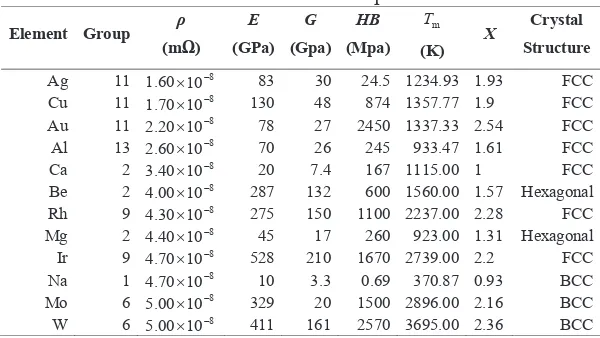
TABLE 1: Material Properties
Element Group ρ (mΩ)
Since, the hardness is of central importance of a contact, Gold, Iridium and Mobylenum may well
+ + + =
Since, the hardness is of central importance of a contact, Gold, Iridium and Mobylenum may well be the alternative substitutes for Copper.
As seen from the study above, the principal reason for wear is a result of the sotness of tin plating itself. However, the tin plating is already a standard plating material for semiconductor device lead. Hence, the only thing can be altered is the contact itself, be it by changing the material, changing the surface treatment or using lubricants.
Instead of changing the building material or surface treatment of the material, it is easier if not beter to try lubrication. Lubrication can be a good solution as it is known that lubricants reduce wear rate. However, it is of engineering interest that whether lubrication would reduce the overall electrical conductivity of the contact. Since lubricant constitute a thin layer of electric contact itself, one important aspect to consider is whether such thin layer of lubricant afect the overall electrical resistance of the contact as the electrical resistance is of primary importance for the system itself.
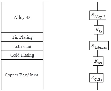
Since resistance elements are in series of each other, the total resistance of the system before lubricant is added would be
FIGURE 2 Resistance model of contact materials with an addition of lu
+
Copper Beryllium Tin Plating
Gold Plating
Lubricant RLubricant
Sn
FIGURE 2: Resistance model of contact materials with an addition of lubricant
When a layer of lubricant is added as shown in Figure 2, the total resistance would change to
CuBe
(1995), resistance is mathematically defined as
A
According to Bueche (1995), resistance is mathematically deined as +
er compared to
≅
cant, L in common sense would be very much sma
≅
Since the thickness of the lubricant, L in common sense would be very much smaller compared to the thicknesses of contact and lead, it is assumed that L is close to zero, i.e.
+
e resistance of the lubricant wou
( ≅ )≅
Journal of Mechanical Engineering and Technology
ρ =
≅
( ≅ )≅ =ρ
( ≅ )+ + ≅ + + + ≅
+ + = ′
T
T R
R ′≅
∴
is not significantly altered.
ρ =
≅
( ≅ )≅ =ρ
( ≅ )+ + ≅ + + + ≅
+ + = ′
≅ ′
∴ (8)
The overall resistance of the system is not signiicantly altered.
4.0 ConCLuSion
As seen from the study above, the principal reason for wear is hypnotized as a result of the sotness of tin plating itself. However, the tin plating is already a standard plating material for semiconductor device lead. Hence, the only thing can be altered is the contact itself, be it by changing the material, changing the surface treatment or using lubricants. Since changing the surface treatment and material takes a very long time and not necessarily an economical way, lubricant may be recommended. Testing will be conducted in the future to verify the proposed hypothesis.
5.0 SymboLS
Q total volume of wear debris produced
W total normal load
H hardness of the sotest contacting surfaces
K dimensionless constant L sliding length
electrical resistance before lubrication electrical resistance ater lubrication
electrical resistance of Alloy 42
electrical resistance of tin
electrical resistance of lubricant
electrical resistance of gold
electrical resistance of copper beryllium
electrical resistance resistivity
length/thickness ross-sectional area
lubricant thickness
6.0 ACKnowLedgement
tolerant and wise mentor. Thanks to Ismeca, especially Mr. SH Chong for initiating this collaboration between Ismeca and UTeM. Special thanks to Mr. Masjuri for his discussion which lead to the birth of such collaboration.
7.0 referenCeS
Buckley, D. H. 1981. Surface efects in adhesion, friction, wear and lubrication. Elsevier.
Epistola, E. 2006. What is a semiconductor. Silicon Far East. Retrieved from April 9, 2010 from htp://www.siliconfareast.com/whatissemicon.htm. Harris, C. K., Broussard, J. P. and Whitcomb, P. J 2002. Determination of wear
in a tribo-system. Proceedings of the 2002 ASEE Gulf-Southwestern Annual Conference.
Kalpakjian, S. 2006. Manufacturing engineering and technology (5th edition). Singapore: Prentice Hall.
Sikorski,M.E. 1963. Correlation of the coeicient of adhesion with various physical and mechanical properties of metals, Transactions ASME, Series D - Journal of Basic Engineering, Vol. 85, pp. 279-285.
Stachowiak, G. W. and Batchelor, A. W. 2005. Engineering tribology (3rd edition). Burlington:Elsevier Buterworth-Heinemann.