Design with PLDs and FPGAs Laboratory(11EC312L)
DESIGN AND IMPLEMENTATION OF
TRAFFIC LIGHTS CONTROLLER
USING FPGA
A Project Based Laboratory Report
in partial fulfilment for the award of III/IV B.Tech I Semester
Submitted by
S.Najia tasleem (Reg. No.12004338) P.Manasvi (Reg. No. 12004339)
D.Teja sri (Reg. No. 12004341) R.Monica (Reg. No. 12004343)
Lab Instructor
Dr.Fazal NoorBasha
Department of ECE,
Department of Electronics and Communication Engineering
KL University, Vaddeswaram, Guntur, AP – 522502
C E R T I F I C A T E
DECLARATION
We declare that the project entitled, “DESIGN AND IMPLEMENTATION
OF TRAFFIC LIGHTS CONTROLLER USING FPGA” is our own work
conducted under the esteemed guidance of Dr. Fazal Noorbasha (Section
Instructor), Dr. Harikishore K, Mr.B.Kali Vara Prasad and Ms. M Preeti, at
the Department of Electronics and Communication Engineering of KL
University, Vaddeswaram, Guntur, A.P., INDIA.
ACKNOWLEDGEMENT
Working on this Project based Lab is certainly a memorable and enjoyable event in our life. We have learned a lot of interesting new things that have broadened our view of the technology field. In here, we would like to offer our appreciation and thanks to several grateful and helpful individuals. Without them, this work could not have been completed and the experience would not be so enjoyable.
We are very grateful to our esteemed Professors Dr. Fazal Noorbasha (Section Instructor), Dr. K Harikishore, Mr.B.Kali Vara Prasad and Ms. M Preeti, Department of ECE, KL University, Vaddeswaram, Guntur, A.P., INDIA, for their valuable guidance and creative suggestions that helped us to complete this Lab project.
Furthermore, we are also very thankful Dr. Fazal Noorbasha, Microelectronics Group Head, to have an opportunity to learn from him on the aspect of using the advancing FPGA technology to improve the performance for different memory and processor applications. Hopefully, this experience will inspire us to come up with new and interesting research ideas in the future.
Furthermore, we want to offer our thanks to Dr. ASCS Sastry, Professor & Head, Department ECE, KL University, Vaddeswaram, Guntur, A.P., INDIA, for providing the required facilities to carry out the project work successfully.
We would like to thank all those helped us directly or indirectly during this
project work.
D.Teja sri (Reg. No. 12004341) R.Monica (Reg. No. 12004343)
ABSTRACT
The traffic in road crossings /junctions is controlled by switching ON/OFF
Red, Green & Amber lights in a particular sequence. The Traffic Light
Controller is designed to generate a sequence of digital data called switching
sequences that can be used to control the traffic lights of a typical four
roads junction in a fixed sequence. It is also proposed to implement the day
mode and night mode operations. It plays more and more important role in
modern management and control of urban traffic to reduce the accident and
traffic jam in road. It is a sequential machine to be analyzed and
programmed through a multistep process. The device that involves an
analysis of existing sequential machines in traffic lights controllers, timing
and synchronization and introduction of operation and flashing light
synthesis sequence. The methods that are used in this project are design the
circuit, write a coding, simulation, synthesis and implement in hardware. In
this project, XILINX Software was chosen to design a schematic using
schematic edit, writes a coding using Verilog HDL (Hardware Description
Language) text editor and implements the circuit on Programmable Logic
LIST OF FIGURES
Fig. No. Title Page No
1.1 FPGA Design Flow 3
1.2 FPGA Synthesis 4
1.3 FPGA Translate 5
1.4 FPGA Map 6
1.5 FPGA Place and route 6
2.1 TLC Flow Chart 8
2.2 Traffic Signals at Junction 9
2.3 TLC State Diagram 11
3.1 RTL Schematic 13
3.2 Technology Schematic 14
3.3 Wave Form 15
4.1 Structure of Road 16
4.2 Spartan3E trainer kit 17
CONTENTS
Certificate i
Declaration ii
Acknowledgements iii
Abstract iv
List of Figures V
List of Tables Vi
Contents Vii
Chapter – 1
Introduction 1-2
1.1 Traffic lights 1
1.2 Electronic design with FPGA’S 2
1.3 FPGA design flow 3
Chapter – 2
System Block Diagram and Working Principle 3-4
2.1 System block diagram 3
2.2 Working Principle 4
Chapter – 3 5-6
System Modeling 5
Chapter – 4
Implementation results 7-8
4.1 System Analysis 7
4.2 Results Report 8
Chapter 5
Conclusions and Applications 9-10
5.1 Conclusion 9
5.2 Applications 10
Appendix 11-13
Appendix – A: Verilog Code and Test Bench 11
Chapter – 1 INTRODUCTION
1.1 Need for Traffic Light Controller
simplified timing No test vectors Relaxed verification
Physical design is “handsoff”
FPGA is an Integrated Circuit consisting of an array of uncommitted elements; interconnection between these elements is userprogrammable. Using Random Access Memory, high density logic is provided. FPGA is the source code, ChipScope ProIntegrated Controller (ICON) and Virtual Input Output (VIO).
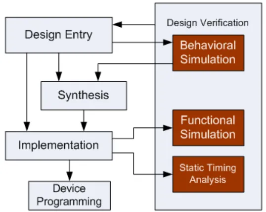
1.3 FPGA Design Flow
Design Entry details of the hardware implementation. Schematic based entry gives designers much more visibility into the hardware. It is the better choice for
design element
Synthesis process will check code syntax and analyze the hierarchy of the design which ensures that the design is optimized for the design architecture, the designer has selected. The resulting netlist(s) is saved to an NGC( Native Generic Circuit) file (for Xilinx® Synthesis Technology (XST)).
Implementation
This process consists a sequence of three steps 1. Translate
2. Map
3. Place and Route
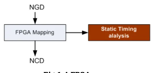
Translate process combines all the input netlists and constraints to a logic design file. This information is saved as a NGD (Native Generic Database) file. This can be done using NGD Build program. Here, defining constraints is nothing but, assigning the ports in the design to the physical elements (ex. pins, switches, buttons etc) of the targeted device and specifying time requirements of the design. This information is stored in a file named UCF (User Constraints File).
Tools used to create or modify the UCF are PACE, Constraint Editor etc.
Fig 1.3 FPGA Translate
Fig 1.4 FPGA map
Place and Route PAR program is used for this process. The place and route process places the sub blocks from the map process into logic blocks according to the constraints and connects the logic blocks. Ex. if a sub block is placed in a logic block which is very near to IO pin, then it may save the time but it may affect some other constraint. So trade off between all the constraints is taken account by the place and route process. The PAR tool takes the mapped NCD file as input and produces a completely routed NCD file as output. Output NCD file consists the routing information.
Fig 1.5 FPGA Place and route
Device Programming
Now the design must be loaded on the FPGA. But the design must be converted to a format so that the FPGA can accept it. BITGEN program deals with the conversion. The routed NCD file is then given to the BITGEN program to generate a bit stream (a .BIT file) which can be used to configure the target FPGA device. This can be done using a cable. Selection of cable depends on the design.
Design Verification
Behavioural Simulation (RTL Simulation) This is first of all simulation steps; those are encountered throughout the hierarchy of the design flow. This simulation is performed before synthesis process to verify RTL (behavioural) code and to confirm that the design is functioning as intended. Behavioural simulation can be performed on either VHDL or Verilog designs. In this process, signals and variables are observed, procedures and functions are traced and breakpoints are set. This is a very fast simulation and so allows the designer to change the HDL code if the required functionality is not met with in a short time period. Since the design is not yet synthesized to gate level, timing and resource usage properties are still unknown.
Functional simulation (Post Translate Simulation) Functional simulation gives information about the logic operation of the circuit. Designer can verify the functionality of the design using this process after the Translate process. If the functionality is not as expected, then the designer has to made changes in the code and again follow the design flow steps.
Chapter – 2
Design of Traffic Light Controller
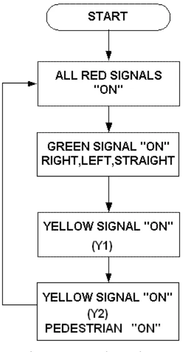
Traffic Light Controller can be designed by starting with some arbitrary assumptions. At first the North traffic will be allowed to move and then traffic in the East, South and West direction will be allowed to move in sequence. The advantage of writing Traffic Light Controller program is that in a program, modifications as per requirements can be done easily i.e., suppose the traffic on main road should be allowed for more time and for side roads the traffic should be allowed for less time; then the clock is divided in such a way that for main road the clock period will be more and for side roads the clock period will be less, this is because the main road traffic is heavy when compared to the side road traffic. In general TLC System will be having three lights (red, green and yellow) in each direction where red light stands for traffic to be stopped, green light stands for traffic to be allowed and yellow light stands for traffic is going to be stopped in few seconds.
2.1 Explanation of Traffic Light Controller
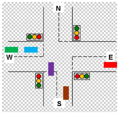
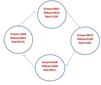
In this structure, there are four traffic signals, represented by R1, R2, R3 and R4 to be controlled. All the four signals have same priority as they all are main roads.
Fig 2.2 Traffic Signals at Junction
First of all the signal controller is in the reset mode where in the signal of road (R1) is green whereas all the other roads R2, R3 and R4 are red. This state we have assigned as S0.
dir=01 then yellow light (y1) will be ON for few seconds and when cnt=01 yellow light (y2) and pedestrian east will be ON and then dir is incremented by one and cnt is assigned to zero.
Fig 2.3 TLC State Diagram
Chapter – 3
Simulation Results
3.1 RTL Schematic
The below figure shows the RTL Schematic of the Traffic Light Controller.
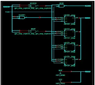
3.2 Technology Schematic
The below figure shows the Technology Schematic of the Traffic Light Controller.
Fig 3.2 Technology Schematic
3.3 Wave Form
Fig 3.3 Wave Form
Chapter – 4
Hardware Implementation
Fig. 4.1 depicts a general four road structure which consists of north, east, west and south directions each with a set of three lights namely green, yellow and red. Green light in a direction will be ON when left, straight and right side is set to be free for traffic in that direction.
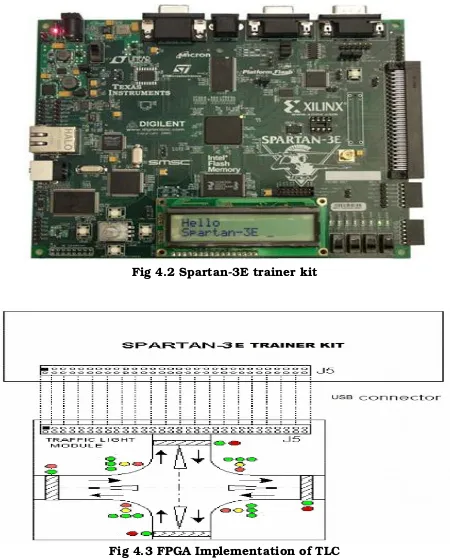
Fig 4.1 Structure of Road
The state machine is coded using the Hardware Description Language, Verilog. Spartan3E trainer kit is shown in Fig. 4.2.
Fig 4.2 Spartan3E trainer kit
Fig 4.3 FPGA Implementation of TLC
Chapter – 5
Implementation Results
The Traffic Light Controller was designed using Verilog HDL and was implemented using FPGA. The output of the TLC is verified with NEXYS 2 FPGA. Fig 5.1 shows the following were the results taken by us after the implementation.
Chapter – 6
Conclusion and Future Scope
The modern ways of multiway traffic management improves the traffic condition up to a large extent. Advanced signaling controllers contribute to the improvement of the urban traffic; which is proportional to the complexity of the controller. These more complex controllers can be well handled using states machines. Methods to reduce the states in the state machine also help in reducing the required hardware thus leading to low power and area efficient design.
The future scope of this project is it can be directly applied in real time by employing more number of such circuits.
Bibliography
grn=4'b0010;
Test bench :
module tb;
// Inputs
reg [1:0] state;