LAMPIRAN A
Features
• Compatible with MCS-51™ Products
• 8K Bytes of In-System Reprogrammable Flash Memory • Endurance: 1,000 Write/Erase Cycles
• Fully Static Operation: 0 Hz to 24 MHz • Three-level Program Memory Lock • 256 x 8-bit Internal RAM
• 32 Programmable I/O Lines • Three 16-bit Timer/Counters • Eight Interrupt Sources • Programmable Serial Channel
• Low-power Idle and Power-down Modes
Description
The AT89C52 is a low-power, high-performance CMOS 8-bit microcomputer with 8K bytes of Flash programmable and erasable read only memory (PEROM). The device is manufactured using Atmel’s high-density nonvolatile memory technology and is compatible with the industry-standard 80C51 and 80C52 instruction set and pinout. The on-chip Flash allows the program memory to be reprogrammed in-system or by a conventional nonvolatile memory programmer. By combining a versatile 8-bit CPU with Flash on a monolithic chip, the Atmel AT89C52 is a powerful microcomputer which provides a highly-flexible and cost-effective solution to many embedded control applications. XTAL2 XTAL1 GND
NC XTAL 2 XTAL1 GND
NC
AT89C52
Block Diagram
PORT 2 DRIVERS
PORT 2 LATCH
P2.0 - P2.7
QUICK FLASH PORT 0
LATCH RAM
PROGRAM ADDRESS REGISTER
BUFFER
PC INCREMENTER
PROGRAM COUNTER
DPTR RAM ADDR.
REGISTER
INSTRUCTION REGISTER B
REGISTER
INTERRUPT, SERIAL PORT, AND TIMER BLOCKS
STACK POINTER ACC
TMP2 TMP1
ALU
PSW
TIMING AND CONTROL
PORT 3 LATCH
PORT 3 DRIVERS
P3.0 - P3.7 PORT 1
LATCH
PORT 1 DRIVERS
P1.0 - P1.7 OSC
GND VCC
PSEN ALE/PROG EA / VPP RST
AT89C52
The AT89C52 provides the following standard features: 8K bytes of Flash, 256 bytes of RAM, 32 I/O lines, three 16-bit timer/counters, a six-vector two-level interrupt architecture, a full-duplex serial port, on-chip oscillator, and clock cir-cuitry. In addition, the AT89C52 is designed with static logic for operation down to zero frequency and supports two software selectable power saving modes. The Idle Mode stops the CPU while allowing the RAM, timer/counters, serial port, and interrupt system to continue functioning. The Power-down mode saves the RAM contents but freezes the oscillator, disabling all other chip functions until the next hardware reset.
Pin Description
Port 0 is an 8-bit open drain bi-directional I/O port. As an output port, each pin can sink eight TTL inputs. When 1s are written to port 0 pins, the pins can be used as high-impedance inputs.
Port 0 can also be configured to be the multiplexed low-order address/data bus during accesses to external pro-gram and data memory. In this mode, P0 has internal pullups.
Port 0 also receives the code bytes during Flash program-mi ng an d ou tpu t s the c o de b y tes du r in g pr o gr a m verification. External pullups are required during program verification.
Port 1
Port 1 is an 8-bit bi-directional I/O port with internal pullups. The Port 1 output buffers can sink/source four TTL inputs. When 1s are written to Port 1 pins, they are pulled high by the internal pullups and can be used as inputs. As inputs, Port 1 pins that are externally being pulled low will source current (IIL) because of the internal pullups.
In addition, P1.0 and P1.1 can be configured to be the timer/counter 2 external count input (P1.0/T2) and the timer/counter 2 trigger input (P1.1/T2EX), respectively, as shown in the following table.
Port 1 also receives the low-order address bytes during Flash programming and verification.
Port 2
Port 2 is an 8-bit bi-directional I/O port with internal pullups. The Port 2 output buffers can sink/source four TTL inputs. When 1s are written to Port 2 pins, they are pulled high by the internal pullups and can be used as inputs. As inputs, Port 2 pins that are externally being pulled low will source current (IIL) because of the internal pullups.
Port 2 emits the high-order address byte during fetches from external program memory and during accesses to external data memory that use 16-bit addresses (MOVX @ DPTR). In this application, Port 2 uses strong internal pul-lups when emitting 1s. During accesses to external data memory that use 8-bit addresses (MOVX @ RI), Port 2 emits the contents of the P2 Special Function Register. Port 2 also receives the high-order address bits and some control signals during Flash programming and verification. Port 3
Port 3 is an 8-bit bi-directional I/O port with internal pullups. The Port 3 output buffers can sink/source four TTL inputs. When 1s are written to Port 3 pins, they are pulled high by the internal pullups and can be used as inputs. As inputs, Port 3 pins that are externally being pulled low will source current (IIL) because of the pullups.
Port 3 also serves the functions of various special features of the AT89C51, as shown in the following table.
Port 3 also receives some control signals for Flash pro-gramming and verification.
RST
Reset input. A high on this pin for two machine cycles while the oscillator is running resets the device.
ALE/PROG
Address Latch Enable is an output pulse for latching the low byte of the address during accesses to external mem-ory. This pin is also the program pulse input (PROG) during Flash programming.
In normal operation, ALE is emitted at a constant rate of 1/6 the oscillator frequency and may be used for external Port Pin Alternate Functions
P1.0 T2 (external count input to Timer/Counter 2), clock-out
P1.1 T2EX (Timer/Counter 2 capture/reload trigger and direction control)
Port Pin Alternate Functions
P3.0 RXD (serial input port)
P3.1 TXD (serial output port) P3.2 INT0 (external interrupt 0)
P3.3 INT1 (external interrupt 1) P3.4 T0 (timer 0 external input)
P3.5 T1 (timer 1 external input)
P3.6 WR (external data memory write strobe)
AT89C52
timing or clocking purposes. Note, however, that one ALE pulse is skipped during each access to external data memory.
If desired, ALE operation can be disabled by setting bit 0 of SFR location 8EH. With the bit set, ALE is active only dur-ing a MOVX or MOVC instruction. Otherwise, the pin is weakly pulled high. Setting the ALE-disable bit has no effect if the microcontroller is in external execution mode.
PSEN
Program Store Enable is the read strobe to external pro-gram memory.
When the AT89C52 is executing code from external pro-gram memory, PSEN is activated twice each machine cycle, except that two PSEN activations are skipped during each access to external data memory.
EA/VPP
External Access Enable. EA must be strapped to GND in order to enable the device to fetch code from external pro-gram memory locations starting at 0000H up to FFFFH. Note, however, that if lock bit 1 is programmed, EA will be internally latched on reset.
EA should be strapped to VC C for internal program executions.
This pin also receives the 12-volt programming enable volt-age (VP P) during Flash programming when 12-volt programming is selected.
XTAL1
Input to the inverting oscillator amplifier and input to the internal clock operating circuit.
XTAL2
Output from the inverting oscillator amplifier.
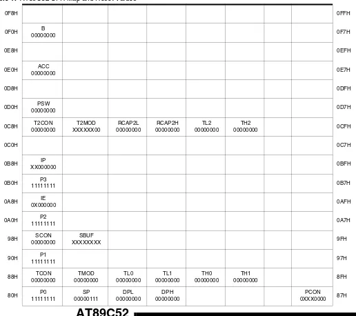
Table 1. AT89C52 SFR Map and Reset Values
AT89C52
Special Function Registers
A map of the on-chip memory area called the Special Func-tion Register (SFR) space is shown in Table 1.
Note that not all of the addresses are occupied, and unoc-cupied addresses may not be implemented on the chip. Read accesses to these addresses will in general return random data, and write accesses will have an indetermi-nate effect.
User software should not write 1s to these unlisted loca-tions, since they may be used in future products to invoke
new features. In that case, the reset or inactive values of the new bits will always be 0.
Timer 2 Registers Control and status bits are contained in registers T2CON (shown in Table 2) and T2MOD (shown in Table 4) for Timer 2. The register pair (RCAP2H, RCAP2L) are the Capture/Reload registers for Timer 2 in 16-bit cap-ture mode or 16-bit auto-reload mode.
Interrupt Registers The individual interrupt enable bits are in the IE register. Two priorities can be set for each of the six interrupt sources in the IP register.r
Data Memory
The AT89C52 implements 256 bytes of on-chip RAM. The upper 128 bytes occupy a parallel address space to the Special Function Registers. That means the upper 128 bytes have the same addresses as the SFR space but are physically separate from SFR space.
When an instruction accesses an internal location above address 7FH, the address mode used in the instruction
specifies whether the CPU accesses the upper 128 bytes of RAM or the SFR space. Instructions that use direct addressing access SFR space.
For example, the following direct addressing instruction accesses the SFR at location 0A0H (which is P2).
MOV 0A0H, #data
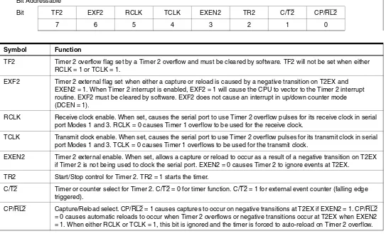
Table 2. T2CON – Timer/Counter 2 Control Registe
T2CON Address = 0C8H Reset Value = 0000 0000B
Bit Addressable
Bit TF2 EXF2 RCLK TCLK EXEN2 TR2 C/T2 CP/RL2
7 6 5 4 3 2 1 0
Symbol Function
TF2 Timer 2 overflow flag set by a Timer 2 overflow and must be cleared by software. TF2 will not be set when either RCLK = 1 or TCLK = 1.
EXF2 Timer 2 external flag set when either a capture or reload is caused by a negative transition on T2EX and EXEN2 = 1. When Timer 2 interrupt is enabled, EXF2 = 1 will cause the CPU to vector to the Timer 2 interrupt routine. EXF2 must be cleared by software. EXF2 does not cause an interrupt in up/down counter mode (DCEN = 1).
RCLK Receive clock enable. When set, causes the serial port to use Timer 2 overflow pulses for its receive clock in serial port Modes 1 and 3. RCLK = 0 causes Timer 1 overflow to be used for the receive clock.
TCLK Transmit clock enable. When set, causes the serial port to use Timer 2 overflow pulses for its transmit clock in serial port Modes 1 and 3. TCLK = 0 causes Timer 1 overflows to be used for the transmit clock.
EXEN2 Timer 2 external enable. When set, allows a capture or reload to occur as a result of a negative transition on T2EX if Timer 2 is not being used to clock the serial port. EXEN2 = 0 causes Timer 2 to ignore events at T2EX.
TR2 Start/Stop control for Timer 2. TR2 = 1 starts the timer.
C/T2 Timer or counter select for Timer 2. C/T2 = 0 for timer function. C/T2 = 1 for external event counter (falling edge triggered).
AT89C52
Instructions that use indirect addressing access the upper 128 bytes of RAM. For example, the following indirect addressing instruction, where R0 contains 0A0H, accesses the data byte at address 0A0H, rather than P2 (whose address is 0A0H).
MOV @R0, #data
Note that stack operations are examples of indirect addressing, so the upper 128 bytes of data RAM are avail-able as stack space.
Timer 0 and 1
Timer 0 and Timer 1 in the AT89C52 operate the same way as Timer 0 and Timer 1 in the AT89C51.
Timer 2
Timer 2 is a 16-bit Timer/Counter that can operate as either a timer or an event counter. The type of operation is selected by bit C/T2 in the SFR T2CON (shown in Table 2). Timer 2 has three operating modes: capture, auto-reload (up or down counting), and baud rate generator. The modes are selected by bits in T2CON, as shown in Table 3. Timer 2 consists of two 8-bit registers, TH2 and TL2. In the Timer function, the TL2 register is incremented every machine cycle. Since a machine cycle consists of 12 oscil-lator periods, the count rate is 1/12 of the osciloscil-lator frequency.
In the Counter function, the register is incremented in response to a 1-to-0 transition at its corresponding external
input pin, T2. In this function, the external input is sampled during S5P2 of every machine cycle. When the samples show a high in one cycle and a low in the next cycle, the count is incremented. The new count value appears in the register during S3P1 of the cycle following the one in which the transition was detected. Since two machine cycles (24 oscillator periods) are required to recognize a 1-to-0 transi-tion, the maximum count rate is 1/24 of the oscillator frequency. To ensure that a given level is sampled at least once before it changes, the level should be held for at least one full machine cycle.
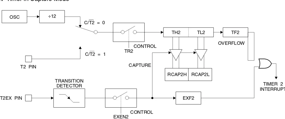
Capture Mode
In the capture mode, two options are selected by bit EXEN2 in T2CON. If EXEN2 = 0, Timer 2 is a 16-bit timer or counter which upon overflow sets bit TF2 in T2CON. This bit can then be used to generate an interrupt. If EXEN2 = 1, Timer 2 performs the same operation, but a 1-to-0 transition at external input T2EX also causes the cur-rent value in TH2 and TL2 to be captured into RCAP2H and RCAP2L, respectively. In addition, the transition at T2EX causes bit EXF2 in T2CON to be set. The EXF2 bit, like TF2, can generate an interrupt. The capture mode is illus-trated in Figure 1.
Auto-reload (Up or Down Counter)
Timer 2 can be programmed to count up or down when configured in its 16-bit auto-reload mode. This feature is invoked by the DCEN (Down Counter Enable) bit located in the SFR T2MOD (see Table 4). Upon reset, the DCEN bit is set to 0 so that timer 2 will default to count up. When DCEN is set, Timer 2 can count up or down, depending on the value of the T2EX pin.
Table 3. Timer 2 Operating Modes
RCLK +TCLK CP/RL2 TR2 MODE
0 0 1 16-bit Auto-reload
0 1 1 16-bit Capture
1 X 1 Baud Rate Generator
AT89C52
Figure 1. Timer in Capture Mode
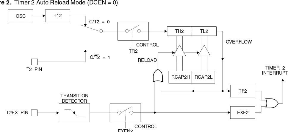
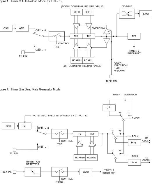
Figure 2 shows Timer 2 automatically counting up when DCEN = 0. In this mode, two options are selected by bit EXEN2 in T2CON. If EXEN2 = 0, Timer 2 counts up to 0FFFFH and then sets the TF2 bit upon overflow. The overflow also causes the timer registers to be reloaded with the 16-bit value in RCAP2H and RCAP2L. The values in Timer in Capture ModeRCAP2H and RCAP2L are preset by software. If EXEN2 = 1, a 16-bit reload can be triggered either by an overflow or by a 1-to-0 transition at external input T2EX. This transition also sets the EXF2 bit. Both the TF2 and EXF2 bits can generate an interrupt if enabled. Setting the DCEN bit enables Timer 2 to count up or down, as shown in Figure 3. In this mode, the T2EX pin controls
the direction of the count. A logic 1 at T2EX makes Timer 2 count up. The timer will overflow at 0FFFFH and set the TF2 bit. This overflow also causes the 16-bit value in RCAP2H and RCAP2L to be reloaded into the timer regis-ters, TH2 and TL2, respectively.
A logic 0 at T2EX makes Timer 2 count down. The timer underflows when TH2 and TL2 equal the values stored in RCAP2H and RCAP2L. The underflow sets the TF2 bit and causes 0FFFFH to be reloaded into the timer registers. The EXF2 bit toggles whenever Timer 2 overflows or underflows and can be used as a 17th bit of resolution. In this operating mode, EXF2 does not flag an interrupt.
OSC
EXF2 T2EX PIN
T2 PIN
TR2
EXEN2 C/T2 = 0
C/T2 = 1
CONTROL
CAPTURE
OVERFLOW
CONTROL TRANSITION
DETECTOR TIMER 2
INTERRUPT ÷12
RCAP2L RCAP2H
AT89C52
Figure 2. Timer 2 Auto Reload Mode (DCEN = 0)
Table 4. T2MOD – Timer 2 Mode Control Register
T2MOD Address = 0C9H Reset Value = XXXX XX00B Not Bit Addressable
– – – – – – T2OE DCEN
Bit 7 6 5 4 3 2 1 0
Symbol Function
– Not implemented, reserved for future T2OE Timer 2 Output Enable bit.
DCEN When set, this bit allows Timer 2 to be configured as an up/down counter.
OSC
EXF2 TF2
T2EX PIN T2 PIN
TR2
EXEN2 C/T2 = 0
C/T2 = 1
CONTROL
RELOAD
OVERFLOW
CONTROL TRANSITION
DETECTOR
TIMER 2 INTERRUPT ÷12
RCAP2L RCAP2H
AT89C52
Figure 3. Timer 2 Auto Reload Mode (DCEN = 1)
Figure 4. Timer 2 in Baud Rate Generator Mode OSC (DOWN COUNTING RELOAD VALUE)
(UP COUNTING RELOAD VALUE)
ULN2801A
ULN2804A - ULN2805A
ULN2802A - ULN2803A
September 1997
EIGHT DARLINGTON ARRAYS
.
EIGHT DARLINGTONS WITH COMMONEMIT-TERS
.
OUTPUT CURRENT TO 500 mA.
OUTPUT VOLTAGE TO 50 V.
INTEGRAL SUPPRESSION DIODES.
VERSIONS FOR ALL POPULAR LOGIC FAMI-LIES.
OUTPUT CAN BE PARALLELED.
INPUTS PINNED OPPOSITE OUTPUTS TO SIMPLIFY BOARD LAYOUTDESCRIPTION
The ULN2801A-ULN2805Aeach contain eight dar-lington transistors with common emitters and inte-gral suppression diodes for inductive loads. Each darlington features a peak load current rating of 600mA (500mA continuous) and can withstand at least 50V in the off state. Outputsmay be paralleled for higher current capability.
Five versions are available to simplify interfacing to standard logic families : the ULN2801A is designed for general purpose applications with a current limit resistor ; the ULN2802Ahas a 10.5kΩinput resistor and zener for 14-25V PMOS ; the ULN2803A has a 2.7kΩinput resistor for 5V TTL and CMOS ; the ULN2804A has a 10.5kΩinput resistor for 6-15V CMOS and the ULN2805A is designed to sink a minimum of 350mA for standard and Schottky TTL where higher output current is required.
All types are supplied in a 18-lead plastic DIP with a copperlead from and featurethe convenientinput-opposite-output pinout to simplify board layout.
DIP18
SCHEMATIC DIAGRAM AND ORDER CODES
For ULN2801A (each driver for PMOS-CMOS) For ULN2802A (each driver for 14-15 V PMOS)
For ULN2804A (each driver for 6-15 V CMOS/PMOS
For ULN2803A (each driver for 5 V, TTL/CMOS)
For ULN2805A (each driver for high out TTL)
THERMAL DATA
Symbol Parameter Value Unit
Rth j–amb Thermal Resistance Junction-ambient Max. 55 °C/W
ELECTRICAL CHARACTERISTICS(Tamb= 25oC unless otherwise specified)
Symbol Parameter Test Conditions Min. Typ. Max. Unit Fig.
ICEX Output Leakage Current VCE= 50V
Tamb= 70°C, VCE= 50V VCE(sat) Collector-emitter
Saturation Voltage
Ii(on) Input Current for ULN2802A Vi= 17V
for ULN2803A Vi= 3.85V
hFE DC Forward Current Gain for ULN2801A
VCE= 2V, IC= 350mA 1000 – 2
Ci Input Capacitance 15 25 pF –
tPLH Turn-on Delay Time 0.5 Vito 0.5 Vo 0.25 1 µs –
tPHL Turn-off Delay Time 0.5 Vito 0.5 Vo 0.25 1 µs –
IR Clamp Diode Leakage Current VR= 50V
Tamb= 70°C, VR= 50V
ABSOLUTE MAXIMUM RATINGS
Symbol Parameter Value Unit
Vo Output Voltage 50 V
Vi Input Voltage
for ULN2802A, UL2803A, ULN2804A
for ULN2805A 3015
V
IC Continuous Collector Current 500 mA
IB Continuous Base Current 25 mA
Ptot Power Dissipation
(one Darlington pair) (total package)
1.0 2.25
W
Tamb Operating Ambient Temperature Range – 20 to 85 °C
Tstg Storage Temperature Range – 55 to 150 °C
Tj Junction Temperature Range – 20 to 150 °C
TEST CIRCUITS
Figure 1a. Figure 1b.
Figure 2. Figure 3.
Figure 4. Figure 5.
Figure 6. Figure 7.
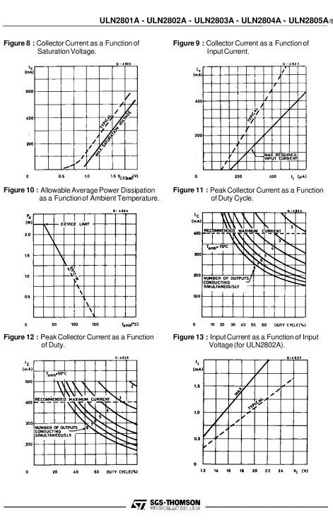
Figure 8 :Collector Current as a Function of Saturation Voltage.
Figure 9 :Collector Current as a Function of Input Current.
Figure 10 :Allowable Average Power Dissipation as a Function of Ambient Temperature.
Figure 11 :Peak Collector Current as a Function of Duty Cycle.
Figure 12 :Peak Collector Current as a Function of Duty.
Figure 13 :Input Current as a Function of Input Voltage (for ULN2802A).
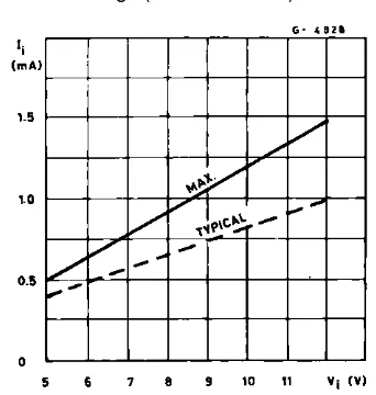
Figure 14 :Input Current as a Function of Input Voltage (for ULN2804A)
Figure 15 :Input Current as a Function of Input Voltage (for ULN2803A)
Figure 16 :Input Current as a Function of Input Voltage (for ULN2805A)
DIP18 PACKAGE MECHANICAL DATA
DIM. mm inch
MIN. TYP. MAX. MIN. TYP. MAX.
a1 0.254 0.010
B 1.39 1.65 0.055 0.065
b 0.46 0.018
b1 0.25 0.010
D 23.24 0.915
E 8.5 0.335
e 2.54 0.100
e3 20.32 0.800
F 7.1 0.280
I 3.93 0.155
L 3.3 0.130
Z 1.27 1.59 0.050 0.063
CMPS03 - Robot Compass Module
This compass module has been specifically designed for use in robots as an aid to
navigation. The aim was to produce a unique number to represent the direction
the robot is facing. The compass uses the Philips KMZ51 magnetic field sensor,
which is sensitive enough to detect the Earths magnetic field. The output from
two of them mounted at right angles to each other is used to compute the
direction of the horizontal component of the Earths magnetic field.
Connections to the compass module
The compass module requires a 5v power supply at a nominal 15mA.
There are two ways of getting the bearing from the module. A PWM signal is
available on pin 4, or an I2C interface is provided on pins 2,3.
The PWM signal is a pulse width modulated signal with the positive width of the
pulse representing the angle. The pulse width varies from 1mS (0° ) to 36.99mS
(359.9 ° ) – in other words 100uS/° with a +1mS offset. The signal goes low for
65mS between pulses, so the cycle time is 65mS + the pulse width - i.e.
66ms-102ms. The pulse is generated by a 16 bit timer in the processor giving a 1uS
resolution, however I would not recommend measuring this to anything better
than 0.1° (10uS). Make sure you connect the I2C pins, SCL and SDA, to the 5v
supply if you are using the PWM, as there are no pull-up resistors on these pins.
I2C communication protocol with the compass module is the same as popular
eeprom's such as the 24C04.. First send a start bit, the module address (0XC0)
with the read/write bit low, then the register number you wish to read. This is
followed by a repeated start and the module address again with the read/write bit
high (0XC1). You now read one or two bytes for 8bit or 16bit registers
respectively. 16bit registers are read high byte first. The compass has a 16 byte
array of registers, some of which double up as 16 bit registers as follows;
Register
Function
0 Software Revision Number
1 Compass Bearing as a byte, i.e. 0-255 for a full circle
2,3 Compass Bearing as a word, i.e. 0-3599 for a full circle, representing
0-359.9 degrees.
4,5 Internal Test - Sensor1 difference signal - 16 bit signed word
6,7 Internal Test - Sensor2 difference signal - 16 bit signed word
8,9 Internal Test - Calibration value 1 - 16 bit signed word
10,11 Internal Test - Calibration value 2 - 16 bit signed word
12 Unused - Read as Zero
13 Unused - Read as Zero
14 Unused - Read as Undefined
15 Calibrate Command - Write 255 to perform calibration step. See text.
The I2C interface does not have any pull-up resistors on the board, these should
be provided elsewhere, most probably with the bus master. They are required on
both the SCL and SDA lines, but only once for the whole bus, not on each
module. I suggest a value of 1k8 if you are going to be working up to 400KHz
and 1k2 or even 1k if you are going up to 1MHz. The compass is designed to
work at up to the standard clock speed (SCL) of 100KHz, however the clock
speed can be raised to 1MHZ providing the following precaution is taken; At
speeds above around 160KHz the CPU cannot respond fast enough to read the
I2C data. Therefore a small delay of 50uS should be inserted either side of
writing the register address. No delays are required anywhere else in the
sequence. By doing this, I have tested the compass module up to 1.3MHz SCL
clock speed. The compass module always operates as a slave, its never a bus
master.
Pin 7 is an input pin selecting either 50Hz (low) or 60Hz (high) operation. I
added this option after noticing a jitter of around 1.5° in the output. The cause
was the 50Hz mains field in my workshop. By converting in synchronism with
the mains frequency this was reduced to around 0.2° . An internal conversion is
done every 40mS (50Hz) or every 33.3mS (60Hz). The pin has an on-board
pull-up can be left unconnected for 60Hz operation. There is no synchronism between
the PWM or I2C outputs and the conversion. They both retrieve the most recent
internal reading, which is continuously converted, whether it is used or not.
Pin 6 is us ed to calibrate the compass. The calibrate input (pin 6) has an
on-board pull-up resistor and can be left unconnected after calibration.
Pins 5 and 8 are No Connect. Actually pin 8 is the processor reset line and has an
on-board pull-up resistor. It is there so that we can program the processor chip
after placement on the PCB.
PCB Drilling Plan
The
Extended Concise
LCD Data Sheet
f o r H D 4 4 7 8 0Version: 25.6.1999
Instruction RS RW D7 D6 D5 D4 D3 D2 D1 D0 Description Cycles
Clock-NOP 0 0 0 0 0 0 0 0 0 0 No Operation 0
Clear Display 0 0 0 0 0 0 0 0 0 1 Clear display & set address counter to zero 165
Cursor Home 0 0 0 0 0 0 0 0 1 x
Set adress counter to zero, return shifted display to original position.
DD RAM contents remains unchanged.
3
Entry Mode
Set 0 0 0 0 0 0 0 1 I/D S
Set cursor move direction (I/D) and specify automatic display shift (S). 3
Display
Control 0 0 0 0 0 0 1 D C B
Turn display (D), cursor on/off (C), and
cursor blinking (B). 3
Cursor /
Display shift 0 0 0 0 0 1 S/C R/L x x
Shift display or move cursor (S/C) and
specify direction (R/L). 3
Function Set 0 0 0 0 1 DL N F x x Set interface data width (DL), number ofdisplay lines (N) and character font (F). 3
Set CGRAM
Address 0 0 0 1 CGRAM Address
Set CGRAM address. CGRAM data is sent
afterwards. 3
Set DDRAM
Address 0 0 1 DDRAM Address
Set DDRAM address. DDRAM data is sent
afterwards. 3
Busy Flag &
Address 0 1 BF Address Counter Read busy flag (BF) and address counter 0
Write Data 1 0 Data Write data into DDRAM or CGRAM 3
Read Data 1 1 Data Read data from DDRAM or CGRAM 3
I/D 1
Shift to the right Shift to the left
S 1
0
Automatic display shift
DL 1 0
8 bit interface 4 bit interface
D 1
0
Display ON
Display OFF N
1
Cursor OFF F
1
DDRAM : Display Data RAM CGRAM : Character Generator RAM
LCD Display with 2 lines x 40 characters :
LCD Display with 2 lines x 16 characters :
Pin No1 NameVss FunctionPower GNDDescription2 Vdd Power + 5 V
3 Vee Contrast Adj. (-2) 0 - 5 V 4 RS Command Register Select 5 R/W Command Read / Write 6 E Command Enable (Strobe)
Bus Timing Characteristics
( Ta = - 20 to + 75°C )
Write-Cycle VDD 2.7 - 4.5 V (2) 4.5 - 5.5 V (2) 2.7 - 4.5 V (2) 4.5 - 5.5 V (2)
Parameter Symbol Min(1) Typ(1) Max(1) Unit
Enable Cycle Time tc 1000 500 - - - ns
Enable Pulse Width (High) tw 450 230 - - - ns
Enable Rise/Fall Time tr, tf - - - 25 20 ns
Address Setup Time tas 60 40 - - - ns
Address Hold Time tah 20 10 - - - ns
Data Setup Time tds 195 80 - - - ns
Data Hold Time th 10 10 - - - ns
(1) The above specifications are indications only (based on Hitachi HD44780). Timing will vary from manufacturer to manufacturer.
(2) Power Supply : HD44780 S : VDD = 4.5 - 5.5 V
HD44780 U : VDD = 2.7 - 5.5 V
This data sheet refers to specifications for the Hitachi HD44780 LCD Driver chip, which is used for most LCD modules.
LAMPIRAN B
;--- ;PROGRAM UTAMA PENGENDALI ;PROTOTIPE MOBIL
;BY: RIKIAN CHANDRAWAN DS ;--- ;INISIALISASI REGISTER DAN
;ALAMAT ;ALAMAT UNTUK MEMORI SUDUT ;=============================== DATA_SUDUT_LOW EQU 35H DATA_SUDUT_HIGH EQU 34H S_SATUAN EQU 33H S_PULUHAN EQU 32H S_RATUSAN EQU 31H
;===============================
;=============================== ;ALAMAT UNTUK MEMORI JARAK ;=============================== DATA_JARAK_HIGH EQU 3AH DATA_JARAK_LOW EQU 39H J_SATUAN EQU 38H J_PULUHAN EQU 37H J_RATUSAN EQU 36H
;=============================== PENGALI_PULUHAN EQU 0AH PENGALI_RATUSAN EQU 64H MILI_KE_MIKRO EQU 1000D
KELILING EQU 0DH
;=============================== ; TENTANG MOTOR STEPPER
;===============================
STEPPER EQU P2
SKA1 EQU 00001001B SKA2 EQU 00001000B SKA3 EQU 00001100B SKA4 EQU 00000100B SKA5 EQU 00000110B SKA6 EQU 00000010B SKA7 EQU 00000011B SKA8 EQU 00000001B ;SISI KIRI
SKI1 EQU 10010000B SKI2 EQU 10000000B SKI3 EQU 11000000B SKI4 EQU 01000000B SKI5 EQU 01100000B SKI6 EQU 00100000B SKI7 EQU 00110000B SKI8 EQU 00010000B
;===============================
;=============================== ;TENTANG LCD
;=============================== LCD EQU P0
LCD_FUNC_SET EQU 00111000B LCD_CLEAR EQU 00000001B LCD_TAMPILKAN_CTRL EQU 00001111B
LCD_LINE1 EQU 10000000B LCD_LINE2 EQU 11000000B LCD_LINE1_9 EQU 10001000B LCD_LINE2_9 EQU 11001000B LCD_DRJT EQU 10001011B
LCD_CM EQU 11001011B
ENABLE EQU P3.0
;MENAMPILKAN NAMA
PEMBUAT
START1:
ACALL LCD_DIBERSIHKAN
ACALL DIS_SUDUT
ACALL DIS_JARAK
SUDUT1:
ACALL DIS_SUDUT
MOV R0,#31H
ACALL AMBIL_SUDUT
JARAK1:
ACALL DIS_JARAK
MOV R0,#36H
ACALL AMBIL_JARAK
ACALL BELOK
START2:
CLR TR2
ACALL MAJU
START3:
ACALL LCD_DIBERSIHKAN
ACALL OPTION
;UNTUK ULANG LAGI ATAU TIDAK
;---
;MENGAMBIL MASUKAN SUDUT DAN ; JARAK
;--- AMBIL_SUDUT:
MOV A,#LCD_LINE1_9
ACALL PERINTAH
ACALL CEK_KEYPAD
CJNE
A,#0E5H,SUDUT_BENAR
LJMP SUDUT1
SUDUT_BENAR:
MOV A,S_PULUHAN
MOV
B,#PENGALI_PULUHAN
MUL AB
MOV B,S_SATUAN
ADD A,B
ADD A,#0AH ;supaya
sama dengan kompas
MOV R1,A ;BYTE
RENDAH
MOV A,S_RATUSAN
MOV
B,#PENGALI_RATUSAN
MUL AB
CLR C
ADD A,R1
MOV DATA_SUDUT_LOW,A
MOV A,B
ADDC A,#00H
MOV DATA_SUDUT_HIGH,A
MOV A,S_RATUSAN
MOV A,DATA_SUDUT_LOW
MUL AB
MOV DATA_SUDUT_LOW,A
MOV A,#64H
ADD A,B
MOV DATA_SUDUT_HIGH,A
SJMP TETAP
TAMBAH1:
MOV B,#64H
MOV A,DATA_SUDUT_LOW
MOV DATA_SUDUT_LOW,A
MOV DATA_SUDUT_HIGH,B
SJMP TETAP
TAMBAH2:
MOV B,#64H
MOV A,DATA_SUDUT_LOW
MUL AB
MOV DATA_SUDUT_LOW,A
MOV DATA_SUDUT_HIGH,B
MOV A,DATA_SUDUT_HIGH
CJNE A,#01H,TETAP
MOV B,#64H
ADD A,B
MOV DATA_SUDUT_HIGH,A
TETAP:
MOV A,DATA_SUDUT_LOW
CLR C
ADD A,#7EH
MOV DATA_SUDUT_LOW,A
MOV A,DATA_SUDUT_HIGH
ADDC A,#04H
MOV DATA_SUDUT_HIGH,A
RET
AMBIL_JARAK:
MOV A,#LCD_LINE2_9
ACALL PERINTAH
ACALL CEK_KEYPAD
CJNE
A,#0E5H,JARAK_BENAR
MOV A,#LCD_LINE1_9
LJMP JARAK1
JARAK_BENAR:
MOV A,J_PULUHAN
MOV
B,#PENGALI_PULUHAN
MUL AB
B,#PENGALI_RATUSAN
MUL AB
CLR C
ADD A,R1
MOV DATA_JARAK_LOW,A
MOV A,B
ADDC A,#00H
MOV DATA_JARAK_HIGH,A
RET
;---
; PROGRAM UNTUK
;MENGAMBIL MASUKKAN DARI ; KEYPAD
CJNE A,#7CH,TOMBOL2
ACALL DELAY_KEYPAD
MOV A,#01H
ACALL TAMPILKAN_KEYPAD
AJMP MEMASUKKAN_DATA
TOMBOL2:
CJNE A,#79H,TOMBOL3
ACALL DELAY_KEYPAD
MOV A,#02H
ACALL TAMPILKAN_KEYPAD
AJMP MEMASUKKAN_DATA
TOMBOL3:
CJNE A,#75H,TOMBOL4
ACALL DELAY_KEYPAD
MOV A,#03H
ACALL TAMPILKAN_KEYPAD
AJMP MEMASUKKAN_DATA
TOMBOL4:
MOV KEYPAD,#0BFH
;KIRIM DATA
MOV A,KEYPAD
ANL A,#0FDH
CJNE A,#0BCH,TOMBOL5
ACALL DELAY_KEYPAD
MOV A,#04H
ACALL TAMPILKAN_KEYPAD
AJMP MEMASUKKAN_DATA
TOMBOL5:
CJNE A,#0B9H,TOMBOL6
ACALL DELAY_KEYPAD
MOV A,#05H
ACALL TAMPILKAN_KEYPAD
AJMP MEMASUKKAN_DATA
TOMBOL6:
CJNE A,#0B5H,TOMBOL7
ACALL DELAY_KEYPAD
MOV A,#06H
ACALL TAMPILKAN_KEYPAD
AJMP MEMASUKKAN_DATA
MOV KEYPAD,#0DFH
;KIRIM DATA
MOV A,KEYPAD
ANL A,#0FDH
CJNE A,#0DCH,TOMBOL8
ACALL DELAY_KEYPAD
MOV A,#07H
ACALL TAMPILKAN_KEYPAD
AJMP MEMASUKKAN_DATA
TOMBOL8:
CJNE A,#0D9H,TOMBOL9
ACALL DELAY_KEYPAD
MOV A,#08H
ACALL TAMPILKAN_KEYPAD
AJMP MEMASUKKAN_DATA
TOMBOL9: CJNE
A,#0D5H,TOMBOL_BINTANG
ACALL DELAY_KEYPAD
MOV A,#09H
ACALL TAMPILKAN_KEYPAD
AJMP MEMASUKKAN_DATA
TOMBOL_BINTANG:
MOV KEYPAD,#0EFH ;KIRIM DATA
MOV A,KEYPAD
ANL A,#0FDH
CJNE A,#0ECH,TOMBOL0
ACALL DELAY_KEYPAD
AJMP
MASUKKAN_DATA_OK
TOMBOL0: CJNE
A,#0E9H,TOMBOL_PAGAR
ACALL DELAY_KEYPAD
MOV A,#00H
ACALL TAMPILKAN_KEYPAD
AJMP MEMASUKKAN_DATA
TOMBOL_PAGAR:
CJNE A,#0E5H,KEMBALI
ACALL DELAY_KEYPAD
AJMP SALAH
MOV A,#20H
ACALL DELAY_PEMBUAT
RET
CLR C
A,DATA_SUDUT_LOW,TERUS
MOV A,R3
CJNE
A,DATA_SUDUT_HIGH,TERUS
CLR EXF2 ;PROGRAM UNTUK MENGATUR ARAH ; BELOK DARI MOTOR STEPPER ;--- BELOK:
MOV T2MOD,#00000001B
MOV T2CON,#00001001B
;MODE CAPTURE
SETB ET2
SETB TR2
MOV R3,#03H
SAFETY1:
;UNTUK MENGETAHUI BAHWA DATA ;DARI TIMER 2 BENAR
MOV TL2,#00H
MOV A,DATA_SUDUT_HIGH
CLR C
ACALL DELAY_STEPPER
ACALL COMPASS
MOV A,#SKI7
MOV R2,#SKA2
ORL A,R2
MOV P2,A
ACALL DELAY_STEPPER
ACALL COMPASS
MOV A,#SKI6
MOV R2,#SKA3
ORL A,R2
MOV P2,A
ACALL DELAY_STEPPER
ACALL COMPASS
MOV A,#SKI5
MOV R2,#SKA4
ORL A,R2
MOV P2,A
ACALL DELAY_STEPPER
ACALL COMPASS
MOV A,#SKI4
MOV R2,#SKA5
ORL A,R2
MOV P2,A
ACALL DELAY_STEPPER
ACALL COMPASS
MOV A,#SKI3
MOV R2,#SKA6
ORL A,R2
MOV P2,A
ACALL DELAY_STEPPER
ACALL COMPASS
MOV A,#SKI2
MOV R2,#SKA7
ORL A,R2
MOV P2,A
ACALL DELAY_STEPPER
ACALL COMPASS
MOV A,#SKI1
MOV R2,#SKA8
ORL A,R2
MOV P2,A
ACALL DELAY_STEPPER
ACALL COMPASS
ACALL DELAY_STEPPER
MOV A,#SKI2
MOV R2,#SKA7
ORL A,R2
MOV P2,A
ACALL DELAY_STEPPER
ACALL COMPASS
MOV A,#SKI3
MOV R2,#SKA6
ORL A,R2
MOV P2,A
ACALL DELAY_STEPPER
ACALL COMPASS
MOV A,#SKI4
MOV R2,#SKA5
ORL A,R2
MOV P2,A
ACALL DELAY_STEPPER
ACALL COMPASS
MOV A,#SKI5
MOV R2,#SKA4
ORL A,R2
MOV P2,A
ACALL DELAY_STEPPER
ACALL COMPASS
MOV A,#SKI6
MOV R2,#SKA3
ORL A,R2
MOV P2,A
ACALL DELAY_STEPPER
ACALL COMPASS
MOV A,#SKI7
MOV R2,#SKA2
ORL A,R2
MOV P2,A
ACALL DELAY_STEPPER
ACALL COMPASS
MOV A,#SKI8
MOV R2,#SKA1
ORL A,R2
MOV P2,A
ACALL DELAY_STEPPER
ACALL COMPASS
LJMP KANAN
MAJU:
MOV TMOD,#01010000B
;PAKAI TIMER1
ACALL DELAY_STEPPER
ACALL JALAN
MOV A,#SKI2
MOV R2,#SKA2
ORL A,R2
MOV P2,A
ACALL DELAY_STEPPER
ACALL JALAN
MOV A,#SKI3
MOV R2,#SKA3
ORL A,R2
MOV P2,A
ACALL DELAY_STEPPER
ACALL JALAN
MOV A,#SKI4
MOV R2,#SKA4
ORL A,R2
MOV P2,A
ACALL DELAY_STEPPER
ACALL JALAN
MOV A,#SKI5
MOV R2,#SKA5
ORL A,R2
MOV P2,A
ACALL DELAY_STEPPER
ACALL JALAN
MOV A,#SKI6
MOV R2,#SKA6
ORL A,R2
MOV P2,A
ACALL DELAY_STEPPER
ACALL JALAN
MOV A,#SKI7
MOV R2,#SKA7
ORL A,R2
MOV P2,A
ACALL DELAY_STEPPER
ACALL JALAN
MOV A,#SKI8
MOV R2,#SKA8
ORL A,R2
MOV P2,A
ACALL DELAY_STEPPER
ACALL JALAN
;---
; PROGRAM UNTUK
MENGETAHUI JARAK
; DENGAN MENGGUNAKAN
OPTOCOPLER
;--- JALAN:
MOV A,TL1
CJNE
A,DATA_JARAK_LOW,TERUS1
MOV A,TH1
CJNE
A,DATA_JARAK_HIGH,TERUS1
CLR TR1
DJNZ R7,DELAY_PEMBUAT3
DJNZ R6,DELAY_PEMBUAT2
DJNZ R5,DELAY_PEMBUAT1
RET
DELAY_STEPPER:
MOV R5,#01AH
DELAY_STEPPER2:
MOV R4,#0FFH
DELAY_STEPPER1:
DJNZ R4,DELAY_STEPPER1
DJNZ R5,DELAY_STEPPER2
RET
DJNZ R7,DELAY_KEYPAD3
DJNZ R6,DELAY_KEYPAD2
DJNZ R5,DELAY_KEYPAD1
RET
;--- ; OPTION ;--- OPTION:
ACALL LCD_OPTION
CHECK: ACALL CEK_KEYPAD
CJNE A,#0ECH,OPTION_NO
LJMP START1
OPTION_NO:
CJNE A,#0E5H,CHECK
ACALL LCD_DIBERSIHKAN
ACALL TAMPILKAN
MOV A,#5EH
ACALL TAMPILKAN
MOV A,#5FH
ACALL TAMPILKAN
MOV A,#5EH
ACALL TAMPILKAN