MIXED INTERNAL-EXTERNAL STATE APPROACH FOR QUANTUM COMPUTATION WITH NEUTRAL ATOMS ON
ATOM CHIPS
E. CHARRON
Laboratoire de Photophysique Moléculaire du CNRS, Bâtiment 210, Université Paris-Sud 11, 91405 Orsay cedex, France
M. A. CIRONE
ECT*, Strada delle Tabarelle 286, I-38050 Villazzano, Trento, Italy
Dipartimento di Fisica, Università di Trento and BEC-CNR-INFM, I-38050 Povo, Italy
A. NEGRETTI
ECT*, Strada delle Tabarelle 286, I-38050 Villazzano, Trento, Italy
Dipartimento di Fisica, Università di Trento and BEC-CNR-INFM, I-38050 Povo, Italy Institut für Physik Universität Potsdam Am Neuen Palais 10, 14469 Potsdam, Germany
J. SCHMIEDMAYER
Physikalisches Institut, Universtät Heidelberg, Am Neuen Palais 10, 14469 Potsdam Germany
T. CALARCO
ECT*, Strada delle Tabarelle 286, I-38050 Villazzano, Trento, Italy
Dipartimento di Fisica, Università di Trento and BEC-CNR-INFM, I-38050 Povo, Italy ITAMP and Department of Physics, Harvard University, Cambridge, MA 02138, USA
We present a realistic proposal for the storage and processing of quantum information with cold 87Rb atoms on atom chips. The qubit states are stored in hyperfine atomic levels with long coherence time, and two-qubit quantum phase gates are realized using the motional states of the atoms. Two-photon Raman transitions are used to transfer the qubit information from the internal to the external degree of freedom. The quantum phase gate is realized in a double-well potential created by slowly varying dc currents in the atom chip wires. Using realistic values for all experimental parameters (currents, magnetic fields, ...) we obtain high gate fidelities (above 99.9%) in short operation times (~ 10 ms).
1. Introduction
Beyond their fundamental interest in physics, coherence and entanglement of quantum states are the building blocks of quantum information1. Performing
very simple operations on a limited number of qubits is a real experimental
challenge since quantum information, stored in the amplitude and phase of two-state quantum systems, is usually very sensitive to experimental noise or unwanted interactions. Trapped ions, cavity QED, nuclear spins (NMR), and cold neutral atoms have long coherence times, and are thus well known candidates for the implementation of qubits and multiple-qubit gates. The achievement of a quantum computer acting on a limited number of quantum registers would already lead to an intrinsic speed-up of calculation that is not possible with a classical computer2,3
. This requires the physical implementation of a universal set of single-qubit and two-qubit operations4. Since the design of
single-qubit operations is usually relatively straightforward, we concentrate our investigations on the implementation of a two-qubit p conditional phase gate with cold atoms trapped on an atom chip. A conditional phase gate , defined by the transformation
,
(1)induces some degree of entanglement between two qubits by selectively changing the state into , while leaving other states unchanged. In practice, it is often simpler to implement a phase gate which changes the different qubit states according to
.
(2)This transformation can be reduced to the conditional phase gate described previously, with , by using additional single-qubit operations. The case is of interest since this particular operation can be used to transform a separable two-qubit state into a maximally entangled state. As a consequence, a judicious combination of together with two one-qubit Hadamard gates can replace a controlled-NOT.
In this study we propose the implementation of such a conditional p phase gate with neutral atoms trapped on atom chips. An atom chip consists in a series of nano-fabricated wires on a surface5. By varying the currents flowing
through these wires, neutral atoms are subjected to varying magnetic fields and can be manipulated above the surface. We concentrate here on a particular scheme where the qubits, initially stored in the hyperfine levels of the atoms, will be first transferred to the motional states of the atoms and then entangled as a result of a selective interaction taking place between some of these P(')
j00i ! j00i j01i ! j01i j10i ! j10i j11i ! ei'j11i
j11i ei'j11i
j00i ! ei'00j00i
j01i ! ei'01j01i
j10i ! ei'10j10i
j11i ! ei'11j11i
'='00+'11¡'10¡'01
P(')
'=¼
motional states. This entanglement will take place in a double-well potential created by homogeneous bias magnetic fields and by magnetic fields created by dc (but time-dependent) currents in the atom chip. The spin of the slow, cold atoms stays constantly aligned with the magnetic field and the trapping magnetic potential is expressed in the weak field approximation by
,
(3)where is the Bohr magneton, is the Landé factor, is the azimuthal quantum number, and is the magnetic field.
Different approaches have been proposed and/or implemented for the manipulation of cold atoms in a double-well potential6
. A simple configuration of wires which can create such a potential is shown in Figure 1. A longitudinal wire along x (hereafter, quadrupole wire) carrying a dc current and a uniform bias magnetic field perpendicular to the wire create a quadrupole potential, with a zero magnetic field along a line parallel to the quadrupole wire. Along this line the magnetic field is minimum, however a vanishing field cannot trap the atoms, so the minimum is shifted to a non-zero value with the addition of a second uniform bias magnetic field , orthogonal to the first one and parallel to the chip surface. Two more wires (hereafter, left and right wire, respectively), perpendicular to the quadrupole wire, carry a dc current , whose magnetic fields give rise to a modulation of the trapping potential.
Figure 1. Schematic view of the atom chip configuration. The two wires along the y-axis lie on the chip surface and are separated (direction z) from the quadrupole wire by 200 nm. The quadrupole wire is therefore located below the surface. The left and right wires are separated (direction x) by 1.6 mm. The section of all wires is 700 nm 200 nm.
¹B gF mF
B(r)
I0(t)
B0y
B0x
I1(t) =I2(t) =®(t)I0(t)
V(r) =gF¹BmFB(r)
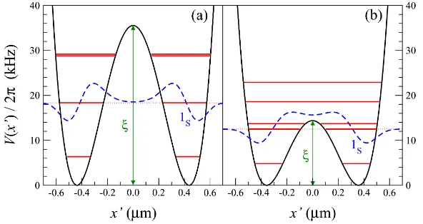
For the calculation of the trapping potential of Equation (1), we have assumed infinitely long wires of finite section 700 nm 200 nm. A trapping potential with two well separated minima, as shown in Figure 2 (a), is created
for mA, , G, and G.
The centers of the left and right wires are 1.60 mm apart. The center of the quadrupole wire is at a distance nm under the chip surface, whereas the left and right wires lie on the chip. We stress that the values for the currents, bias fields, size and distances of the wires are within current laboratory conditions.
Figure 2. Double well potentials created by the atom chip configuration shown in Figure 1. The energies of the first six eigenstates are shown as red horizontal lines. The blue dashed line represents the wavefunction of the third eigenstate labeled as because it originates from the symmetric combination of the trapped levels, also labeled as in the text. (a) Highest barrier
obtained with and . (b) Lowest barrier kHz obtained with mA and . In both cases the bias magnetic fields are equal
to and G.
The two potential minima are at a distance of 1.19 mm from the surface, and the line joining them is slightly tilted by an angle ° from the x
axis. This angle defines the new axis x' along which the dynamics will take place (see M. A. Cirone et al 7 for details). We also define a new axis y' parallel
to the chip surface and perpendicular to x'. The z axis remains unchanged. The trapping frequencies at the two minima verify , a clear indication that the trapped atoms will experience a quasi one-dimensional (1D) dynamics8. This necessary transverse confinement has already been approached
even in the early atom chip experiments with nano fabricated chips9. The
required potential smoothness10 and wire performance has been demonstrated
with semi-conductor substrate based atom chip fabrication11
.
I0= 40:89 mA ®= 70:25£10¡3 »=2¼= 14:4
I0= 42:01
B0x=¡9:90 G B0y= 50:0
1S
v= 1 jei »=2¼= 35:4 kHz
£
I0= 40:89 ®= 70:25£10¡3 B0x=¡9:90 B0y = 50:0
zQ= 400
¯'14:8
The value of the magnetic field at the two minima is G. This value minimizes the decoherence induced by fluctuations of the dc currents for the hyperfine states and of the ground state of 87
Rb 12,13
. These clock states will therefore be used to store the qubit information at the end of the gate operation. For a detailed description of the two-photon Raman process involved for the transfer of the qubit information from the internal to the external degree of freedom, we refer the reader to References 7 and 14.
2. Two-qubit p conditional phase gate
As it can be noticed in Figure 2 (a), when the barrier is high the translational wavefunctions of the atoms do not overlap in the inter-well region. In this type of environment, the atoms do not interact. On the other hand, when the barrier is lowered, as in Figure 2 (b), tunneling takes place and the probability of finding the atoms in the classically forbidden region is not negligible any more. As a consequence, the energy splitting between the symmetric and anti-symmetric state combinations increases quickly when the barrier height x is lowered. This effect is clearly selective in the sense that it affects differently the ground and excited translational states. It therefore constitutes an interesting candidate for the implementation of a conditional logical gate.
In the present scheme, the barrier height is controlled by varying simultaneously the intensities and in the quadrupole and in the perpendicular wires. In a first and simple implementation of the phase gate, we impose a linear variation of the barrier height with time. The phase gate is decomposed in three steps:
When the barrier is lowered and the double-well potential changes from the one of Figure 2 (a) to the one of Figure 2 (b).
When the inter-well barrier is fixed at its lowest value, such that a large inter-atomic interaction takes place.
Finally, when the inter-well barrier is raised again until the initial condition is recovered.
The linear variation of is obtained by changing and only, as depicted by the solid lines shown in Figure 3 (a). We have verified that this simultaneous variation of the dc currents does not modify the direction x' along which the dynamics is taking place. The value of the magnetic field at the potential minima also remains equal to 3.23 G during the whole gate operation. A quasi-adiabatic dynamics is therefore likely if ms.
Figure 3. The times , and delimit the three steps which constitute the conditional phase gate. (a) Variation of the dc current (red lines) in the quadrupole wire and of (blue lines) during the gate operation. The solid lines correspond to a simple linear gate and the dashed lines represent an optimized gate (see text for details). (b) Variation of the barrier height (green dashed line) and of the energies of the first six instantaneous eigenstates of the double well potential (solid lines) in the case of the optimized gate.
The gate operation is followed by solving the time-dependent Schrödinger equation along the double-well direction x' for the wave packet
describing the motion of the two atoms
.
(4)The two-dimensional time-dependent Hamiltonian is written as
,
(5)where denotes the kinetic energy operator along the q-coordinate. The two-dimensional potential is given by the following sum
,
(6)where is the trapping potential (3) created by the atom chip and represents the averaged interaction potential between the two atoms at time t
.
(7)T0 (T0+T1) (2T0+T1)
I0(t)
®(t) =I1(t)=I0(t) =I2(t)=I0(t)
»(t)
ª(x0
1; x02; t)
i~ @
@tª(x 0
1; x02; t) =H(x01; x02; t) ª(x01; x02; t)
H(x0
1; x02; t) = ^Tx0
1+ ^Tx02+V2D(x 0
1; x02; t) ^
Tq
V2D(x01; x02; t) =V(x01; t) +V(x02; t) +Vint(jx02¡x01j; t)
V(x0; t) Vint(jx02¡x01j; t)
This last expression is obtained by averaging the three-dimensional delta function interaction potential over the lowest trap states along the y' and z
directions15. One can note that the atom-atom interaction strength is
proportional to the s-wave scattering length . Since the orthogonal trapping frequencies and vary slightly during the gate operation8, the averaged
interaction strength is also slightly time-dependent.
We solve the time-dependent Schrödinger equation (4) in a basis set approach by propagating the initial state of the two-atom system in time. We start with the atoms initially in one of the first four eigenstates , , or of the double-well potential (6) shown in Figure 2 (a). The wavefunction
is then expanded as
,
(8)where represents the wavefunctions associated to the instantaneous eigenstates of the two-dimensional potential of Eq. (6). Inserting this expansion into the time-dependent Schrödinger equation (4) yields the following set of first order coupled ordinary differential equations for the complex coefficients
,
(9)where denotes the energy of the eigenstate and is a time-dependent non-adiabatic coupling arising from the time variation of the barrier height
.
(10)This set of equations is solved using an accurate Shampine-Gordon algorithm16
. In order to analyze the dynamics taking place during the gate operation, it is useful to examine how the energies of the two-atom translational eigenstates vary with the barrier height. These quantities are responsible for the build-up of the dynamical phases , , and , and therefore of the global conditional phase . This variation is shown in Figure 4 (a), as a function of the barrier height expressed in terms of magnetic field . During the course of the gate, the energies of the four two-qubit eigenstates vary by about 30%, while their difference , shown in Figure 4 (b), changes by four orders of magnitude. This exponential scaling is a signature of tunneling. For each barrier height, a gate duration can be extracted. This quantity is shown in Figure 4 (c), and it corresponds to the gate duration that one could achieve in a static gate implementation7. One can see from this graph
that the minimum gate duration achievable with the present parameters is about 5 ms.
Figure 4. (a) Variation of the energies , , and of the four qubit states (full black line), (dashed green line), (full red line) and (full blue line) as a function of the barrier height expressed in terms of magnetic field . (b) Variation of with the barrier height. (c) Variation of with the barrier height.
At the end of the propagation the coefficients are analyzed to calculate the infidelity of the gate
,
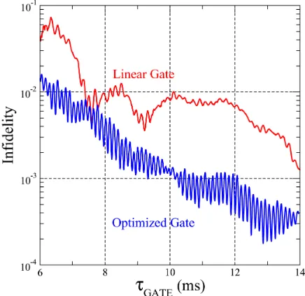
(11)where the sum runs over all possible initial qubit states. The infidelity is therefore a measure of the deviation from adiabaticity which arises from the non-adiabatic couplings . This quantity is plotted in Figure 5 (red line for the linear gate) as a function of the gate duration. It shows an oscillatory behavior partially similar to the one observed with atoms trapped in an optical lattice17. The succession of maxima and minima is a signature of constructive
and destructive interferences between two distinct pathways of excitation of the initial qubit state. Indeed the initial state may be excited in the time intervals
I= X i=jggi¢¢¢jeei
³
1¡ jci(tf)j2
´ "00 "01 "10 "11 jgei
jggi
jegi jeei
¢B ¢"="00+"11¡"01¡"10
¿gate=¼=¢"
ci(tf) (t=tf)
and , when the barrier is lowered and raised. The nature of this interference depends on the phases which develop during the gate operation17. The periodicity of the oscillation is simply related
to the Bohr frequencies associated with the energy splitting of the two-atom eigenstates. The linear gate configuration proposed here can achieve a relatively high fidelity of about 99.6% in just 7.6 ms.
Figure 5. Infidelity of the conditional phase gate as a function of the gate duration. The red and blue lines correspond to the infidelities calculated for the linear and optimized gates respectively.
One should also realize that in the general case the couplings between the initial qubit states and the other accessible two-atom eigenstates vary with time. These couplings effectively increase when the inter-well barrier approaches the energy of the initial state. The linear gate proposed until now is therefore far from being optimal for the maximization of the gate fidelity. We have thus implemented an optimized gate which tends to minimize these couplings during the whole gate duration. For this purpose, we impose a fast variation of the barrier height at early times , while this variation is much slower when . This is done by choosing
.
(12)In this expression, is a dimensionless proportionality factor, which can be
decreased to achieve larger gate durations. The first derivative with respect to time of the barrier height is therefore chosen such that the maximum effective first-order coupling between the highest energy qubit state and all other states remains constant during the whole gate duration. With this approach, higher fidelities are expected when compared to a linear gate of the same duration.
The variations of and for this optimized gate are shown as dashed lines in Figure 3 (a). Figure 5 shows that the optimized gate infidelity (blue line) is, on average, improved by a factor of about 6 when compared to the linear gate. As a consequence, this optimized gate can achieve fidelities of 99% in only 6.3 ms and of 99.9% in just 10.3 ms.
3. Conclusions
When neutral atoms are used, it is highly desirable to employ both the vibrational and the internal states as qubit states. Vibrational states are very promising in terms of gate performance, while internal states, in a carefully chosen magnetic field environment, are highly protected from decoherence12. In
addition, the readout process can be achieved efficiently with internal states using fluorescence measurement techniques. Two-photon Raman processes can be used to transfer the qubit states from one representation to the other7,14
. We have presented in this proceeding a detailed analysis of the implementation of a quantum phase gate with neutral rubidium atoms on atom chips. Our analysis is quite close to the experimental conditions and is within the reach of current technology. We have shown how to create a double well potential near the surface and studied the performance of the phase gate. We have found that a fidelity of 99.9% can be achieved in just 10.3 ms. The results presented here are a significant improvement when compared to an implementation using a static trap7
.
Finally, an important additional mechanism one has to consider in a realistic evaluation of the performance of quantum gates on atom chips, is the possibility of loss and decoherence of the qubits during the operation caused by thermal electromagnetic fields generated by the nearby, “hot” solid substrate18,19. Following the treatment of Henkel and Wilkens18, we estimate the
lifetimes for our example setup to 0.8 s, limiting the fidelity to 98.7% at a gate operation time of 9 ms. Reducing the thickness of the wires down to 50 nm and increasing the width of the central wire to 3 mm will increase the lifetime to over 3 s and increase the fidelity to 99.7% at a gate operation time of 11 ms. With an optimized wire geometry, fidelities of better than 99.9% should therefore be possible in realistic settings with present day atom chip
»(t)
jeei
technology.
Acknowledgments
M. A. Cirone, A. Negretti, T. Calarco and J. Schmiedmayer acknowledge financial support from the European Union, contract number IST-2001-38863 (ACQP). T. Calarco also acknowledges financial support from the European Union through the FP6-FET Integrated Project CT-015714 (SCALA) and a EU Marie Curie Outgoing International Fellowship, and from the National Science Foundation through a grant for the Institute for Theoretical Atomic, Molecular and Optical Physics at Harvard University and Smithsonian Astrophysical Observatory. E. Charron acknowledges the IDRIS-CNRS supercomputer center for the contract number 08/051848 and the financial support of the LRC of the CEA, under contract number DSM05-33. Laboratoire de Photophysique Moléculaire is associated to Université Paris-Sud 11. We wish to thank P. Krüger, J. Reichel and P. Treutlein for useful discussions about experimental details.
References
1. M. A. Nielsen and I. L. Chuang, Quantum Computation and Quantum Information, Cambridge University Press, Cambridge (2000).
2. P. W. Shor, Proc. 35th Annual Symposium on Foundations of Computer Science (Shafi Goldwasser, ed.), IEEE Computer Society Press (1994).
3. L. K. Grover, Phys. Rev. Lett.79, 325 (1997).
4. A. Barenco, C. H. Bennett, R. Cleve, D. P. DiVincenzo, N. Margolus, P. Shor, T. Sleator, J. A. Smolin, and H. Weinfurter Phys. Rev. A 52, 3457 (1995).
5. R. Folman, P. Krüger, J. Schmiedmayer, J. Denschlag, and C. Henkel,
Adv. At. Mol. Opt. Phys.48, 263 (2002).
6. E. A. Hinds, C. J. Vale and M. G. Boshier, Phys. Rev. Lett. 86, 1462 (2001) ; W. Hänsel, J. Reichel, P. Hommelhoff and T. W. Hänsch, Phys. Rev. A 64, 063607 (2001) ; T. Schumm, S. Hofferberth, L. M. Andersson, S. Wildermuth, S. Groth, I. Bar-Joseph, J. Schmiedmayer and P. Krüger,
Nature Physics 1, 57 (2005).
7. M. A. Cirone, A. Negretti, T. Calarco, P. Krüger, and J. Schmiedmayer,
Eur. J. Phys. D35, 165 (2005).
8. During the gate operation, the trapping frequencies vary in the ranges 13.0-10.9 kHz, 157.5-154.3 kHz and 153.8-150.9 kHz for , and respectivelly.
9. R. Folman, P. Krüger, D. Cassettari, B. Hessmo, T. Maier, and J. Schmiedmayer, Phys. Rev. Lett. 84, 4749 (2000).
10. P. Krüger, L.M. Andersson, S. Wildermuth, S. Hofferberth, E.Haller, S. Aigner, S. Groth, I. Bar-Joseph and J. Schmiedmayer, e-print arXiv: cond-mat/0504686.
11. S. Groth, P. Krüger, S. Wildermuth, R. Folman, T. Fernholz, D. Mahalu, I. Bar-Joseph, and J. Schmiedmayer, Appl. Phys. Lett.85, 2980 (2004). 12. P. Treutlein, P. Hommelhoff, T. Steinmetz, T. W. H\"ansch, and J. Reichel,
Phys. Rev. Lett.92, 203005 (2004).
13. D. M. Harber, H. J. Lewandowski, J. M. McGuirk, and E. A. Cornell,
Phys. Rev. A66, 053616 (2002).
14. E. Charron, M. A. Cirone, A. Negretti, J. Schmiedmayer and T. Calarco,
Phys. Rev. A73, in press (2006) and e-print arXiv:quant-ph/0603138
15. T. Calarco, E. A. Hinds, D. Jaksch, J. Schmiedmayer, J. I. Cirac, and P. Zoller Phys. Rev. A 61, 022304 (2000).
16. L. F. Shampine and M. Gordon, Computer solution of ordinary differential
equations: the initial value problem, W. H. Freemann and Company, San
Francisco, (1975). http://www.csit.fsu.edu/~burkardt/f_src/ode/ode.f90
17. E. Charron, E. Tiesinga, F. Mies, and C. Williams, Phys. Rev. Lett. 88, 077901 (2002).
18. C. Henkel and M. Wilkens, Europhys. Lett. 47, 414 (1999) ; C. Henkel, S. Pötting and M. Wilkens, Appl. Phys. B69, 379 (1999) ; C. Henkel and S. Pötting, Appl. Phys. B72, 73 (2001) ; C. Henkel, Eur. Phys. J. D35, 59 (2005).