Accelerometer
ADXL335
FEATURES
3-axis sensing
Small, low profile package 4 mm × 4 mm × 1.45 mm LFCSP Low power : 350 µA (typical)
Single-supply operation: 1.8 V to 3.6 V 10,000 g shock survival
Excellent temperature stability
BW adjustment with a single capacitor per axis RoHS/WEEE lead-free compliant
APPLICATIONS
Cost sensitive, low power, motion- and tilt-sensing applications
Mobile devices Gaming systems Disk drive protection Image stabilization Sports and health devices
GENERAL DESCRIPTION
The ADXL335 is a small, thin, low power, complete 3-axis accel-erometer with signal conditioned voltage outputs. The product measures acceleration with a minimum full-scale range of ±3 g.
It can measure the static acceleration of gravity in tilt-sensing applications, as well as dynamic acceleration resulting from motion, shock, or vibration.
The user selects the bandwidth of the accelerometer using the CX, CY, and CZ capacitors at the XOUT, YOUT, and ZOUT pins.
Bandwidths can be selected to suit the application, with a range of 0.5 Hz to 1600 Hz for the X and Y axes, and a range of 0.5 Hz to 550 Hz for the Z axis.
The ADXL335 is available in a small, low profile, 4 mm × 4 mm × 1.45 mm, 16-lead, plastic lead frame chip scale package (LFCSP_LQ).
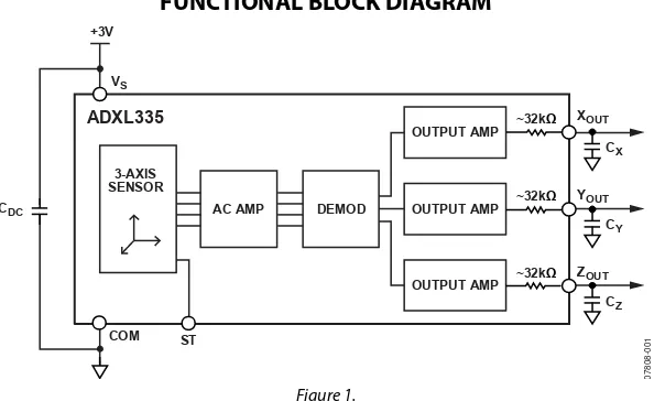
FUNCTIONAL BLOCK DIAGRAM
0
AC AMP DEMOD
OUTPUT AMP
ADXL335 ~32kΩ
~32kΩ ~32kΩ CDC
TABLE OF CONTENTS
Features ... 1
Applications ... 1
General Description ... 1
Functional Block Diagram ... 1
Revision History ... 2
Specifications ... 3
Absolute Maximum Ratings ... 4
ESD Caution ... 4
Pin Configuration and Function Descriptions ... 5
Typical Performance Characteristics ... 6
Theory of Operation ... 10
Mechanical Sensor ... 10
Performance ... 10
Applications Information ... 11
Power Supply Decoupling ... 11
Setting the Bandwidth Using CX, CY, and CZ ... 11
Self-Test ... 11
Design Trade-Offs for Selecting Filter Characteristics: The Noise/BW Trade-Off ... 11
Use with Operating Voltages Other Than 3 V ... 12
Axes of Acceleration Sensitivity ... 12
Layout and Design Recommendations ... 13
Outline Dimensions ... 14
Ordering Guide ... 14
REVISION HISTORY
1/10—Rev. A to Rev. B Changes to Figure 21 ... 97/09—Rev. 0 to Rev. A Changes to Figure 22 ... 9
Changes to Outline Dimensions ... 14
SPECIFICATIONS
TA = 25°C, VS = 3 V, CX = CY = CZ = 0.1 μF, acceleration = 0 g, unless otherwise noted. All minimum and maximum specifications are
guaranteed. Typical specifications are not guaranteed.
Table 1.
Parameter Conditions Min Typ Max Unit
SENSOR INPUT Each axis
Measurement Range ±3 ±3.6 g
Nonlinearity % of full scale ±0.3 %
Package Alignment Error ±1 Degrees
Interaxis Alignment Error ±0.1 Degrees
Cross-Axis Sensitivity1 ±1 %
SENSITIVITY (RATIOMETRIC)2 Each axis
Sensitivity at XOUT, YOUT, ZOUT VS = 3 V 270 300 330 mV/g
Sensitivity Change Due to Temperature3 V
S = 3 V ±0.01 %/°C
ZERO g BIAS LEVEL (RATIOMETRIC)
0 g Voltage at XOUT, YOUT VS = 3 V 1.35 1.5 1.65 V
0 g Voltage at ZOUT VS = 3 V 1.2 1.5 1.8 V
0 g Offset vs. Temperature ±1 mg/°C
NOISE PERFORMANCE
Noise Density XOUT, YOUT 150 μg/√Hz rms
Noise Density ZOUT 300 μg/√Hz rms
FREQUENCY RESPONSE4
Bandwidth XOUT, YOUT5 No external filter 1600 Hz
Bandwidth ZOUT5 No external filter 550 Hz
RFILT Tolerance 32 ± 15% kΩ
Sensor Resonant Frequency 5.5 kHz
SELF-TEST6
OUTPUT AMPLIFIER
Output Swing Low No load 0.1 V
Output Swing High No load 2.8 V
POWER SUPPLY
Operating Voltage Range 1.8 3.6 V
Supply Current VS = 3 V 350 μA
Turn-On Time7 No external filter 1 ms
TEMPERATURE
Operating Temperature Range −40 +85 °C
1 Defined as coupling between any two axes. 2 Sensitivity is essentially ratiometric to VS.
3 Defined as the output change from ambient-to-maximum temperature or ambient-to-minimum temperature. 4 Actual frequency response controlled by user-supplied external filter capacitors (C
X, CY, CZ).
ABSOLUTE MAXIMUM RATINGS
Table 2.
Parameter Rating
Acceleration (Any Axis, Unpowered) 10,000 g
Acceleration (Any Axis, Powered) 10,000 g
VS −0.3 V to +3.6 V
All Other Pins (COM − 0.3 V) to (VS + 0.3 V)
Output Short-Circuit Duration (Any Pin to Common)
Indefinite
Temperature Range (Powered) −55°C to +125°C
Temperature Range (Storage) −65°C to +150°C
Stresses above those listed under Absolute Maximum Ratings may cause permanent damage to the device. This is a stress rating only; functional operation of the device at these or any other conditions above those indicated in the operational section of this specification is not implied. Exposure to absolute maximum rating conditions for extended periods may affect device reliability.
PIN CONFIGURATION AND FUNCTION DESCRIPTIONS
1. EXPOSED PAD IS NOT INTERNALLY CONNECTED BUT SHOULD BE SOLDERED FOR MECHANICAL INTEGRITY.
NC = NO CONNECT (Not to Scale)
+Z
+X +Y
Figure 2. Pin Configuration
Table 3. Pin Function Descriptions
Pin No. Mnemonic Description
1 NC No Connect.1
EP Exposed Pad Not internally connected. Solder for mechanical integrity.
TYPICAL PERFORMANCE CHARACTERISTICS
N > 1000 for all typical performance plots, unless otherwise noted.
50
1.42 1.44 1.46 1.48 1.50 1.52 1.54 1.56 1.58
%
OUTPUT (V) 07
80
1.42 1.44 1.46 1.48 1.50 1.52 1.54 1.56 1.58
%
1.42 1.44 1.46 1.48 1.50 1.52 1.54 1.56 1.58
%
OUTPUT (V) 07
80
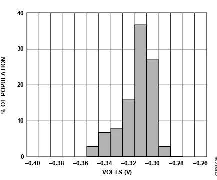
–0.40 –0.38 –0.36 –0.34 –0.32 –0.30 –0.28 –0.26
Figure 6. X-Axis Self-Test Response at 25°C, VS = 3 V
0.26 0.28 0.30 0.32 0.34 0.36 0.38 0.40
Figure 7. Y-Axis Self-Test Response at 25°C, VS = 3 V
0.48 0.50 0.52 0.54 0.56 0.58 0.60 0.62
%
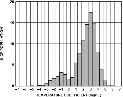
TEMPERATURE COEFFICIENT (mg/°C) 0
Figure 9. X-Axis Zero g Bias Temperature Coefficient, VS = 3 V
%
TEMPERATURE COEFFICIENT (mg/°C) 0
Figure 10. Y-Axis Zero g Bias Temperature Coefficient, VS = 3 V
%
TEMPERATURE COEFFICIENT (mg/°C) 0
Figure 11. Z-Axis Zero g Bias Temperature Coefficient, VS = 3 V
1.45
Figure 12. X-Axis Zero g Bias vs. Temperature— Eight Parts Soldered to PCB
1.45
Figure 13. Y-Axis Zero g Bias vs. Temperature— Eight Parts Soldered to PCB
1.30
%
0.285 0.288 0.291 0.294 0.297 0.300 0.303 0.306 0.309 0.312 0.315
0
0.285 0.288 0.291 0.294 0.297 0.300 0.303 0.306 0.309 0.312 0.315 25
0.285 0.288 0.291 0.294 0.297 0.300 0.303 0.306 0.309 0.312 0.315 25
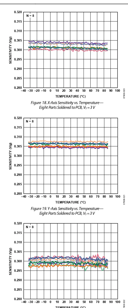
Figure 18. X-Axis Sensitivity vs. Temperature— Eight Parts Soldered to PCB, VS = 3 V
Figure 19. Y-Axis Sensitivity vs. Temperature— Eight Parts Soldered to PCB, VS = 3 V
SUPPLY (V)
CURRE
NT
(
µ
A)
0 100
50 150 200 250 300 350
1.5 2.0 2.5 3.0 3.5 4.0
0
78
08
-02
3
Figure 21. Typical Current Consumption vs. Supply Voltage
TIME (1ms/DIV) CH4: ZOUT,
500mV/DIV
CH3: YOUT,
500mV/DIV
CH1: POWER, 1V/DIV
CH2: XOUT, 500mV/DIV
OUTPUTS ARE OFFSET FOR CLARITY CX = CY = CZ = 0.0047µF
07
80
8-0
24
THEORY OF OPERATION
The ADXL335 is a complete 3-axis acceleration measurement system. The ADXL335 has a measurement range of ±3 g
mini-mum. It contains a polysilicon surface-micromachined sensor and signal conditioning circuitry to implement an open-loop acceleration measurement architecture. The output signals are analog voltages that are proportional to acceleration. The accelerometer can measure the static acceleration of gravity in tilt-sensing applications as well as dynamic acceleration resulting from motion, shock, or vibration.
The sensor is a polysilicon surface-micromachined structure built on top of a silicon wafer. Polysilicon springs suspend the structure over the surface of the wafer and provide a resistance against acceleration forces. Deflection of the structure is meas-ured using a differential capacitor that consists of independent fixed plates and plates attached to the moving mass. The fixed plates are driven by 180° out-of-phase square waves. Acceleration deflects the moving mass and unbalances the differential capacitor resulting in a sensor output whose amplitude is proportional to acceleration. Phase-sensitive demodulation techniques are then used to determine the magnitude and direction of the
acceleration.
The demodulator output is amplified and brought off-chip through a 32 kΩ resistor. The user then sets the signal bandwidth of the device by adding a capacitor. This filtering improves measurement resolution and helps prevent aliasing.
MECHANICAL SENSOR
The ADXL335 uses a single structure for sensing the X, Y, and Z axes. As a result, the three axes’ sense directions are highly orthogonal and have little cross-axis sensitivity. Mechanical misalignment of the sensor die to the package is the chief source of cross-axis sensitivity. Mechanical misalignment can, of course, be calibrated out at the system level.
PERFORMANCE
Rather than using additional temperature compensation circui-try, innovative design techniques ensure that high performance is built in to the ADXL335. As a result, there is no quantization error or nonmonotonic behavior, and temperature hysteresis is very low (typically less than 3 mg over the −25°C to +70°C
APPLICATIONS INFORMATION
POWER SUPPLY DECOUPLING
For most applications, a single 0.1 μF capacitor, CDC, placed
close to the ADXL335 supply pins adequately decouples the accelerometer from noise on the power supply. However, in applications where noise is present at the 50 kHz internal clock frequency (or any harmonic thereof), additional care in power supply bypassing is required because this noise can cause errors in acceleration measurement.
If additional decoupling is needed, a 100 Ω (or smaller) resistor or ferrite bead can be inserted in the supply line. Additionally, a larger bulk bypass capacitor (1 μF or greater) can be added in parallel to CDC. Ensure that the connection from the ADXL335
ground to the power supply ground is low impedance because noise transmitted through ground has a similar effect to noise transmitted through VS.
SETTING THE BANDWIDTH USING C
X, C
Y, AND C
ZThe ADXL335 has provisions for band limiting the XOUT, YOUT,
and ZOUT pins. Capacitors must be added at these pins to
imple-ment low-pass filtering for antialiasing and noise reduction. The equation for the 3 dB bandwidth is
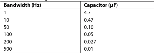
F−3 dB = 1/(2π(32 kΩ) × C(X, Y, Z))
or more simply
F–3 dB = 5 μF/C(X, Y, Z)
The tolerance of the internal resistor (RFILT) typically varies as
much as ±15% of its nominal value (32 kΩ), and the bandwidth varies accordingly. A minimum capacitance of 0.0047 μF for CX,
CY, and CZ is recommended in all cases.
Table 4. Filter Capacitor Selection, CX, CY, and CZ
Bandwidth (Hz) Capacitor (µF)
1 4.7
The ST pin controls the self-test feature. When this pin is set to VS, an electrostatic force is exerted on the accelerometer beam.
The resulting movement of the beam allows the user to test if the accelerometer is functional. The typical change in output is −1.08 g (corresponding to −325 mV) in the X-axis, +1.08 g
(or +325 mV) on the Y-axis, and +1.83 g (or +550 mV) on the
Z-axis. This ST pin can be left open-circuit or connected to
Never expose the ST pin to voltages greater than VS + 0.3 V.
If this cannot be guaranteed due to the system design (for instance, if there are multiple supply voltages), then a low VF clamping diode between ST and VS is recommended.
DESIGN TRADE-OFFS FOR SELECTING FILTER
CHARACTERISTICS: THE NOISE/BW TRADE-OFF
The selected accelerometer bandwidth ultimately determines the measurement resolution (smallest detectable acceleration). Filtering can be used to lower the noise floor to improve the resolution of the accelerometer. Resolution is dependent on the analog filter bandwidth at XOUT, YOUT, and ZOUT.The output of the ADXL335 has a typical bandwidth of greater than 500 Hz. The user must filter the signal at this point to limit aliasing errors. The analog bandwidth must be no more than half the analog-to-digital sampling frequency to minimize aliasing. The analog bandwidth can be further decreased to reduce noise and improve resolution.
The ADXL335 noise has the characteristics of white Gaussian noise, which contributes equally at all frequencies and is described in terms of μg/√Hz (the noise is proportional to the
square root of the accelerometer bandwidth). The user should limit bandwidth to the lowest frequency needed by the applica-tion to maximize the resoluapplica-tion and dynamic range of the accelerometer.
With the single-pole, roll-off characteristic, the typical noise of the ADXL335 is determined by
) 1.6
( ×
×
=NoiseDensity BW
Noise rms
It is often useful to know the peak value of the noise. Peak-to-peak noise can only be estimated by statistical methods. Table 5 is useful for estimating the probabilities of exceeding various peak values, given the rms value.
Table 5. Estimation of Peak-to-Peak Noise
Peak-to-Peak Value
% of Time That Noise Exceeds Nominal Peak-to-Peak Value
2 × rms 32
4 × rms 4.6
6 × rms 0.27
USE WITH OPERATING VOLTAGES OTHER THAN 3 V
The ADXL335 is tested and specified at VS = 3 V; however, itcan be powered with VS as low as 1.8 V or as high as 3.6 V. Note
that some performance parameters change as the supply voltage is varied.
The ADXL335 output is ratiometric, therefore, the output sensitivity (or scale factor) varies proportionally to the supply voltage. At VS = 3.6 V, the output sensitivity is typi-
cally 360 mV/g. At VS = 2 V, the output sensitivity is typically
195 mV/g.
The zero g bias output is also ratiometric, thus the zero g
output is nominally equal to VS/2 at all supply voltages.
The output noise is not ratiometric but is absolute in volts; therefore, the noise density decreases as the supply voltage increases. This is because the scale factor (mV/g) increases
while the noise voltage remains constant. At VS = 3.6 V,
the X-axis and Y-axis noise density is typically 120 μg/√Hz,
whereas at VS = 2 V, the X-axis and Y-axis noise density is
typically 270 μg/√Hz.
Self-test response in g is roughly proportional to the square of
the supply voltage. However, when ratiometricity of sensitivity is factored in with supply voltage, the self-test response in volts is roughly proportional to the cube of the supply voltage. For example, at VS = 3.6 V, the self-test response for the ADXL335
is approximately −560 mV for the X-axis, +560 mV for the Y-axis, and +950 mV for the Z-axis.
At VS = 2 V, the self-test response is approximately −96 mV for
the X-axis, +96 mV for the Y-axis, and −163 mV for the Z-axis. The supply current decreases as the supply voltage decreases. Typical current consumption at VS = 3.6 V is 375 μA, and
typi-cal current consumption at VS = 2 V is 200 μA.
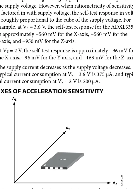
AXES OF ACCELERATION SENSITIVITY
AZ
Figure 23. Axes of Acceleration Sensitivity; Corresponding Output Voltage Increases When Accelerated Along the Sensitive Axis.
XOUT = –1g
LAYOUT AND DESIGN RECOMMENDATIONS
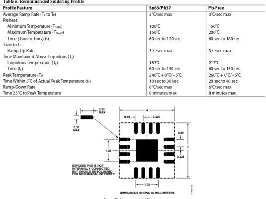
The recommended soldering profile is shown in Figure 25 followed by a description of the profile features in Table 6. The recommended PCB layout or solder land drawing is shown in Figure 26.
07
Figure 25. Recommended Soldering Profile
Table 6. Recommended Soldering Profile
Profile Feature Sn63/Pb37 Pb-Free
Average Ramp Rate (TL to TP) 3°C/sec max 3°C/sec max
Preheat
Minimum Temperature (TSMIN) 100°C 150°C
Maximum Temperature (TSMAX) 150°C 200°C
Time (TSMIN to TSMAX)(tS) 60 sec to 120 sec 60 sec to 180 sec
TSMAX to TL
Ramp-Up Rate 3°C/sec max 3°C/sec max
Time Maintained Above Liquidous (TL)
Liquidous Temperature (TL) 183°C 217°C
Time (tL) 60 sec to 150 sec 60 sec to 150 sec
Peak Temperature (TP) 240°C + 0°C/−5°C 260°C + 0°C/−5°C
Time Within 5°C of Actual Peak Temperature (tP) 10 sec to 30 sec 20 sec to 40 sec
Ramp-Down Rate 6°C/sec max 6°C/sec max
Time 25°C to Peak Temperature 6 minutes max 8 minutes max
EXPOSED PAD IS NOT INTERNALLY CONNECTED BUT SHOULD BE SOLDERED FOR MECHANICAL INTEGRITY.
OUTLINE DIMENSIONS
1.40 0.05 MAX
0.02 NOM
COMPLIANT TO JEDEC STANDARDS MO-220-WGGD.
FOR PROPER CONNECTION OF THE EXPOSED PAD, REFER TO THE PIN CONFIGURATION AND FUNCTION DESCRIPTIONS SECTION OF THIS DATA SHEET.
Figure 27. 16-Lead Lead Frame Chip Scale Package [LFCSP_LQ] 4 mm × 4 mm Body, 1.45 mm Thick Quad
(CP-16-14)
Dimensions shown in millimeters
ORDERING GUIDE
Model1 Measurement Range Specified Voltage Temperature Range Package Description Package Option
ADXL335BCPZ ±3 g 3 V −40°C to +85°C 16-Lead LFCSP_LQ CP-16-14
ADXL335BCPZ–RL ±3 g 3 V −40°C to +85°C 16-Lead LFCSP_LQ CP-16-14
ADXL335BCPZ–RL7 ±3 g 3 V −40°C to +85°C 16-Lead LFCSP_LQ CP-16-14
EVAL-ADXL335Z Evaluation Board
NOTES
Analog Devices offers specific products designated for automotive applications; please consult your local Analog Devices sales representative for details. Standard products sold by Analog Devices are not designed, intended, or approved for use in life support, implantable medical devices, transportation, nuclear, safety, or other equipment where malfunction of the product can reasonably be expected to result in personal injury, death, severe property damage, or severe environmental harm. Buyer uses or sells standard products for use in the above critical applications at Buyer's own risk and Buyer agrees to defend, indemnify, and hold harmless Analog Devices from any and all damages, claims, suits, or expenses resulting from such unintended use.