LAPORAN KERJA ELEKTRONIKA DASAR SEMICONDUCTOR I
TRANSISTOR
Disusun Oleh :
NAMA NIM
RIZKA CINDYANTIKA TIARA A. P. 0220120070
SUKHUFI DASATU IKRARNO 0220120072
MEKATRONIKA 2012 / 2013 TINGKAT 1
Politeknik Manufaktur
Astra
Jl.Gaya Motor Raya 8 Sunter II, Jakarta Utara 14330Telp. (021) 6519555, Fax. (021) 6519821
http://www.polman.astra.ac.id
Elektronika Dasar | Mekatronika Politeknik Manufaktur Astra 2
KATA PENGANTAR
Puji syukur Penulis panjatkan kehadirat Tuhan Yang Maha Esa yang telah memberikan rahmat, dan hidayah-Nya sehingga Penulis dapat menyelesaikan Laporan Kerja Elektronika Dasar tentang Semiconductor I dengan baik.
Laporan ini disusun sesuai dengan ketentuan yang diberikan. Laporan ini di awali dengan pendahuluan tentang pokok permasalahan yang akan dibahas pada bagian isi. Kemudian dilanjutkan dengan isi karangan yang membahas mengenai Semiconductor l. Dan diakhiri dengan penutup serta saran dan kesimpulan.
Laporan ini disusun guna membantu peningkatan pengetahuan maupun skill dalam teknik Elektronika Dasar baik di dunia pendidikan maupun nonpendidikan. Bersama ini penulis sampaikan terima kasih sebesar-besarnya kepada semua pihak yang telah memberikan kontribusi baik material maupun spiritual dari persiapan hingga terbentuknya laporan ini.
Meskipun penulis telah berupaya semaksimal mungkin untuk penyempurnaan laporan ini, namun tentu masih terdapat kesalahan atau kekurangan dalam laporan ini. Oleh karena itu, penulis mengharapkan saran dan kritik yang bersifat membangun guna penyempurnaan laporan ini.
Semoga laporan ini bermanfaat untuk lebih mengenal perkembangan teknik Elektronika Dasar, khususnya untuk pengenalan tentang Semiconductor.
Penulis,
Elektronika Dasar | Mekatronika Politeknik Manufaktur Astra 3 DAFTAR ISI KATA PENGANTAR 2 DAFTAR ISI 3 CHAPTER 1 THEORY 4 CHAPTER 2 INSTRUMENT 10 CHAPTER 3 PRACTICE 1 11 PRACTICE 2 17 PRACTICE 4 19 PRACTICE 5 25 PRACTICE 6 26 PRACTICE 7 29 PRACTICE 9 30 PRACTICE 10 35
Elektronika Dasar | Mekatronika Politeknik Manufaktur Astra 4
CHAPTER I
THEORY
7. 5. STUDY AND TRANSISTOR CHARACTERISTICS
7. 5.1. Basic ideas
There are two types of bipolar transistor: PNP and NPN. These types is similar to two assembled diodes. The NPN transistor is the complementary of the PNP one. This means that there are currents and tensions opposed in the action of a NPN transistor as compared to a PNP one. In figure 5. 1. 1. are the transistor symbol and the denomination of their pins. (As amnemonic rule to remember the names and symbols of each one of the transistors, the following can be useful: NPN, the arrow does not point; PNP, Points).
Figure 5. 1. 1.
7. 5. 1. 1. In Common Base Configuration
The moment when the direct polarization is applied to the emitter diode, the emitter electrons have not entered the base region. If VEB is bigger than 0.7
V(silicon transistor), many emitter electrons enter in such region. A few of these are diverted through the base, and most of them(>95%) are pushed through the field of the depletion layer towards the collector.
Gain αD.C.
In the previous assembly in direct polarization, the collector current almost the same as the emitter. The gain value (Gain αD.C. indicates the relation between them) is:
Elektronika Dasar | Mekatronika Politeknik Manufaktur Astra 5
αCC =
This value can be approximated to the unit in most of the analysis. 7. 5. 1. 2. Common emitter configuration
The free electrons move just as before and the emitter is full of these electrons. When VBE is bigger than 0.7 V, the emitter injects them into the base. As
the collector diode is inversely polarized, the field of the depletion cap pushes the electrons towards the collector region, from where they leave up to the external voltage source.
Figure 5. 1. 2. Gain βD.C.
This gain can be put as:
βCC =
This value is usually found between 50 and 300, though it can reach up to 1000. In the system of H-parameters analysis, hFE is used, but it is the same parameter.
7. 5. 1. 3. Relationship between αD.C. and βD.C.
With the help of Kirchoff’s laws and simple operations a simple relation between both of them can be obtained:
IE = IB + IC
= +
Elektronika Dasar | Mekatronika Politeknik Manufaktur Astra 6
βCC =
7. 5. 2. Transistor Characteristic
A way to see how a transistor operates is through graphics, which indicate the transistor voltage and current. These curves I-V will be more complex than the diode curve that has been studied due to base current effect, that has to be included.
7. 5. 2. 1. Collector curves
We can obtain information for the collector curves layout in the Common
Emitter configuration making a circuit as it is indicated in figue 5. 2. 1a. The idea is
to change the sources VBB and VDC to obtain different voltage and current in the
transistor. The usual procedure is to establish a value of IB maintaining it fixed
while VDC is varied. Measuring ID.C. and VCE+ we can get information for the
graphics IC versus VCE. For example, supposing that IB is adjusted to 10μA in
figure 5.2.1.a, immediately VD.C. is varied and the results from IC and VCE are
measured. Next, the provided data are sketched in figure 5.2.1b, which is a representation of the transistor operation. When VCE is zero, the collector diode is
not inversely polarized, and therefore, the collector current is increased in a high slop and then it is maintened almost constant. This is connected with the idea of inverse polarization of the collector diode. The inverse polarization of this diode takes approximately 0.7; and once it has reached this level,the collector gathers all the electrons which come to its depletion layer.
Elektronika Dasar | Mekatronika Politeknik Manufaktur Astra 7
Figure 5. 2. 1
Above the elbow, the exact value of VCE is not so important because the slop
of these curves is very small. The collector current does not increase considerably when the VCE voltage varies. Having the transistor a βCC of approximately 100, the
collector current is almost 100 times the base current.
Figure 5. 2. 2
If the VCE is increased too much, the collector diode passes to breakdown and the
normal action of the transistor is lost. Then the transistor stops workingas a current source. The maximum of voltage, in a transistor, is the voltage interval of the collector-emitter on which the transistor works as a current source. In figure 5.2.1b, this voltage interval VCE is between 1 V and the breakdown voltage.
Maintain the transistor in this active region and it will operate as controlled current source. If it is maintained out of this interval, the normal action of the transitor is lost.
If measurements of IC and VCE are made for IB = 20 μA, the graphics layout
can be done as it is indicated in figure 5. 2. 1c. The curves are similar, except that above the elbow, the collector current is approximately equal to 2mA.
If several curves for different IB are put together and drawn in the same
graphics, we obtain collector curves as the ones indicated in figure 5. 2. 2. As we have been using a transistor with a βDC of approximately 100, the collector current
is nearly 100 times greater than the base current for any point from the active region. These curves are usually called collector static curves, because the D.C. voltage and current values are down.
Elektronika Dasar | Mekatronika Politeknik Manufaktur Astra 8
7. 5. 2. 2. Base curves
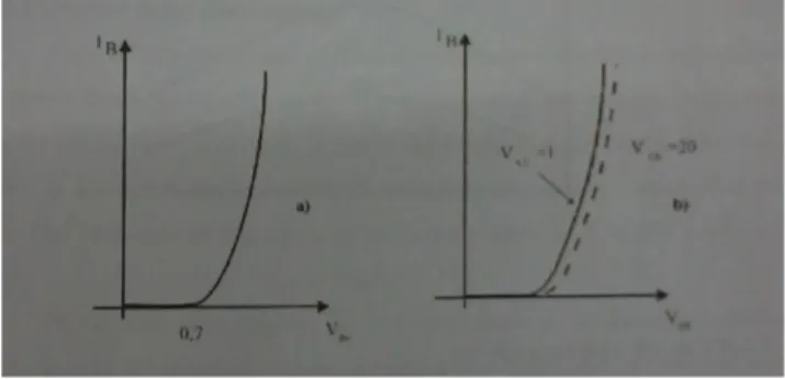
Figure 5. 2. 3a shows a base current graphics against the base-emitter voltage. As the base-emitter section of a transistor is a diode, we would expect to see the graphics similar to a diode curve, which is almost what is obtained. We must remember that there are more variables in a transistor than in a diode.
A high collector voltage makes this get some more electrons, something that decrease the base current. This idea is shown in figure 5.2.3b. The curve with the highest VCE has slightly less base current for a given VBE. This phenomenom called
Early effect, is underestimated.
Figure 5.2.3 7. 5. 2. 3. Current gain curves
The βD.C. from a transistor, also called current gain, change enormously.
Figure 4.7 shows a typical variation in βD.C. At a constant temperature, βD.C. increases to a maximum value when the collector current is increased; for aditonal increasesin IC, βD.C. decreases. The variation in βD.C. can be up to 3:1 on the transistor usual current range; this depends on the type of transistor.
A change in the environment temperature has some effects on βD.C. As it is indicated in figure 5.2.4, at a given collector current, an increment in the temperature will increase βD.C.. On a large temperature change significantly, βD.C. can vary in a proportion of 9:1. It must be remembered, because any design in which an exact value of βD.C. is required, is condemned to failure from the beginning.
Elektronika Dasar | Mekatronika Politeknik Manufaktur Astra 9
Figure 5.2.4 7. 5. 2. 4. Cut off and breakdown
In the collector curves in figure 5.2.2, the inferior curve belongs to the base current equal to zero. The condition IB = O is equivalent to having an open base
terminal. The current, which flows through the collector when the base is open, is called ICEO, where the CEO subscripst indicates collector to emitter with an open
base.
Figure 5.2.5
Figure 5.2.5 shows the curve IB = 0. With a collector voltge big enough, the
break voltage referred as BVCEO is reached where the subscript indicates, again, collector to emitter with open base. For a transistor normal operation, we have to maintain VCE smaller than BVCEO.
7. 5. 2. 5. Collector saturation voltage
The initial part of the curve is called saturation region, which takes in all curves between the origin and the elbow. The flat part of the curve is the active region, which the transistor operates as a controlled source of current. The final part of the curve is the break region. This region must be always avoided.
In the saturation region, the collector diode is in direct polarization, the normal action of the transistor is lost and works as a small ohmmic resistor instead of a current source. An additional increase in the base current can not produce an additional increase in the collector current. The collector-emitter voltage, in the saturation region, is generally of a few tenths of volt, depending on the quantity of the existing collector current.
Elektronika Dasar | Mekatronika Politeknik Manufaktur Astra 10
Figure 5.2.6
The collector diode must be inversely polarized so the transistor operate in the active region; this requires a tension above 1 volt, approximately.
7. 5. 2. 6. Transistor specification
The transistor of the small signal can dissipate half watt or less; the power ones , more than half watt.
VCEO indicate the collector to emitter voltage with the base open.
VCBO is the voltage between the collector and the base with the emitter
open.
VEBO is the voltage of the emitter to the base with the collector open.
IC is the nominal maximum current of DC of the collector.
PD is the maximum nominal power of the device.
The power dissipation of the transistor can be calculated by: PD = VCE.IC
7. 5. 3. Lines with DC load
A load line can be drawn in the collector curves to have more information about the transistor operation and of the region where it works. The procedure to do it is similar to the one used with the diode. In the figure 5.3.1a, the applied voltage VD.C. polarizes inversely the collector through RC. The voltage applied to
tis resistor is VDC-VEC. Therefore, the current through it is equal to
IC =
Elektronika Dasar | Mekatronika Politeknik Manufaktur Astra 11
Figure 5.3.1 7. 5. 3. 2. Cut off and saturation point
The point where the load line cuts IB = 0 is known as the cut off point.
At this point, the base current is zero and the one from the collector is extremely small. At the cut-off point, the emitter diode has come out of direct polarization and the transistor nrmal operation has been lost. With a good approximation, the collector-emitter voltage is equal to the lower extreme of the load line:
VCE(Ccorte) ≈ VCC
The interxection of the load line and the curve for IB = IB(sat) is called
saturation. At this point, the base current is equal to IB(sat), and the current that
flows through the collector is maximal. In saturation, the collector diode comes out of inverse polarization and the transistor normal action is lost again. With a good approximation, the collector current in saturation is equal to upper extreme of the load line:
IC ≈
7. 5. 3. 3. Maximum variation
The load line of D.C. indicates a transistor has a maximum output speed(limit of active voltage VCE). In figure 5.3.1b, the transistor has a maximum
output of approximately 0 to VCC. In other words, the transistor works as a
currentsource throughout the D.C. load line trajectory, exluding the saturation or cut-off points, where the current source action is lost.
7. 6. TRANSISTOR CHARACTERISTICS OPERATING AS A SWITCH
7. 6. 1. The NPN transistor as a switch
Transistor must work in the saturation or cut off point and nowhere else on the trajectory of the load line. When a transistor is saturated, it works as a closed
Elektronika Dasar | Mekatronika Politeknik Manufaktur Astra 12
switch between the collector and the emitter. when a transistor is in cut off, it works as an switch.
7. 6. 1. 1. Base current
Figure 6.1.1. shows the circuit we have analyzed up to now. Adding the voltages around the input we obtain:
IBRB + VBE – VBB = 0
IB =
Figure 6.1.1
If the base current is bigger than or equal to IB(sat), the operation point Q is
in the upper part of the load line(figure 6.1.2). In this case, the transistor works as a closed switch. However, if the base current is zero, the transistor operates in the lower part of the load line and works as an open switch.
Elektronika Dasar | Mekatronika Politeknik Manufaktur Astra 13
7. 6. 2. The PNP transistor as a switch
Figure 6.2.1
When the applied voltage to the input is next to Vdc, the transistor is in cut
off state and it does not conduct. However, when we connect a substantially lower voltage to the input, the transistor comes into saturation and closes the circuit, and with that the load 1 KΩ would have at its terminals a voltage next to VDC.
As we can see, while this circuit conducts when the base resistor of the transistor is connected “a voltage valley”, the previous one did it when it was connected to a “peak”.
7.7. COMMON EMITTER AMPLIFIER 7. 7. 1. Transistor polarization
The general operation of the transistor is in linear circuits. One example of this is the amplifiers, circuits, which increase the amplitude of an alternating input signal.
Before the alternating signal could be applied to the transistor, it should be established an operating point of the transistor. So that the circuit is maintained linear, the current and voltage fluctuations should not pass the transistor to the saturation or cut off region.
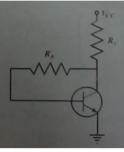
7. 7. 1. 1. Base polarization
This polarization is used in digital circuits, where it is used in cut off and saturation. It should not be used for linear circuits.
Elektronika Dasar | Mekatronika Politeknik Manufaktur Astra 14
The circuit in figure 7.1.1 shows this type of bias, where the source is the same as the one of the collector.
Figure 7.1.1
7. 7. 1. 2. Emitter feedback polarization
This circuit shown in figure 7.1.2. The idea is to try to use the voltage between the transistor terminals to compensate the βCC changes. For example, if
βCC increases, the collector current increases and increases the emitter voltage. The
base voltage and its current decrease. The reduced base current gives as a result a smaller current in the collector, which balances the original increase in βCC partly.
Elektronika Dasar | Mekatronika Politeknik Manufaktur Astra 15
7. 7. 1. 3. Collector feedback polarization
Figure 7.1.3 shows this configuration, also called auto-polarization.
Figure 7.1.3
If the temperature increases, causing the increase of βCC, more collector
current is produced. If this increases, the emitter-collector voltage decreases. This causes the voltage between terminals of the base resistor decreases and consequently the current in it decreases. The smallest base current compensates the original increment in the collector current.
7. 7. 1. 4. Voltage divider polarization This is the most used polarization.
Elektronika Dasar | Mekatronika Politeknik Manufaktur Astra 16
If we suppose that the base terminal in figure 7.1.4 is opened, we will see a voltage divider(figure 7.1.5).
VTH =
The original circuit is simplified to the two ones in figure 7.1.5 and the transistor work as a controlled current source. Due to the fact that the emitter is adapted to the base.
IE =
The collector current is approximately equal to this value.
Figure 7.1.5
It must be noticed that βCC does not appear in the emitter current formula,
which means that the circuit remains protected against variations from this parameter.
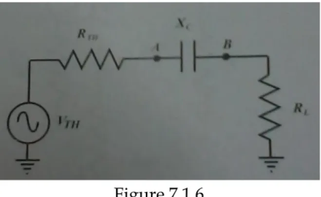
7. 7. 1. 5. Coupling capacitor
A coupling capacitor permits the step of an alternating signal from one point to another. In figure 7.1.6, the voltage in point A is transmitted to point B. If the source VTH was direct, there would not be current in the circuit, since the
Elektronika Dasar | Mekatronika Politeknik Manufaktur Astra 17
Figure 7.1.6
To transmit the A.C. voltage, the capacitative reactance XC has to be very
small compared with the resistors in series. As you will remember from the basic circuit’s theory, the magnitude of the alternating current in a RC circuit of a mesh is equal to:
I = √ 7. 7. 1. 6. By pass capacitor
A bypass capacitor is similar to a coupling capacitor, with the exception that it connects to ground one point that initially it is not connected to ground as figure 7.1.7 indicates. Point A is in short circuit to ground for an alternating signal, but it is not for D.C. one.
Figure 7.1.7 7. 7. 1. 7. Gain βca
Figure 7.1.8 shows a characteristic IC graphics in function IB. βCC is the DC
collector current ratio, IC, to the DC base current(IB). The gain βca is usually called
β. β =
Elektronika Dasar | Mekatronika Politeknik Manufaktur Astra 18
β =
Figure 7.1.8
7. 7. 2. Introduction the amplification with transistors 7. 7. 2. 1. Common emitter NPN and PNP amplifier
The idea is basically the same as with the other transistor model. Now, all the voltages and currents are inverted.
The PNP transistor is called NPN complementary. Each NPN circuit has a complementary PNP. To find this circuit:
1. The NPN transistor is replaced by another PNP one. 2. All the voltage and current are inverted
Thus, the common emitter amplifying basic circuit is the one shown in figure 7.2.1.
Figure 7.2.1
The voltage gain in circuit as the one in figure 7.2.1, where there is no bypass capacitor, is:
Elektronika Dasar | Mekatronika Politeknik Manufaktur Astra 19
CHAPTER 2
INSTRUMENT
In this practice we have used some instruments, there’re:
Jumper.
Multimeter.
Elektronika Dasar | Mekatronika Politeknik Manufaktur Astra 20
Function Generator.
Oscilloscope .
The board of Edibon C, B, E, M3 Semiconductor I.
Modul Semiconductor I.
Elektronika Dasar | Mekatronika Politeknik Manufaktur Astra 21
CHAPTER 3
PRACTICE
Practice 12 : Study of the transistor Goal :
- To analyze the bipolar transistor operation.
- To make basic study of the construction and movement of electrons and hole details.
Instrument :
- The board of Edibon C,B,E M3 Semiconductor I. - Multitester / Multimeter.
- Power Supply. - Jumper.
Figure 5.4.2 Steps :
Elektronika Dasar | Mekatronika Politeknik Manufaktur Astra 22
1. Prepare all instrument that you need. 2. Feed the board with PSU.
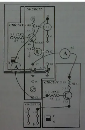
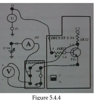
3. Connect the CIRCUIT 5 transistor with the SOURCES circuit such as shown in figure 5.4.2.
4. Take the positive connecting lead of an ammeter to the source f1 (variable 2V) and the negative one to point 5.1.
5. Take the positive connecting lead of the other ammeter to the source (variable 12V) to point 5.2.
6. Connect the point 5.3 to ground (channel Ca2) with a lead.
7. Set the ammeter A1 to measure current to the order of μA, and the A2 to the order of mA.
8. Set the source f1 in the minimum possible voltage turning the potentiometer, which is next to the source U. set f3 until the voltage attaching the collector resistor will be about 6v turning completely to the left the potentiometer, which is in the independent power supply.
9. Measure and fill it in table 5.4.1 then answer the questions. The result of 5.4.1
Base Current (μA) Collector Current (mA) βсс Gain (mA)
2.5 0.75 0.30 5 1.25 0.25 7.5 2.5 0.33 10 3.25 0.325 12.5 4.00 0.32 15 4.75 0.32 17.5 5.75 0.33 20 6.50 0.325 25 8.00 0.32 30 9.00 0.30 Table 5.4.1
C4.1. What is the collector current value when the base one is 10 μA ?
Answer : 3.25 mA
C4.2. Which graph is the correct when is done Ic currents versus Iв ?
Elektronika Dasar | Mekatronika Politeknik Manufaktur Astra 23
B. D.
C4.3. What is the βcc gain value for Iв = 5 μA ?
Answer : 250
C4.4. Without measuring, What is the approximate value of the αcc gain ?
Answer : 0.9973
Figure 5.4.4 Steps :
1. Connect the variable source of 12V (with help of the ammeter) directly with the transistor collector.
2. Set the potentiometers of f1 and f3 voltages in order to have the minimum voltage.
3. Set connecting lead from f1 to 5.1.
4. Set the multimeter to measure maximum voltage of 10V.
5. Set the negative connecting lead of the multimeter in the circuit groundand the positive one in point 5.5.
6. Measure and fill it in table 5.4.2 then answer the questions. The result of table 5.4.2
VCE = 1V VCE = 3V VCE = 6V VCE = 8V
Iв = 10 μA 15 μA 24 μA 42.5 μA 50 μA
Elektronika Dasar | Mekatronika Politeknik Manufaktur Astra 24
Iв = 30 μA 34 μA 43.5 μA 50 μA 57.5 μA
Iв = 40 μA 44.5 μA 50 μA 60 μA 62.5 μA
Iв = 50 μA 50 μA 62.5 μA 62.5 μA 67.5 μA
C4.5. Which is the collector current measured value when Iв = 30μA and VCE =
3V?
Answer : 43.5 μA
C4.6. Which is the collector current measured value when Iв = 50μA and VCE =
6V?
Answer : 62.5 μA
Graphics of Figure 5.4.5
Practice 13 : Fault study in the transitor Goal :
- To analyze the bipolar transistor operation in Fault position. Steps :
1. Feed the board with PSU.
2. Set the fault switch in circuit 5 in fault position (F) 3. Use the multimeter to measure resistances.
4. Measure and answer the questions.
0 50 100 150 200 250 300 350 1 3 6 8 50 40 30 20 10
Elektronika Dasar | Mekatronika Politeknik Manufaktur Astra 25
C4.8. What have you noticed?
A. Resistor R7 has a value too high. B. Βcc gain has a value too high.
C. The transistor is assembled in a wrong way. D. The base currents does not affected the transistor.
Practice 15 : Study of transistor as a switch Goal :
- To analyze the transistor operation as a switch. Instrument :
- The board of Edibon C,B,E M3 Semiconductor I. - Multitester / Multimeter.
- Power Supply. - Jumper.
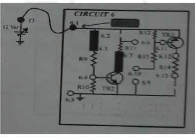
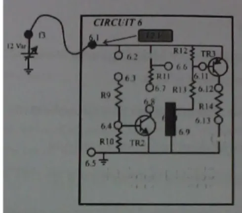
Figure 6.3.2 Steps :
1. Adjust the source f3 voltage to 12V with the base unit M-3 potentiometer. 2. Take a connecting lead from the source f3 (12V variable) to point 6.1 3. Set a link between points 6.2 and 6.3
4. Set a link between points 6.7 and 6.8
5. Measure and answer the questions C5.1. and C5.2.
Elektronika Dasar | Mekatronika Politeknik Manufaktur Astra 26
7. Remove the bridge 6.2 – 6.3 and set an ammeter between them. 8. Measure and answer the question C5.3.
9. Set again the link between 6.2 and 6.3.
10. Remove the jumper which joined 6.7 and 6.8 and set ammeter between them.
11. Measure and answer the question C5.4 until C5.7. C5.1. The transistor is operating in
A. Cut off B. Saturation
C. The lowest part of the load line D. The highest part of the load line
C5.2. What happens if the bridge 6.2 – 6.3 is removed ? A. The diode does not light
B. The diode lights
C. The diode lights intermittently
D. The diode lights shines if the source f3 voltage is decreased C5.3. Which is the base current value?
Answer : 0,6 mA
C5.4. Which is the current that we measure in this way? A. Ic
B. IE
C. Ic-IB
D. Ic+IE
C5.5. Which is the collector current value?
Answer : 0,30 mA
C5.6. Which is the voltage value of the Collector-Emitter? A. 0.7 V
B. 2V
C. 10V approximately D. 0V approximately
Elektronika Dasar | Mekatronika Politeknik Manufaktur Astra 27
Answer : 0,5 mA
Figure 6.3.3 Steps :
1. Feed the board with PSU.
2. Adjust the source f3 voltage to 12V with the base unit M-3 potentiometer. 3. Take a connecting lead from the source f3 (12V variable) to point 6.1 4. Set a link between point 6.9 and 6.10
5. Measure and answer the question C5.8.
6. Set ammeter to measure current of around 50mA.
7. Remove the link that joins points 6.9 and 6.10 and set an ammeter between them.
8. Measure and answer the question C5.9.
C5.8. What is the applied voltage to the base resistor when the transistor conducts between Collector and Emitter?
Answer : The diode lights. Its mean the TR3 operating in Saturation. C5.9. Which is the base current value?
Elektronika Dasar | Mekatronika Politeknik Manufaktur Astra 28
Figure 6.3.4 Steps :
1. Adjust the source f3 voltage to 12V with the base unit M-3 or with an independent power supply.
2. Take a connecting lead from the source f3 (12V variable) to point 6.1 3. Set a link between points 6.8 and 6.10
4. Set a connecting lead from 6.3 to 6.12
5. Set a connecting lead with an extreme connected to ground point (point 6.5 for example) and let the other extreme free, but with caution, it should not touch any point on the board.
6. Measure and answer the questions.
C5.10. Which is the resistor that fed the resistor of the PNP transistor (TR3)? A. R9
B. R10 C. R12 D. R13
Practice 17 : Study of the common emitter NPN amplifier Goal :
- To Instrument :
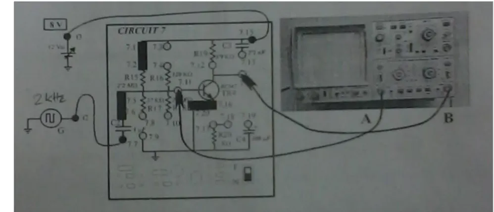
Elektronika Dasar | Mekatronika Politeknik Manufaktur Astra 29 - Multitester / Multimeter. - Power Supply. - Signal Generator. - Oscilloscope. - Jumper. Figure 7.3.2 Steps:
1. Connect the signal generator to G and GND sockets in the board. Give a sinusoidal voltage about 30 mV peak to peak.
2. Feed the board with PSU.
3. Adjust the voltage of the f3 to obtain 8V via voltmeter. 4. Set a connecting lead from f3 to point 7.15
5. Set a link between points 7.16 and 7.20
6. Measure then answer the questions and fill the table 7.3.1 C6.1. What is this polarization type?
A. A base one
B. By emitter feedback C. By collector feedback D. By voltage divider
Elektronika Dasar | Mekatronika Politeknik Manufaktur Astra 30
Table 7.3.1
Collector Base Emmiter
4,7 V ∞ V 0 V
C6.2. Which is the value of the collector voltage at this point?
Answer : 4,7 V
Figure 7.3.3 Steps:
1. Set the signal generator in sinusoidal wave of 1Hz frequency and the minimum amplitude.
2. Set the oscilloscope to two channels, set the time base is 1ms/div, the trigger in AC, alternating voltage display in AC, channel A gain is 50mV/div and channel B gain is 1V/div.
3. Increase the input signal amplitude until its voltage is 50mVpp. 4. Measure and answer the question C6.3.
5. Keep on increasing the input voltage until the output wave begin to be distorted then measure and answer the question C6.4.
6. Measure again the direct voltage in the collector with a voltmeter, just for check that it has been no change.
7. See the total voltages in the oscilloscope in DC signal. Measure and answer the question C6.5.
Elektronika Dasar | Mekatronika Politeknik Manufaktur Astra 31
C6.3. Which is the output voltage between peaks when the input is 50mVpp?
Answer : 4.4 Vpp
C6.4. What is the approximate value of the maximum input voltage at which is not distorted by the amplifier?
Answer : 0.5 Vpp
C6.5. What is the voltage gain value in this amplifier?
Answer : 88
Figure 7.3.5 Steps:
1. Assemble the circuit in figure 7.3.5
2. Analyze an amplifier with polarization through voltage division 3. Measure the voltage in the transistor and fill the table 7.3.2
C6.6. By using the formula that we have seen in the theoritical introduction, calculate the direct voltage introduced in the base through the voltage divider. Which is its value?
Answer : 1,47 V
Table 7.3.2
Collector Base Emitter
Elektronika Dasar | Mekatronika Politeknik Manufaktur Astra 32
C6.7. What is the voltage between base and emitter?
Answer : 0,675 V
C6.8. What is the value of the maximum input voltage that is not disorted by the amplifier?
Answer : 1,8 Vpp
C6.9. Which is the value of voltage gain?
Answer : 3,4
Practice 18 : Fault study in the amplifier circuit Goal :
- Instrument :
- The board of Edibon C,B,E M3 Semiconductor I. - Multitester / Multimeter.
- Power Supply. - Jumper.
Steps :
1. Maintain the last assembly made. (figure 7.3.5) 2. Set the fault switch in fault position (F)
3. Connect the voltage from power supply again. 4. Measure and answer the questions.
C6.11. What have you seen?
A. Resistor R19 is short-circuited. B. Resistor R20 is short-circuited.
C. The transistor is assemble in a wrong way. D. Capacitor C4 is switched off.
Elektronika Dasar | Mekatronika Politeknik Manufaktur Astra 33
Practice 19 : Study of the common emmiter PNP amplifier Goal :
- To Instrument :
- The board of Edibon C,B,E M3 Semiconductor I. - Multitester / Multimeter. - Power Supply. - Jumper. - Signal Generator. - Oscilloscope. Figure 7.5.2 Steps:
1. Connect the signal generator to G and GND socket. 2. Adjust the voltage giving f4 about -8V with voltmeter.
3. Set a connecting lead from the Source circuit (point f4) to Circuit 8 (Point 8.3).
4. Set a connecting lead from f3 to point 8.1
5. Measure and fill the table 7.5.1 then answer the questions.
6. For question C6.14, set display of output wave in the oscilloscope with a sinusoidal signal and it voltage is 1 Vpp input.
Elektronika Dasar | Mekatronika Politeknik Manufaktur Astra 34
Table 7.5.1
Collector Base Emitter
-2.4 V -1.45 V -1 V
C6.12. What is the voltage in the base?
Answer : -1.45 Volt
C6.13. What is the VBE voltage?
Answer : -0.55 Volt
C6.14. Which is the voltage gain?