No. Dok. : F-PBM-16 Tgl. Berlaku : 13 Desember 2010 No. Rev. : 00
KEMENTERIAN PENDIDIKAN DAN KEBUDAYAAN
POLITEKNIK NEGERI SRIWIJAYA
Jalan Srijaya Negara, Palembang 30139 Telp. 0711-353414 Fax. 0711-355918
Website :www.polisriwijaya.ac.id E-mail :[email protected]
KESEPAKATAN BIMBINGAN LAPORAN AKHIR (LA)
Kami yang bertanda tangan di bawah ini, Pihak Pertama
Nama : Khiarul Arham
NIM : 061330330278
Jurusan : Teknik Elektro
Program Studi : Teknik Telekomunikasi
Pihak Kedua
Nama : Nasron, S.T., M.T.
NIP : 196808221993031001
Jurusan : Teknik Elektro
Program Studi : Teknik Telekomunikasi
Pada hari ini ………... tanggal ……... telah sepakat untuk melakukan konsultasi bimbingan Laporan Akhir.
Konsultasi bimbingan sekurang-kurangnya 1 (satu) kali dalam satu minggu. Pelaksanaan bimbingan pada setiap hari ……… pukul ………….., tempat di Politeknik Negeri Sriwijaya.
Demikianlah kesepakatan ini dibuat dengan penuh kesadaran guna kelancaran penyelesaian Laporan Akhir.
Palembang, …....………
Pihak Pertama, Pihak Kedua,
(Khiarul Arham) (Nasron, S.T., M.T.)
NIM 061330330278 NIP 196808221993031001
Mengetahui, Ketua Jurusan
No. Dok. : F-PBM-16 Tgl. Berlaku : 13 Desember 2010 No. Rev. : 00
KEMENTERIAN PENDIDIKAN DAN KEBUDAYAAN
POLITEKNIK NEGERI SRIWIJAYA
Jalan Srijaya Negara, Palembang 30139 Telp. 0711-353414 Fax. 0711-355918
Website :www.polisriwijaya.ac.id E-mail :[email protected]
KESEPAKATAN BIMBINGAN LAPORAN AKHIR (LA)
Kami yang bertanda tangan di bawah ini, Pihak Pertama
Nama : Khiarul Arham
NIM : 061330330278
Jurusan : Teknik Elektro
Program Studi : Teknik Telekomunikasi
Pihak Kedua
Nama : Sopian Soim, S.T., M.T.
NIP : 197103142001121001
Jurusan : Teknik Elektro
Program Studi : Teknik Telekomunikasi
Pada hari ini ………... tanggal ……... telah sepakat untuk melakukan konsultasi bimbingan Laporan Akhir.
Konsultasi bimbingan sekurang-kurangnya 1 (satu) kali dalam satu minggu. Pelaksanaan bimbingan pada setiap hari ……… pukul ………….., tempat di Politeknik Negeri Sriwijaya.
Demikianlah kesepakatan ini dibuat dengan penuh kesadaran guna kelancaran penyelesaian Laporan Akhir.
Palembang, …....………
Pihak Pertama, Pihak Kedua,
(Khiarul Arham) (Sopian Soim, S.T., M.T.)
NIM 061330330278 NIP 197103142001121001
Mengetahui, Ketua Jurusan
No. Dok. : F-PBM-17 Tgl. Berlaku : 13 Desember 2010 No. Rev. : 00
KEMENTERIAN PENDIDIKAN DAN KEBUDAYAAN
POLITEKNIK NEGERI SRIWIJAYA
Jalan Srijaya Negara, Palembang 30139 Telp. 0711-353414 Fax. 0711-355918
Website :www.polisriwijaya.ac.id E-mail :[email protected]
LEMBAR BIMBINGAN LAPORAN AKHIR
Lembar : 1
Nama : Khiarul Arham
NIM : 061330330278
Jurusan/Program Studi : Teknik Elektro / Teknik Telekomunikasi
Judul Laporan Akhir : Sistem Kecerdasan Navigasi PadaWall FollowerPemadam Api Beroda dengan AlgoritmaFuzzydanEnvironment Mapping
Pembimbing I : Nasron, S.T., M.T.
No. Tanggal Uraian Bimbingan Tanda Tangan
Pembimbing
1.
2.
3.
4.
5.
6.
7.
No. Dok. : F-PBM-17 Tgl. Berlaku : 13 Desember 2010 No. Rev. : 00
No. Tanggal Uraian Bimbingan Tanda Tangan
Pembimbing
8.
9.
10.
11.
12.
Palembang, ………..
Ketua Program Studi,
(Ciksadan, S.T., M.Kom) NIP 196809071993031003 Catatan:
*) melingkari angka yang sesuai.
Ketua Jurusan/Ketua Program Studi harus memeriksa jumlah pelaksanaan bimbingan sesuai yang dipersyaratkan dalam Pedoman Laporan Akhir sebelum menandatangani lembar bimbingan ini.
No. Dok. : F-PBM-17 Tgl. Berlaku : 13 Desember 2010 No. Rev. : 00
KEMENTERIAN PENDIDIKAN DAN KEBUDAYAAN
POLITEKNIK NEGERI SRIWIJAYA
Jalan Srijaya Negara, Palembang 30139 Telp. 0711-353414 Fax. 0711-355918
Website :www.polisriwijaya.ac.id E-mail :[email protected]
LEMBAR BIMBINGAN LAPORAN AKHIR
Lembar : 1
Nama : Khiarul Arham
NIM : 061330330278
Jurusan/Program Studi : Teknik Elektro / Teknik Telekomunikasi
Judul Laporan Akhir : Sistem Kecerdasan Navigasi PadaWall FollowerPemadam Api Beroda dengan AlgoritmaFuzzydanEnvironment Mapping
Pembimbing I : Sopian Soim, S.T., M.T.
No. Tanggal Uraian Bimbingan Tanda Tangan
Pembimbing
1.
2.
3.
4.
5.
6.
7.
No. Dok. : F-PBM-17 Tgl. Berlaku : 13 Desember 2010 No. Rev. : 00
No. Tanggal Uraian Bimbingan Tanda Tangan
Pembimbing
8.
9.
10.
11.
12.
Palembang, ………..
Ketua Program Studi,
(Ciksadan, S.T., M.Kom) NIP 196809071993031003 Catatan:
*) melingkari angka yang sesuai.
Ketua Jurusan/Ketua Program Studi harus memeriksa jumlah pelaksanaan bimbingan sesuai yang dipersyaratkan dalam Pedoman Laporan Akhir sebelum menandatangani lembar bimbingan ini.
No. Dok. : F-PBM-18 Tgl. Berlaku : 13 Desember 2010 No. Rev. : 00 KEMENTERIAN PENDIDIKAN DAN KEBUDAYAAN
POLITEKNIK NEGERI SRIWIJAYA
Jalan Srijaya Negara, Palembang 30139 Telp. 0711-353414 fax. 0711-355918
Website :www.polisriwijaya.ac.id E-mail :[email protected]
REKOMENDASI UJIAN LAPORAN AKHIR (LA)
Pembimbing Laporan Akhir memberikan rekomendasi kepada,
Nama : Khiarul Arham
NIM : 061330330278
Jurusan/Program Studi : Teknik Elektro / Teknik Telekomunikasi
Judul Laporan Akhir : Sistem Kecerdasan Navigasi Pada
Wall FollowerPemadam Api Beroda dengan AlgoritmaFuzzydan
Environment Mapping
Mahasiswa tersebut telah memenuhi persyaratan dan dapat mengikuti Ujian
Laporan Akhir (LA) pada Tahun Akademik 2015/2016
Palembang, ……….
Pembimbing I, Pembimbing II,
(Nasron, S.T., M.T.) (Sopian Soim, S.T., M.T.)
No. Dok. : F-PBM-24 Tgl. Berlaku : 13 Desember 2010 No. Rev. : 00 No. Dok. : F-PBM-24 Tgl. Berlaku : 13 Desember 2010 No. Rev. : 00 KEMENTERIAN PENDIDIKAN DAN KEBUDAYAAN
POLITEKNIK NEGERI SRIWIJAYA
Jalan Srijaya Negara, Palembang 30139 Telp. 0711-353414 fax. 0711-355918
Website :www.polisriwijaya.ac.id E-mail :[email protected]
BUKTI PENYERAHAN HASIL KARYA/RANCANG BANGUN
Pada hari ini ……… tanggal ……. bulan ……… tahun ………. telah diserahkan seperangkat karya/rancang bangun kepada Jurusan Teknik Elektro Program Studi Teknik Telekomunikasi di Politeknik Negeri Sriwijaya,
Nama Perangkat Spesifikasi
Robot SAR Pemadam Api Beroda
Arduino Due, sharp GP, TCS3200, flame sensor, motor PG28, PIXY CMU Cam
Hasil karya/rancang bangun dari,
Nama NIM Nama Pembimbing
Khiarul Arham 061330330278 Nasron, S.T., M.T.
Sopian Soim, S.T., M.T.
Palembang, ………
Yang menerima*), Yang menyerahkan**),
(Sopian Soim, S.T., M.T.) (Khiarul Arham)
NIP 197103142001121001 NIM 061330330278
Mengetahui, Ketua Program Studi,
(Ciksadan, S.T., M.Kom) NIP 196809071993031003 *) pejabat Jurusan/PS yang ditunjuk (Kepala Lab./Bengkel atau Kepala Seksi) **) perwakilan mahasiswa dari pembuat karya/rancang bangun.
KEMENTERIAN PENDIDIKAN DAN KEBUDAYAAN
POLITEKNIK NEGERI SRIWIJAYA
Jalan Srijaya Negara, Palembang 30139 Telp. 0711-353414 fax. 0711-355918
Website :www.polisriwijaya.ac.id E-mail :[email protected]
BUKTI PENYERAHAN HASIL KARYA/RANCANG BANGUN
Pada hari ini ……… tanggal ……. bulan ……… tahun ………. telah diserahkan seperangkat karya/rancang bangun kepada Jurusan Teknik Elektro Program Studi Teknik Telekomunikasi di Politeknik Negeri Sriwijaya,
Nama Perangkat Spesifikasi
Robot SAR Pemadam Api Beroda
Arduino Due, sharp GP, TCS3200, flame sensor, motor PG28, PIXY CMU Cam
Hasil karya/rancang bangun dari,
Nama NIM Nama Pembimbing
Khiarul Arham 061330330278 Nasron, S.T., M.T.
Sopian Soim, S.T., M.T.
Palembang, ………
Yang menerima*), Yang menyerahkan**),
(Sopian Soim, S.T., M.T.) (Khiarul Arham)
NIP 197103142001121001 NIM 061330330278
Mengetahui, Ketua Program Studi,
A r d u i n o
D U E
T h e A r d u i n o D u e i s th e n e w c o m e r m i c r o c o n t r o l l e r board in the Arduino boards family. lt's the first board based on a 32 bit processor (Atmel SAM3X8E ARM Cortex-M3 N/CU), which improves all the standard Arduino functionalities and adds manv new features.
The arduino DUE offers 54 digital input/output pins (of which 16 can be used as PWM outputs, with selectable resolution), 12 analog inputs with 12 bits of resolution, 4 UARTs (hardware serial ports), two DAC (digitalto analog converter) outputs, an 84 MHz crystal oscillator, two USB connections, a power jack, an ICSP header, a JTAC header, and a reset button.
T h e D u e h a s tw o m i c r o U S B c o n n e c t o r s : o n e intended for debugging purposes and a second one capable of acting as a USB host, allowing external USB peripherals such as mouse, keyboards, smartphones, etc. to be connected to the Arduino Due.
More information will be soon on lrne at the nase http ://ard u ino.cclArd uinoDU E
Tech
n ical Specifi
cations
M icrocontroller Operating Voltage
Input Vollage (recommended) l ^ ^ ! , + \ / ^ l + ^ ^ ^ / l i ' n i + . \
I PUL vurLdSY \ r r r i l L ) , Digital l/O Pins A n a l o g I n p u t P i n s A n e l n o O r t . r r t < P i n c
AT9ISAN/3XBE 3.3V 7 -12V 6-20V 54 (of which i6 provide PWMoutput)
T o t a l D C O u t p u t C u r r e n t o n a l l l/ O li n e s DC Current for 3.3V Pin
D C C u r r e r t f o r 5 V P i n
512 KB all available for the user applications 96 KB (64 + 32 KB)
2 N/bir (2s0 KB) 84 MHz 1 2 2 (DAC) l 3 0 m A 8OO mA Lheoretical lA, realistic 800 -A Flash Memory
S R A M DataFlash C n c [ S n o o r ]
Getting started w ith the Arduino Due
To connect the Arduino Due to your computer, you'll need a Micro-B USB cable. The USB cable will provide power and allow you to program the board.
Attach the USB micro side of the USB cable to the Due's Programming port (this is the port closer to the DC power connector). To upload a sketch, choose Arduino Due ( Programming port) from the Tools > Board menu in the Arduino I DE, and select the correct serial port from the Tools > Serial Port menu.
The Due has a dedicated forum for discussing the board.
On this page... (hide)
Differences from ATMEGA based boards Voltage
Serial ports on the Due Automatic (Software) Reset USB Host
ADC and PWM resolutions Expanded SPI functionality I nstalling Drivers for the Due
OSX
Windows (tested on XP and 7) Linux
Uploading Code to the Due
Differences from ATMEGA based boards
I n general, you program and use the Due as you would other Arduino boards. There are, however, a few important differences and functional extensions.
The Due has the same footprint as the Mega 2560.
Voltage
The microcontroller mounted on the Arduino Due runs at 3.3V, this means that you can power your sensors and drive your actuartors only with 3.3V. Connecting higher voltages, like the 5V commonly used w ith the other Arduino boards w ill damage the Due.
The board can take power from the USB connectors or the DC plug. I f using the DC connector, supply a voltage between 7V and 12V.
The Arduino Due has an efficient switching voltage regulator, compliant with the USB host specification. I f the
Native USB port is used as host by attaching a USB device to the mirco-A usb connector, the board will provide the power to the device. When the board is used as a usb host, external power from the DC connector is required.
The Arduino Due has two USB ports available. The Native USB port (which supports CDC serial communication using the SerialUSB object) is connected directly to the SAM3X MCU. The other USB port is the Programming port. I t is connected to an ATMEL 16U2 which acts as a USB-to-Serial converter. This Programming port is the default for uploading sketches and communicating with the Arduino.
The USB-to-serial converter of the Programming port is connected to the first UART of the SAM3X. I t's possible to communicate over this port using the "Serial" object in the Arduino programming language.
The USB connector of the Native port is directly connected to the USB host pins of the SAM3X. Using the Native
port enables you to use the Due as a client USB peripheral (acting as a mouse or a keyboard connected to the computer) or as a USB host device so that devices can be connected to the Due (like a mouse, keyboard, or an Android phone). This port can also be used as a virtual serial port using the " SerialUSB" object in the Arduino programming language.
Automatic ( Softw are) Reset
The SAM3X microcontroller differs from AVR microcontrollers because the flash memory needs to be erased before being re-programmed. A manual procedure would involve holding the erase button for a second, pressing the upload button in the I DE, then the reset button.
Because a manual erase-flash procedure is repetitive, this is managed automatically by both USB ports, in two different ways:
Native port
Opening and closing the ''Native' port at the baud rate of 1200bps triggers a “soft erase” procedure: the flash memory is erased and the board is restarted with the bootloader. I f, for some reason, the MCU were to crash during this process, it is likely that the soft erase procedure wouldn't work as it's done in software by the MCU itself.
Opening and closing the Native port at a baudrate other than 1200bps will not reset the SAM3X. To use the serial monitor, and see what your sketch does from the beginning, you'll need to add few lines of code inside the setup(). This will ensure the SAM3X will wait for the SerialUSB port to open before executing the sketch: while ( ! Serial) ;
[ Get Code]
Pressing the Reset button on the Due causes the SAM3X reset as well as the USB communication. This interruption means that if the serial monitor is open, it's necessary to close and reopen it to restart the communication.
The Programming port uses a to-serial chip connected to the first UART of the MCU ( RX0 and TX0). The USB-to-serial chip has two pins connected to the Reset and Erase pins of the SAM3X. When you open this serial port, the USB-to-Serial activates the Erase and Reset sequence before it begins communicating with the UART of the SAM3X. This procedure is much more reliable and should work even if the main MCU has crashed.
To communicate serially with the Programming port, use the "Serial" object in the I DE. All existing sketches that use serial communication based on the Uno board should work similarly. The Programming port behaves like the Uno's serial port in that the USB-to-Serial chip resets the board each time you open the serial monitor (or any other serial communication).
Pressing the Reset button while communicating over the Programming port doesn't close a USB connection with the computer because only the SAM3X is reset.
USB Host
The Due has the ability to act as a USB host for peripherals connected to the SerialUSB port. For additional information and examples, see the USB host reference page.
When using the Due as a host, it will be providing power to the attached device. I t is strongly recommended to use the DC power connector when acting as a host.
ADC and PWM resolutions
The Due has the ability to change its default analog read and write resolutions (10-bits and 8-bits, respectively). I t can support up to 12-bit ADC and PWM resolutions. See the analog write resolution and analog read resolution pages for information.
Expanded SPI functionality
The Due has expanded functionality on its SPI bus, useful for communicating with multiple devices that speak at different speeds. See the Due extended SPI library usage page for more details.
I nstalling Drivers for the Due
OSX
No driver installation is necessary on OSX. Depending on the version of the OS you're running, you may get a dialog box asking you if you wish to open the “Network Preferences”. Click the "Network Preferences..." button, then click "Apply". The Uno will show up as “Not Configured”, but it is still working. You can quit the System Preferences.
Window s ( tested on XP and 7)
Download the Windows version of the Arduino software. When the download finishes, unzip the downloaded file. Make sure to preserve the folder structure.
Connect the Due to your computer with a USB cable via the Programming port.
Windows should initiate its driver installation process once the board is plugged in, but it won't be able to find the driver on its own. You'll have to tell it where the driver is.
Click on the Start Menu and open the Control Panel
Navigate to “System and Security”. Click on System, and open the Device Manager.
Look for the listing named “Ports (COM & LPT)”. You should see an open port named “Arduino Due Prog. Port”.
Navigate to the folder with the Arduino I DE you downloaded and unzipped earlier. Locate and select the “Drivers” folder in the main Arduino folder (not the “FTDI USB Drivers” sub-directory). Press “OK” and “Next” to proceed.
Linux
No driver installation is necessary for Linux.
Uploading Code to the Due
The uploading process on the Arduino Due works the same as other boards from a user's standpoint. I t is
recommended to use the Programming port for uploading sketches, though you can upload sketches on either of the USB ports.
For uploading with the Programming port follow this steps:
Connect your board to the computer by attaching the USB cable to the Due's Programming port (this is the port closer to the DC power connector).
Open the Arduino I DE.
I n the "Tools" menu choose "Serial Port" and select the serial port of the Due Under the "Tools > Boards" menu select "Arduino Due (Programming port)" You are now ready to upload sketches to your Arduino Due.
For more details on the Arduino Due, see the hardware page.
GP2Y0A21YK0F
GP2Y0A21YK0F
Distance Measuring Sensor Unit
Measuring distance: 10 to 80 cm
Analog output type
■
Applications
1. Touch-less switch
(Sanitary equipment, Control of illumination, etc. ) 2. Robot cleaner
3. Sensor for energy saving
(ATM, Copier, Vending machine) 4. Amusement equipment
(Robot, Arcade game machine)
■
Features
1. Distance measuring range : 10 to 80 cm 2. Analog output type
3. Package size : 29.5×13×13.5 mm 4. Consumption current : Typ. 30 mA 5. Supply voltage : 4.5 to 5.5 V
■
Agency approvals/Compliance
1. Compliant with RoHS directive (2002/95/EC)Notice The content of data sheet is subject to change without prior notice.
In the absence of confirmation by device specification sheets, SHARP takes no responsibility for any defects that may occur in equipment using any SHARP devices shown in catalogs, data books, etc. Contact SHARP in order to obtain the latest device specification sheets before using any SHARP device.
Sheet No.: E4-A00201EN Date Dec.01.2006 ©SHARP Corporation
■
Description
GP2Y0A21YK0F is a distance measuring sensor unit, composed of an integrated combination of PSD (position sensitive detector) , IRED (infrared emitting diode) and signal processing circuit.
The variety of the reflectivity of the object, the environmental temperature and the operating duration are not influenced easily to the distance detection because of adopting the triangulation method. This device outputs the voltage corresponding to the detection distance. So this sensor can also be used as a proximity sensor.
■
Block diagram
■
Outline Dimensions
(Unit : mm)Product mass : Approx. 3.6g
Signal
processing circuit Voltage regulator
Oscillation circuit
Output circuit
Distance measuring IC LED drive circuit
GND Vcc Vo PSD LED Stamp(Example) Model name
Month(1 to 9,X,Y,Z) Year(2005:5)
2 Y 0 A 2 1 F 4 Z
(Stamp)
Light emitter
φ
3.2hole
R3.75 3.75
*4.5 * 20±0.1 37 29.5 10.1 14.75 Light detector φ 3.2hole R3.75 6.3 2 8.4 7.2 Lens case 13 (18.9 ) +0.5 -0.3 (3.3) 1.2 PWB Connector
7.5 4.15 16.3
① ② ③ 13.5
2-1.5 Connector signal signal name VO GND VCC Connector : J.S.T.TRADING COMPANY,LTD, S3B-PH Materials
Lens :Acrylic acid resin (Visible light cut-off resin) Case :Carbonic ABS
(Conductive resin) PWB :Paper phenol
Note 1. The dimensions marked * are described the dimensions of lens center position. Note 2. Unspecified tolerances shall be ± 0.3 mm.
Note 3. The dimensions in parenthesis are shown for reference.
GP2Y0A21YK0F
2Y0A21 F 4Z
Sheet No.: E4-A00201EN
(Ta=25℃,VCC=5V)
Parameter Symbol Rating Unit Supply voltage VCC 4.5 to 5.5 V
■
Absolute Maximum Ratings
■
Electro-optical Characteristics
GP2Y0A21YK0F
(Ta=25℃,VCC=5V)
* L : Distance to reflective object
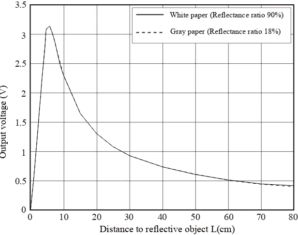
Note 1 : Using reflective object : White paper (Made by Kodak Co., Ltd. gray cards R-27・white face, reflectance; 90%)
Sheet No.: E4-A00201EN
Symbol Rating Unit Supply voltage VCC -0.3 to +7 V
Output terminal voltage VO -0.3 to VCC+0.3 V
Operating temperature Topr -10 to +60 ℃
Storage temperature Tstg -40 to +70 ℃
Parameter
Parameter Symbol Conditions MIN. TYP. MAX. Unit Average supply current ICC L=80cm (Note 1) ― 30 40 mA
Distance measuring ΔL (Note 1) 10 ― 80 cm Output voltage VO L=80cm (Note 1) 0.25 0.4 0.55 V
Output voltage differential ΔVO
Output voltage differece between
L=10cm and L=80cm (Note 1) 1.65 1.9 2.15 V
■
Recommended operating conditions
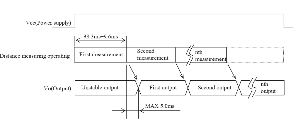
Fig. 1 Timing chart
GP2Y0A21YK0F
Vcc(Power supply)
nth output nth
measurement Second
measurement First measurement
Second output First output
Unstable output
MAX 5.0ms 38.3ms±9.6ms
Distance measuring operating
Vo(Output)
Sheet No.: E4-A00201EN
GP2Y0A21YK0F
Fig. 2 Example of distance measuring characteristics(output)
Distance to reflective object L(cm)
0 10 20 30 40 50 60 70 80
0 0.5 1 1.5 2 2.5 3 3.5
Output voltage (V)
Output voltage (V)
White paper (Reflectance ratio 90%)
Gray paper (Reflectance ratio 18%)
Inverse number of distance (1/cm)
0 0.05 0.1 0.15 0.2
White paper (Reflectance ratio 90%)
Gray paper (Reflectance ratio 18%)
0 0.5 1 1.5 2 2.5 3 3.5
80cm 50cm 40cm
30cm 25cm
20cm 15cm
10cm 8cm
7cm 6cm
5cm
Sheet No.: E4-A00201EN
GP2Y0A21YK0F
Sheet No.: E4-A00201EN
■
Notes
●
Advice for the optics• The lens of this device needs to be kept clean. There are cases that dust, water or oil and so on deteriorate the characteristics of this device. Please consider in actual application.
• Please don’t do washing. Washing may deteriorate the characteristics of optical system and so on.
Please confirm resistance to chemicals under the actual usage since this product has not been designed against washing.
●
Advice for the characteristics• In case that an optical filter is set in front of the emitter and detector portion, the optical filter which has the most efficient transmittance at the emitting wavelength range of LED for this product (λ = 870 ± 70nm), shall be
recommended to use. Both faces of the filter should be mirror polishing. Also, as there are cases that the characteristics may not be satisfied according to the distance between the protection cover and this product or the thickness of the protection cover, please use this product after confirming the operation sufficiently in actual application.
• In case that there is an object near to emitter side of the sensor between sensor and a detecting object, please use this device after confirming sufficiently that the characteristics of this sensor do not change by the object.
• When the detector is exposed to the direct light from the sun, tungsten lamp and so on, there are cases that it can not measure the distance exactly. Please consider the design that the detector is not exposed to the direct light from such light source.
• Distance to a mirror reflector can not be sometimes measured exactly.
In case of changing the mounting angle of this product, it may measure the distance exactly.
• In case that reflective object has boundary line which material or color etc. are excessively different, in order to decrease deviation of measuring distance, it shall be recommended to set the sensor that the direction of boundary line and the line between emitter center and detector center are in parallel.
• In order to decrease deviation of measuring distance by moving direction of the reflective object, it shall be recommended to set the sensor that the moving direction of the object and the line between emitter center and detector center are vertical.
●
Advice for the power supply• In order to stabilize power supply line, we recommend to insert a by-pass capacitor of 10μF or more between Vcc and GND near this product.
(Incorrect) (Correct)
(Incorrect)
(Moving direction)
(Correct)
(Moving direction)
●
Notes on handling• There are some possibilities that the internal components in the sensor may be exposed to the excessive mechanical stress. Please be careful not to cause any excessive pressure on the sensor package and also on the PCB while assembling this product.
GP2Y0A21YK0F
Sheet No.: E4-A00201EN
●
Presence of ODC etc.This product shall not contain the following materials.
And they are not used in the production process for this product.
Regulation substances : CFCs, Halon, Carbon tetrachloride, 1.1.1-Trichloroethane (Methylchloroform)
Specific brominated flame retardants such as the PBB and PBDE are not used in this product at all.
This product shall not contain the following materials banned in the RoHS Directive (2002/95/EC). • Lead, Mercury, Cadmium, Hexavalent chromium, Polybrominated biphenyls (PBB), Polybrominated diphenyl ethers (PBDE).
GP2Y0A21YK0F
Sheet No.: E4-A00201EN
■
Package specification
Packaging method
1.Put products of 100pcs. in tray. packing method is showed in the above fig.(Fig.1) 2.Put them(10-tray) in the packing box. Put pads on their top and bottom.
And put pads on each trays(Total 10 sheets) (Fig.2). 3.Seal the packing box with craft tape.
Print the model No.,quantity,inspection date (1000 pcs./a packing box)(Fig.3).
Package composition
Pad
Packing case
Craft tape
Model No. Quantity Date Tray
Product
(2 sheeets/case: top and bottom)
Tray put products (10-tray/case)
Pad
(10 sheeets/case)
(Fig.1)
(Fig.2)
(Fig.3)
■
Important Notices
· The circuit application examples in this publication are provided to explain representative applications of SHARP devices and are not intended to guarantee any circuit design or license any intellectual property rights. SHARP takes no responsibility for any problems related to any intellectual property right of a third party resulting from the use of SHARP's devices.
· Contact SHARP in order to obtain the latest device specifi-cation sheets before using any SHARP device. SHARP reserves the right to make changes in the s p e c i f i c a t i o n s , c h a r a c t e r i s t i c s , d a t a , m a t e r i a l s , structure, and other contents described herein at any time without notice in order to improve design or reliability. Manufacturing locations are also subject to change without notice.
· Observe the following points when using any devices in this publication. SHARP takes no responsibility for damage caused by improper use of the devices which does not meet the conditions and absolute maximum ratings to be used specified in the relevant specification sheet nor meet the following condi-tions:
(i) The devices in this publication are designed for use in general electronic equipment designs such as:
--- Personal computers
--- Office automation equipment
--- Telecommunication equipment [terminal] --- Test and measurement equipment --- Industrial control
--- Audio visual equipment --- Consumer electronics
(ii) Measures such as fail-safe function and redundant design should be taken to ensure reliability and safety when SHARP devices are used for or in connection
with equipment that requires higher reliability such as: --- Transportation control and safety equipment (i.e., aircraft, trains, automobiles, etc.)
--- Traffic signals
--- Gas leakage sensor breakers --- Alarm equipment
--- Various safety devices, etc.
( i i i ) S H A R P d e v i c e s s h a l l n o t b e u s e d f o r o r i n connection with equipment that requires an extremely high level of reliability and safety such as:
--- Space applications
--- Telecommunication equipment [trunk lines] --- Nuclear power control equipment
--- Medical and other life support equipment (e.g., scuba).
· If the SHARP devices listed in this publication fall within the scope of strategic products described in the Foreign Exchange and Foreign Trade Law of Japan, it is necessary to obtain approval to export such SHARP devices.
· This publication is the proprietary product of SHARP and is copyrighted, with all rights reserved. Under the copyright laws, no part of this publication may be r e p r o -d u c e -d o r t r a n s m i t t e -d i n a n y f o r m o r b y a n y means, electronic or mechanical, for any purpose, in whole or in part, without the express written permission of SHARP. Express written permission is also required before any use of this publication may be made by a third party.
· Contact and consult with a SHARP representative if there are any questions about the contents of this publication.
GP2Y0A21YK0F
Sheet No.: E4-A00201EN
TCS3200, TCS3210
PROGRAMMABLE
COLOR LIGHT-TO-FREQUENCY CONVERTER
TAOS099 − JULY 20091
The LUMENOLOGYr Company
r
r
Copyright E 2009, TAOS Inc.
www.taosinc.com
D
High-Resolution Conversion of Light Intensity to FrequencyD
Programmable Color and Full-Scale Output FrequencyD
Communicates Directly With a MicrocontrollerD
Single-Supply Operation (2.7 V to 5.5 V)D
Power Down FeatureD
Nonlinearity Error Typically 0.2% at 50 kHzD
Stable 200 ppm/°C Temperature CoefficientD
Low-Profile Lead (Pb) Free and RoHS Compliant Surface-Mount Package
Description
The TCS3200 and TCS3210 programmable color light-to-frequency converters that combine confi-gurable silicon photodiodes and a current-to-fre-quency converter on a single monolithic CMOS integrated circuit. The output is a square wave (50% duty cycle) with frequency directly propor-tional to light intensity (irradiance).
The full-scale output frequency can be scaled by one of three preset values via two control input pins. Digital inputs and digital output allow direct interface to a microcontroller or other logic circuitry. Output enable (OE) places the output in the high-impedance state for multiple-unit sharing of a microcontroller input line.
In the TCS3200, the light-to-frequency converter reads an 8 x 8 array of photodiodes. Sixteen photodiodes have blue filters, 16 photodiodes have green filters, 16 photodiodes have red filters, and 16 photodiodes are clear with no filters.
In the TCS3210, the light-to-frequency converter reads a 4 x 6 array of photodiodes. Six photodiodes have blue filters, 6 photodiodes have green filters, 6 photodiodes have red filters, and 6 photodiodes are clear with no filters.
The four types (colors) of photodiodes are interdigitated to minimize the effect of non-uniformity of incident irradiance. All photodiodes of the same color are connected in parallel. Pins S2 and S3 are used to select which group of photodiodes (red, green, blue, clear) are active. Photodiodes are 110 µm x 110 µm in size and are on 134-µm centers.
Functional Block Diagram
Light Photodiode Current-to-FrequencyConverter Array
S2 S3 S0 S1 OE
Output
r
r
Texas Advanced Optoelectronic Solutions Inc.
1001 Klein Road S Suite 300 S Plano, TX 75074 S (972) 673-0759
8 S3
7 S2
6 OUT
5 VDD
PACKAGE D 8-LEAD SOIC (TOP VIEW)
S0 1
S1 2
OE 3
GND 4
8 S3
7 S2
6 OUT
5 VDD
TCS3200
S0 1
S1 2
OE 3
GND 4
TCS3200, TCS3210
PROGRAMMABLE
COLOR LIGHT-TO-FREQUENCY CONVERTER
TAOS099 − JULY 20092
r
r
Copyright E 2009, TAOS Inc. The LUMENOLOGY r Company
www.taosinc.com
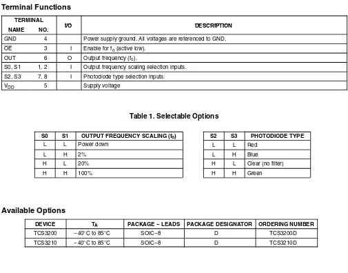
Terminal Functions
TERMINAL
I/O DESCRIPTION
NAME NO. I/O DESCRIPTION
GND 4 Power supply ground. All voltages are referenced to GND.
OE 3 I Enable for fo (active low).
OUT 6 O Output frequency (fo).
S0, S1 1, 2 I Output frequency scaling selection inputs.
S2, S3 7, 8 I Photodiode type selection inputs.
VDD 5 Supply voltage
Table 1. Selectable Options
S0 S1 OUTPUT FREQUENCY SCALING (fo) S2 S3 PHOTODIODE TYPE
L L Power down L L Red
L H 2% L H Blue
H L 20% H L Clear (no filter)
H H 100% H H Green
Available Options
DEVICE TA PACKAGE − LEADS PACKAGE DESIGNATOR ORDERING NUMBER
TCS3200 −40°C to 85°C SOIC−8 D TCS3200D
TCS3200, TCS3210
PROGRAMMABLE
COLOR LIGHT-TO-FREQUENCY CONVERTER
TAOS099 − JULY 20093
The LUMENOLOGYr Company
r
r
Copyright E 2009, TAOS Inc.
www.taosinc.com
Absolute Maximum Ratings over operating free-air temperature range (unless otherwise noted)†
Supply voltage, VDD (see Note 1) . . . 6 V Input voltage range, all inputs, VI . . . −0.3 V to VDD + 0.3 V Operating free-air temperature range, TA (see Note 2) . . . −40°C to 85°C Storage temperature range (see Note 2) . . . −40°C to 85°C Solder conditions in accordance with JEDEC J−STD−020A, maximum temperature (see Note 3) . . . 260°C
†Stresses beyond those listed under “absolute maximum ratings” may cause permanent damage to the device. These are stress ratings only, and
functional operation of the device at these or any other conditions beyond those indicated under “recommended operating conditions” is not implied. Exposure to absolute-maximum-rated conditions for extended periods may affect device reliability.
NOTES: 1. All voltage values are with respect to GND.
2. Long-term storage or operation above 70°C could cause package yellowing that will lower the sensitivity to wavelengths < 500nm.
3. The device may be hand soldered provided that heat is applied only to the solder pad and no contact is made between the tip of the solder iron and the device lead. The maximum time heat should be applied to the device is 5 seconds.
Recommended Operating Conditions
MIN NOM MAX UNIT
Supply voltage, VDD 2.7 5 5.5 V
High-level input voltage, VIH VDD = 2.7 V to 5.5 V 2 VDD V
Low-level input voltage, VIL VDD = 2.7 V to 5.5 V 0 0.8 V
Operating free-air temperature range, TA −40 70 °C
Electrical Characteristics at TA = 25°C, VDD = 5 V (unless otherwise noted)
PARAMETER TEST CONDITIONS MIN TYP MAX UNIT
VOH High-level output voltage IOH = − 2 mA 4 4.5 V
VOL Low-level output voltage IOL = 2 mA 0.25 0.40 V
IIH High-level input current 5 µA
IIL Low-level input current 5 µA
I Supply current
Power-on mode 1.4 2 mA
IDD Supply current Power-down mode 0.1
µA
S0 = H, S1 = H 500 600 kHz
Full-scale frequency (See Note 4) S0 = H, S1 = L 100 120 kHz
Full scale frequency (See Note 4)
S0 = L, S1 = H 10 12 kHz
Temperature coefficient of responsivity λ≤ 700 nm, −25°C ≤ TA≤ 70°C ±200 ppm/°C
kSVS Supply voltage sensitivity VDD = 5 V ±10% ±0.5 %/ V
TCS3200, TCS3210
PROGRAMMABLE
COLOR LIGHT-TO-FREQUENCY CONVERTER
TAOS099 − JULY 20094
r
r
Copyright E 2009, TAOS Inc. The LUMENOLOGY r Company
www.taosinc.com
Operating Characteristics at VDD = 5 V, TA = 25
°
C, S0 = H, S1 = H (unless otherwise noted) (See Notes 5, 6, 7, and 8). Values for TCS3200 (TCS3210) are below.PARAMETER TEST CONDITIONS
CLEAR PHOTODIODE S2 = H, S3 = L
BLUE PHOTODIODE S2 = L, S3 = H
GREEN PHOTODIODE S2 = H, S3 = H
RED PHOTODIODE
S2 = L, S3 = L UNIT CONDITIONS
MIN TYP MAX MIN TYP MAX MIN TYP MAX MIN TYP MAX
Ee = 47.2 µW/cm2, 12.5 15.6 18.7 61% 84% 22% 43% 0% 6%
Ee = 47.2 µW/cm2,
λp = 470 nm (4.7) (5.85) (7) 61% 84% 22% 43% 0% 6%
f
Output
frequency Ee = 40.4 µW/cm2, 12.5 15.6 18.7 8% 28% 57% 80% 9% 27% kHz
fO frequency
(Note 9)
Ee = 40.4 µW/cm2,
λp = 524 nm (4.7) (5.85) (7)
8% 28% 57% 80% 9% 27% kHz
(Note 9)
Ee = 34.6 µW/cm2, 13.1 16.4 19.7
5% 21% 0% 12% 84% 105%
Ee = 34.6 µW/cm2,
λp = 640 nm (4.9) (6.15) (7.4) 5% 21% 0% 12% 84% 105%
λ 470 nm
331
61% 84% 22% 43% 0% 6%
λp = 470 nm (124) 61% 84% 22% 43% 0% 6%
R
Irradiance
responsivity λ 524 nm 386 8% 28% 57% 80% 9% 27%
Hz/ ( W/
Re responsivity
(Note 10)
λp = 524 nm
(145) 8% 28% 57% 80% 9% 27% (cmµW/2)
(Note 10)
λ 640 nm 474 5% 21% 0% 12% 84% 105%
cm2)
λp = 640 nm (178) 5% 21% 0% 12% 84% 105%
λ 470 nm
1813
λp = 470 nm (4839) −− −− −−
Saturation
irradiance λ 524 nm 1554 µW/
irradiance (Note 11)
λp = 524 nm
(4138) −− −− −−
µW/
cm2
(Note 11)
λ 640 nm 1266
λp = 640 nm (3371) −− −− −−
fD
Dark
frequency Ee = 0 2 10 2 10 2 10 2 10 Hz
fO = 0 to 5 kHz ±0.1 ±0.1 ±0.1 ±0.1
Nonlinearity
(Note 12) fO = 0 to 50 kHz ±0.2 ±0.2 ±0.2 ±0.2 % F.S.
(Note 12)
fO = 0 to 500 kHz ±0.5 ±0.5 ±0.5 ±0.5
% F.S.
Recovery from power down
100 100 100 100 µs
Response time to out-put enable (OE)
100 100 100 100 ns
NOTES: 5. Optical measurements are made using small-angle incident radiation from a light-emitting diode (LED) optical source.
6. The 470 nm input irradiance is supplied by an InGaN light-emitting diode with the following characteristics:
peak wavelength λp = 470 nm, spectral halfwidth Δλ½ = 35 nm, and luminous efficacy = 75 lm/W.
7. The 524 nm input irradiance is supplied by an InGaN light-emitting diode with the following characteristics:
peak wavelength λp = 524 nm, spectral halfwidth Δλ½ = 47 nm, and luminous efficacy = 520 lm/W.
8. The 640 nm input irradiance is supplied by a AlInGaP light-emitting diode with the following characteristics:
peak wavelength λp = 640 nm, spectral halfwidth Δλ½ = 17 nm, and luminous efficacy = 155 lm/W.
9. Output frequency Blue, Green, Red percentage represents the ratio of the respective color to the Clear channel absolute value.
10. Irradiance responsivity Re is characterized over the range from zero to 5 kHz.
11. Saturation irradiance = (full-scale frequency)/(irradiance responsivity) for the Clear reference channel.
TCS3200, TCS3210
PROGRAMMABLE
COLOR LIGHT-TO-FREQUENCY CONVERTER
TAOS099 − JULY 20095
The LUMENOLOGYr Company
r
r
Copyright E 2009, TAOS Inc.
www.taosinc.com
TYPICAL CHARACTERISTICS
Figure 1
300 500 700 900
Relative Responsivity
1100
λ − Wavelength − nm
PHOTODIODE SPECTRAL RESPONSIVITY
0.1 0.2 0.3 0.4 0.5 0.6 0.7 0.8 0.9 1 0 Blue
TA = 25°C
Green
Normalized to Clear @ 715 nm
Red Blue
Green Clear
Figure 2
NORMALIZED OUTPUT FREQUENCY vs.
ANGULAR DISPLACEMENT
Q − Angular Displacement − °
fO
— Output Frequency — Normalized
0 0.2 0.4 0.6 0.8 1
−90 −60 −30 0 30 60 90
Optical Axis
Angular Displacement is Equal for Both Aspects
Figure 3
IDD vs.
VDD vs.
TEMPERATURE 1.05 1.1 1.15 1.2 1.25 1.3 1.35 1.4 1.45 1.5 1 1.55
0 25 50 75 100
TA − Free-Air Temperature −°C
IDD
— mA
Saturated VDD = 5 V
Saturated VDD = 3 V
Dark VDD = 3 V
Dark VDD = 5 V
Figure 4
NORMALIZED OUTPUT vs.
VDD
VDD − V
Normalized Output — %
TCS3200, TCS3210
PROGRAMMABLE
COLOR LIGHT-TO-FREQUENCY CONVERTER
TAOS099 − JULY 20096
r
r
Copyright E 2009, TAOS Inc. The LUMENOLOGY r Company
www.taosinc.com
TYPICAL CHARACTERISTICS
Figure 5
λ − Wavelength of Incident Light − nm
PHOTODIODE RESPONSIVITY TEMPERATURE COEFFICIENT vs.
WAVELENGTH OF INCIDENT LIGHT
T
emperature
Coefficient — ppm/deg C
600 650 700 750 800 850 900 950 1000 1k
2k 3k 4k 5k 6k 7k 8k 9k
TCS3200, TCS3210
PROGRAMMABLE
COLOR LIGHT-TO-FREQUENCY CONVERTER
TAOS099 − JULY 20097
The LUMENOLOGYr Company
r
r
Copyright E 2009, TAOS Inc.
www.taosinc.com
APPLICATION INFORMATION
Power supply considerations
Power-supply lines must be decoupled by a 0.01-µF to 0.1-µF capacitor with short leads mounted close to the device package.
Input interface
A low-impedance electrical connection between the device OE pin and the device GND pin is required for improved noise immunity. All input pins must be either driven by a logic signal or connected to VDD or GND — they should not be left unconnected (floating).
Output interface
The output of the device is designed to drive a standard TTL or CMOS logic input over short distances. If lines greater than 12 inches are used on the output, a buffer or line driver is recommended.
A high state on Output Enable (OE) places the output in a high-impedance state for multiple-unit sharing of a microcontroller input line.
Power down
Powering down the sensor using S0/S1 (L/L) will cause the output to be held in a high-impedance state. This is similar to the behavior of the output enable pin, however powering down the sensor saves significantly more power than disabling the sensor with the output enable pin.
Photodiode type (color) selection
The type of photodiode (blue, green, red, or clear) used by the device is controlled by two logic inputs, S2 and S3 (see Table 1).
Output frequency scaling
Output-frequency scaling is controlled by two logic inputs, S0 and S1. The internal light-to-frequency converter generates a fixed-pulsewidth pulse train. Scaling is accomplished by internally connecting the pulse-train output of the converter to a series of frequency dividers. Divided outputs are 50%-duty cycle square waves with relative frequency values of 100%, 20%, and 2%. Because division of the output frequency is accomplished by counting pulses of the principal internal frequency, the final-output period represents an average of the multiple periods of the principle frequency.
The output-scaling counter registers are cleared upon the next pulse of the principal frequency after any transition of the S0, S1, S2, S3, and OE lines. The output goes high upon the next subsequent pulse of the principal frequency, beginning a new valid period. This minimizes the time delay between a change on the input lines and the resulting new output period. The response time to an input programming change or to an irradiance step change is one period of new frequency plus 1 µs. The scaled output changes both the full-scale frequency and the dark frequency by the selected scale factor.
TCS3200, TCS3210
PROGRAMMABLE
COLOR LIGHT-TO-FREQUENCY CONVERTER
TAOS099 − JULY 20098
r
r
Copyright E 2009, TAOS Inc. The LUMENOLOGY r Company
www.taosinc.com
APPLICATION INFORMATION
Measuring the frequency
The choice of interface and measurement technique depends on the desired resolution and data acquisition rate. For maximum data-acquisition rate, period-measurement techniques are used.
Output data can be collected at a rate of twice the output frequency or one data point every microsecond for full-scale output. Period measurement requires the use of a fast reference clock with available resolution directly related to reference clock rate. Output scaling can be used to increase the resolution for a given clock rate or to maximize resolution as the light input changes. Period measurement is used to measure rapidly varying light levels or to make a very fast measurement of a constant light source.
Maximum resolution and accuracy may be obtained using frequency-measurement, pulse-accumulation, or integration techniques. Frequency measurements provide the added benefit of averaging out random- or high-frequency variations (jitter) resulting from noise in the light signal. Resolution is limited mainly by available counter registers and allowable measurement time. Frequency measurement is well suited for slowly varying or constant light levels and for reading average light levels over short periods of time. Integration (the accumulation of pulses over a very long period of time) can be used to measure exposure, the amount of light present in an area over a given time period.
PCB Pad Layout
Suggested PCB pad layout guidelines for the D package are shown in Figure 6.
2.25 6.90 4.65
1.27
0.50
NOTES: A. All linear dimensions are in millimeters.
B. This drawing is subject to change without notice.
TCS3200, TCS3210
PROGRAMMABLE
COLOR LIGHT-TO-FREQUENCY CONVERTER
TAOS099 − JULY 20099
The LUMENOLOGYr Company
r
r
Copyright E 2009, TAOS Inc.
www.taosinc.com
MECHANICAL INFORMATION
This SOIC package consists of an integrated circuit mounted on a lead frame and encapsulated with an electrically nonconductive clear plastic compound. The TCS3200 has an 8
×
8 array of photodiodes with a total size of 1 mm by 1 mm. The photodiodes are 110 µm×
110 µm in size and are positioned on 134 µm centers.PACKAGE D PLASTIC SMALL-OUTLINE
A
1.75 1.35
0.50 0.25
4.00 3.80
6.20 5.80 455
0.88 TYP TOP OF SENSOR DIE
5.00 4.80
5.3 MAX
1.27
0.41 0.250.10 0.25 0.19
DETAIL A
PIN 1
6 y 1.27 8y0.5100.330
j2.8 TYP CLEAR WINDOW 2.12
+ 0.250 3.00 + 0.250 NOTE B
Pb
PIN 1
TOP VIEW BOTTOM VIEW
SIDE VIEW
END VIEW
NOTES: A. All linear dimensions are in millimeters.
B. The center of the 1-mm by 1-mm photo-active area is referenced to the upper left corner tip of the lead frame (Pin 1). C. Package is molded with an electrically nonconductive clear plastic compound having an index of refraction of 1.55. D. This drawing is subject to change without notice.
TCS3200, TCS3210
PROGRAMMABLE
COLOR LIGHT-TO-FREQUENCY CONVERTER
TAOS099 − JULY 200910
r
r
Copyright E 2009, TAOS Inc. The LUMENOLOGY r Company
www.taosinc.com
MECHANICAL INFORMATION
This SOIC package consists of an integrated circuit mounted on a lead frame and encapsulated with an electrically nonconductive clear plastic compound. The TCS3210 has a 4
×
6 array of photodiodes with a total size of 0.54 mm by 0.8 mm. The photodiodes are 110 µm×
110 µm in size and are positioned on 134 µm centers.PACKAGE D PLASTIC SMALL-OUTLINE
A
1.75 1.35
0.50 0.25
4.00 3.80
6.20 5.80 455
0.88 TYP TOP OF SENSOR DIE
5.00 4.80
5.3 MAX
1.27
0.41 0.250.10 0.25 0.19
DETAIL A
PIN 1
6 y 1.27 8y 0.5100.330
j2.8 TYP CLEAR WINDOW 2.12
+ 0.250 3.00 + 0.250 NOTE B
Pb
PIN 1
TOP VIEW BOTTOM VIEW
SIDE VIEW
END VIEW
NOTES: A. All linear dimensions are in millimeters.
B. The center of the 0.54-mm by 0.8-mm photo-active area is referenced to the upper left corner tip of the lead frame (Pin 1). C. Package is molded with an electrically nonconductive clear plastic compound having an index of refraction of 1.55. D. This drawing is subject to change without notice.
TCS3200, TCS3210
PROGRAMMABLE
COLOR LIGHT-TO-FREQUENCY CONVERTER
TAOS099 − JULY 200911
The LUMENOLOGYr Company
r
r
Copyright E 2009, TAOS Inc.
www.taosinc.com
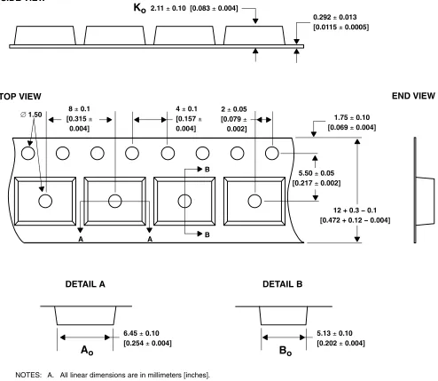
MECHANICAL INFORMATION
0.292 + 0.013 [0.0115 + 0.0005] 2.11 + 0.10 [0.083 + 0.004]
2 + 0.05 [0.079 +
0.002] 4 + 0.1
[0.157 +
0.004]
1.75 + 0.10 [0.069 + 0.004]
12 + 0.3 − 0.1 [0.472 + 0.12 − 0.004]
SIDE VIEW
TOP VIEW END VIEW
DETAIL B
5.50 + 0.05 [0.217 + 0.002] 8 + 0.1
[0.315 +
0.004]
j 1.50
B
B
A A
6.45 + 0.10 [0.254 + 0.004]
5.13 + 0.10 [0.202 + 0.004]
DETAIL A
A
oB
oK
oNOTES: A. All linear dimensions are in millimeters [inches].
B. The dimensions on this drawing are for illustrative purposes only. Dimensions of an actual carrier may vary slightly.
C. Symbols on drawing Ao, Bo, and Ko are defined in ANSI EIA Standard 481−B 2001.
D. Each reel is 178 millimeters in diameter and contains 1000 parts.
E. TAOS packaging tape and reel conform to the requirements of EIA Standard 481−B. F. This drawing is subject to change without notice.
TCS3200, TCS3210
PROGRAMMABLE
COLOR LIGHT-TO-FREQUENCY CONVERTER
TAOS099 − JULY 200912
r
r
Copyright E 2009, TAOS Inc. The LUMENOLOGY r Company
www.taosinc.com
MANUFACTURING INFORMATION
The Plastic Small Outline IC package (D) has been tested and has demonstrated an ability to be reflow soldered to a PCB substrate.
The solder reflow profile describes the expected maximum heat exposure of components during the solder reflow process of product on a PCB. Temperature is measured on top of component. The component should be limited to a maximum of three passes through this solder reflow profile.
Table 2. TCS3200, TCS3210 Solder Reflow Profile
PARAMETER REFERENCE TCS32x0
Average temperature gradient in preheating 2.5°C/sec
Soak time tsoak 2 to 3 minutes
Time above 217°C t1 Max 60 sec
Time above 230°C t2 Max 50 sec
Time above Tpeak −10°C t3 Max 10 sec
Peak temperature in reflow Tpeak 260° C (−0°C/+5°C)
Temperature gradient in cooling Max −5°C/sec
t3
t2
t1
tsoak
T3
T2
T1
Tpeak
Not to scale — for reference only
Time (sec)
T
emperature (
5
C)
TCS3200, TCS3210
PROGRAMMABLE
COLOR LIGHT-TO-FREQUENCY CONVERTER
TAOS099 − JULY 200913
The LUMENOLOGYr Company
r
r
Copyright E 2009, TAOS Inc.
www.taosinc.com
Moisture Sensitivity
Optical characteristics of the device can be adversely affected during the soldering process by the release and vaporization of moisture that has been previously absorbed into the package molding compound. To prevent these adverse conditions, all devices shipped in carrier tape have been pre-baked and shipped in a sealed moisture-barrier bag. No further action is necessary if these devices are processed through solder reflow within 24 hours of the seal being broken on the moisture-barrier bag.
However, for all devices shipped in tubes or if the seal on the moisture barrier bag has been broken for 24 hours or longer, it is recommended that the following procedures be used to ensure the package molding compound contains the smallest amount of absorbed moisture possible.
For devices shipped in tubes:
1. Remove devices from tubes
2. Bake devices for 4 hours, at 90°C
3. After cooling, load devices back into tubes
4. Perform solder reflow within 24 hours after bake
Bake only a quantity of devices that can be processed through solder reflow in 24 hours. Devices can be re-baked for 4 hours, at 90°C for a cumulative total of 12 hours (3 bakes for 4 hours at 90°C).
For devices shipped in carrier tape:
1. Bake devices for 4 hours, at 90°C in the tape
2. Perform solder reflow within 24 hours after bake
TCS3200, TCS3210
PROGRAMMABLE
COLOR LIGHT-TO-FREQUENCY CONVERTER
TAOS099 − JULY 200914
r
r
Copyright E 2009, TAOS Inc. The LUMENOLOGY r Company
www.taosinc.com
PRODUCTION DATA — information in this document is current at publication date. Products conform to specifications in accordance with the terms of Texas Advanced Optoelectronic Solutions, Inc. standard warranty. Production processing does not necessarily include testing of all parameters.
LEAD-FREE (Pb-FREE) and GREEN STATEMENT
Pb-Free (RoHS) TAOS’ terms Lead-Free or Pb-Free mean semiconductor products that are compatible with the current
RoHS requirements for all 6 substances, including the requirement that lead not exceed 0.1% by weight in homogeneous materials. Where designed to be soldered at high temperatures, TAOS Pb-Free products are suitable for use in specified lead-free processes.
Green (RoHS & no Sb/Br) TAOS defines Green to mean Pb-Free (RoHS compatible), and free of Bromine (Br) and
Antimony (Sb) based flame retardants (Br or Sb do not exceed 0.1% by weight in homogeneous material).
Important Information and Disclaimer The information provided in this statement represents TAOS’ knowledge and belief as of the date that it is provided. TAOS bases its knowledge and belief on information provided by third parties, and makes no representation or warranty as to the accuracy of such information. Efforts are underway to better integrate information from third parties. TAOS has taken and continues to take reasonable steps to provide representative and accurate information but may not have conducted destructive testing or chemical analysis on incoming materials and chemicals. TAOS and TAOS suppliers consider certain information to be proprietary, and thus CAS numbers and other limited information may not be available for release.
NOTICE
Texas Advanced Optoelectronic Solutions, Inc. (TAOS) reserves the right to make changes to the products contained in this document to improve performance or for any other purpose, or to discontinue them without notice. Customers are advised to contact TAOS to obtain the latest product information before placing orders or designing TAOS products into systems.
TAOS assumes no responsibility for the use of any products or circuits described in this document or customer product design, conveys no license, either expressed or implied, under any patent or other right, and makes no representation that the circuits are free of patent infringement. TAOS further makes no claim as to the suitability of its products for any particular purpose, nor does TAOS assume any liability arising out of the use of any product or circuit, and specifically disclaims any and all liability, including without limitation consequential or incidental damages.