POWER
ELECTRONICS
T H E
Titles included in the series
Supervised and Unsupervised Pattern Recognition: Feature Extraction and Computational Intelligence
Evangelia Micheli-Tzanakou, Rutgers University
Switched Reluctance Motor Drives: Modeling, Simulation, Analysis, Design, and Applications
R. Krishnan, Virginia Tech
The Power Electronics Handbook
Timothy L. Skvarenina, Purdue University
The Handbook of Applied Computational Intelligence
Mary Lou Padgett, Auburn University
Nicolaos B. Karayiannis, University of Houston
Lofti A. Zadeh, University of California, Berkeley
The Handbook of Applied Neurocontrols
Mary Lou Padgett, Auburn University
Charles C. Jorgensen, NASA Ames Research Center
Paul Werbos, National Science Foundation
I n d u s t r i a l E l e c t r o n i c s S e r i e s
Series Editor
C RC P R E S S
Boca Raton London New York Washington, D.C.
POWER
ELECTRONICS
T H E
Edited by
TIMOTHY L. SKVARENINA
Purdue University
West Lafayette, Indiana
Industrial Electronics Series
This book contains information obtained from authentic and highly regarded sources. Reprinted material is quoted with permission, and sources are indicated. A wide variety of references are listed. Reasonable efforts have been made to publish reliable data and information, but the authors and the publisher cannot assume responsibility for the validity of all materials or for the consequences of their use.
Neither this book nor any part may be reproduced or transmitted in any form or by any means, electronic or mechanical, including photocopying, microfilming, and recording, or by any information storage or retrieval system, without prior permission in writing from the publisher.
All rights reserved. Authorization to photocopy items for internal or personal use, or the personal or internal use of specific clients, may be granted by CRC Press LLC, provided that $1.50 per page photocopied is paid directly to Copyright Clearance Center, 222 Rosewood Drive, Danvers, MA 01923 USA The fee code for users of the Transactional Reporting Service is ISBN 0-8493-7336-0/02/$0.00+$1.50. The fee is subject to change without notice. For organizations that have been granted a photocopy license by the CCC, a separate system of payment has been arranged.
The consent of CRC Press LLC does not extend to copying for general distribution, for promotion, for creating new works, or for resale. Specific permission must be obtained in writing from CRC Press LLC for such copying.
Direct all inquiries to CRC Press LLC, 2000 N.W. Corporate Blvd., Boca Raton, Florida 33431.
Trademark Notice: Product or corporate names may be trademarks or registered trademarks, and are used only for identification and explanation, without intent to infringe.
Visit the CRC Press Web site at www.crcpress.com
© 2002 by CRC Press LLC
No claim to original U.S. Government works International Standard Book Number 0-8493-7336-0
Library of Congress Card Number 2001043047 Printed in the United States of America 1 2 3 4 5 6 7 8 9 0
Printed on acid-free paper
Library of Congress Cataloging-in-Publication Data
The power electronics handbook / edited by Timothy L. Skvarenina. p. cm. — (Industrial electronics series)
Includes bibliographical references and index. ISBN 0-8493-7336-0 (alk. paper)
1. Power electronics. I. Skvarenina, Timothy L. II. Series.
TK7881.15 .P673 2001
Preface
Introduction
The control of electric power with power electronic devices has become increasingly important over the last 20 years. Whole new classes of motors have been enabled by power electronics, and the future offers the possibility of more effective control of the electric power grid using power elec-tronics. The Power Electronics Handbook is intended to provide a reference that is both concise and useful for individuals, ranging from students in engineering to experienced, practicing professionals. The Handbook covers the very wide range of topics that comprise the subject of power electronics blending many of the traditional topics with the new and innovative technologies that are at the leading edge of advances being made in this subject. Emphasis has been placed on the practical application of the technologies discussed to enhance the value of the book to the reader and to enable a clearer understanding of the material. The presentations are deliberately tutorial in nature, and examples of the practical use of the technology described have been included.
The contributors to this Handbook span the globe and include some of the leading authorities in their areas of expertise. They are from industry, government, and academia. All of them have been chosen because of their intimate knowledge of their subjects as well as their ability to present them in an easily understandable manner.
Organization
The book is organized into three parts. Part I presents an overview of the semiconductor devices that are used, or projected to be used, in power electronic devices. Part II explains the operation of circuits used in power electronic devices, and Part III describes a number of applications for power electronics, including motor drives, utility applications, and electric vehicles.
Acknowledgments
The Editor
Timothy L. Skvarenina received his B.S.E.E. and M.S.E.E. degrees from the Illinois Institute of
Tech-nology in 1969 and 1970, respectively, and his Ph.D. in electrical engineering from Purdue University in 1979. In 1970, he entered active duty with the U.S. Air Force, where he served 21 years, retiring as a lieutenant colonel in 1991. During his Air Force career, he spent 6 years designing, constructing, and inspecting electric power distribution projects for a variety of facilities. He also was assigned to the faculty of the Air Force Institute of Technology (AFIT) for 3 years, where he taught and researched conventional power systems and pulsed-power systems, including railguns, high-power switches, and magnetocumulative generators. Dr. Skvarenina received the Air Force Meritorious Service Medal for his contributions to the AFIT curriculum in 1984. He also spent 4 years with the Strategic Defense Initiative Office (SDIO), where he conducted and directed large-scale systems analysis studies. He received the Department of Defense Superior Service Medal in 1991 for his contributions to SDIO.
In 1991, Dr. Skvarenina joined the faculty of the School of Technology at Purdue University, where he currently teaches undergraduate courses in electrical machines and power systems, as well as a graduate course in facilities engineering. He is a senior member of the IEEE; a member of the American Society for Engineering Education (ASEE), Tau Beta Pi, and Eta Kappa Nu; and a registered professional engineer in the state of Colorado.
Dr. Skvarenina has been active in both IEEE and ASEE. He has held the offices of secretary, vice-chair, and chair of the Central Indiana chapter of the IEEE Power Engineering Society. At the national level he is a member of the Power Engineering Society Education Committee. He has also been active in the IEEE Education Society, serving as an associate editor of the Transactions on Education
and co-program chair for the 1999 and 2003 Frontiers in Education Conferences. For his activity and contributions to the Education Society, he received the IEEE Third Millennium Medal in 2000. Within ASEE, Dr. Skvarenina has been an active member of the Energy Conversion and Conser-vation Division, serving in a series of offices including division chair. In 1999, he was elected by the ASEE membership to the Board of Directors for a 2-year term as Chair, Professional Interest Council III. In June 2000, he was elected by the Board of Directors as Vice-President for Profession Interest Councils for the year 2000–2001.
Editorial Advisors
Mariesa Crow
University of Missouri-Rolla Rolla, Missouri
Farhad Nozari
Boeing Corporation Seattle, Washington
Scott Sudhoff
Purdue University West Lafayette, Indiana
Annette von Jouanne
Oregon State University Corvallis, Oregon
Oleg Wasynczuk
Contributors
Ali Agah
Sharif University of Technology Tehran, Iran
Ashish Agrawal
University of Alaska Fairbanks Fairbanks, Alaska
Hirofumi Akagi
Tokyo Institute of Technology Tokyo, Japan
Sohail Anwar
Pennsylvania State University Altoona, Pennsylvania
Rajapandian Ayyanar
Arizona State University Tempe, Arizona
Vrej Barkhordarian
International Rectifier El Segundo, California
Ronald H. Brown
Marquette University Milwaukee, Wisconsin
Patrick L. Chapman
University of Illinois at Urbana-Champaign Urbana, Illinois
Badrul H. Chowdhury
University of Missouri-Rolla Rolla, Missouri
Keith Corzine
University of Wisconsin- Milwaukee
Milwaukee, Wisconsin
Dariusz Czarkowski
Polytechnic University Brooklyn, New York
Alexander Domijan, Jr.
University of Florida Gainesville, Florida
Mehrdad Ehsani
Texas A&M University College Station, Texas
Ali Emadi
Illinois Institute of Technology Chicago, Illinois
Ali Feliachi
West Virginia University Morgantown, West Virginia
Wayne Galli
Southwest Power Pool Little Rock, Arkansas
Michael Giesselmann
Texas Tech University Lubbock, Texas
Tilak Gopalarathnam
Texas A&M University College Station, Texas
Sam Guccione
Eastern Illinois University Charleston, Illinois
Sándor Halász
Budapest University of Technology and Economics Budapest, Hungary
Azra Hasanovic
West Virginia University Morgantown, West Virginia
John Hecklesmiller
Best Power Technology, Inc. Nededah, Wisconsin
Alex Q. Huang
Virginia Polytechnic Institute and State University Blacksburg, Virginia
Iqbal Husain
The University of Akron Akron, Ohio
Amit Kumar Jain
University of Minnesota Minneapolis, Minnesota
Attila Karpati
Philip T. Krein
University of Illinois at Urbana-Champaign Urbana, Illinois
Dave Layden
Best Power Technology, Inc. Nededah, Wisconsin
Daniel Logue
University of Illinois at Urbana-Champaign Urbana, Illinois
Javad Mahdavi
Sharif University of Technology Tehran, IranPaolo Mattavelli
University of Padova Padova, Italy
Roger Messenger
Florida Atlantic University Boca Raton, Florida
István Nagy
Budapest University of Technology and Economics Budapest, Hungary
Tahmid Ur Rahman
Texas A&M University College Station, Texas
Kaushik Rajashekara
Delphi Automotive Systems Kokomo, Indiana
Michael E. Ropp
South Dakota State University Brookings, South Dakota
Hossein Salehfar
University of North Dakota Grand Forks, North Dakota
Bipin Satavalekar
University of Alaska Fairbanks Fairbanks, Alaska
Karl Schoder
West Virginia University Morgantown, West Virginia
Daniel Jeffrey Shortt
Cedarville University Cedarville, Ohio
Timothy L. Skvarenina
Purdue University West Lafayette, Indiana
Zhidong Song
University of Florida Gainesville, Florida
Giorgio Spiazzi
University of Padova Padova, Italy
Ana Stankovic
Cleveland State University Cleveland, Ohio
Ralph Staus
Pennsylvania State University Reading, Pennsylvania
Laura Steffek
Best Power Technology, Inc. Nededah, Wisconsin
Roman Stemprok
University of North Texas Denton, Texas
Mahesh M. Swamy
Yaskawa Electric America Waukegan, Illinois
Hamid A. Toliyat
Texas A&M University College Station, Texas
Eric Walters
P. C. Krause and Associates West Lafayette, Indiana
Oleg Wasynczuk
Purdue University West Lafayette, Indiana
Richard W. Wies
University of Alaska Fairbanks Fairbanks, Alaska
Brian Young
Contents
PART I
Power Electronic Devices
1
Power Electronics
1.1 Overview Kaushik Rajashekara
1.2 Diodes Sohail Anwar
1.3 Schottky Diodes Sohail Anwar
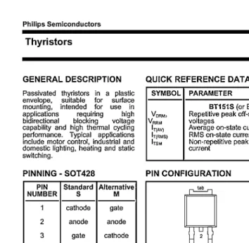
1.4 Thyristors Sohail Anwar
1.5 Power Bipolar Junction Transistors Sohail Anwar
1.6 MOSFETs Vrej Barkhordarian
1.7 General Power Semiconductor Switch Requirements Alex Q. Huang
1.8 Gate Turn-Off Thyristors Alex Q. Huang
1.9 Insulated Gate Bipolar Transistors Alex Q. Huang
1.10 Gate-Commutated Thyristors and Other Hard-Driven GTOs Alex Q. Huang
1.11 Comparison Testing of Switches Alex Q. Huang
PART II
Power Electronic Circuits and Controls
2
DC-DC Converters
2.1 Overview Richard Wies, Bipin Satavalekar, and Ashish Agrawal
2.2 Choppers Javad Mahdavi, Ali Agah, and Ali Emadi
2.3 Buck Converters Richard Wies, Bipin Satavalekar, and Ashish Agrawal
2.4 Boost Converters Richard Wies, Bipin Satavalekar, and Ashish Agrawal
2.5 Cúk Converter Richard Wies, Bipin Satavalekar, and Ashish Agrawal
2.6 Buck–Boost Converters Daniel Jeffrey Shortt
3
AC-AC Conversion
Sándor Halász
3.1 Introduction
3.2 Cycloconverters
3.3 Matrix Converters
4
Rectifiers
4.1 Uncontrolled Single-Phase Rectifiers Sam Guccione
4.2 Uncontrolled and Controlled Rectifiers Mahesh M. Swamy
5
Inverters
5.1 Overview Michael Giesselmann
5.2 DC-AC Conversion Attila Karpati
5.3 Resonant Converters István Nagy
5.4 Series-Resonant Inverters Dariusz Czarkowski
5.5 Resonant DC-Link Inverters Michael B. Ropp
5.6 Auxiliary Resonant Commutated Pole Inverters Eric Walters and Oleg Wasynczuk
6 Multilevel Converters Keith Corzine
6.1 Introduction
6.2 Multilevel Voltage Source Modulation
6.3 Fundamental Multilevel Converter Topologies
6.4 Cascaded Multilevel Converter Topologies
6.5 Multilevel Converter Laboratory Examples
6.6 Conclusion
7 Modulation Strategies
7.1 Introduction Michael Giesselmann
7.2 Six-Step Modulation Michael Giesselmann
7.3 Pulse Width Modulation Michael Giesselmann
7.4 Third Harmonic Injection for Voltage Boost of SPWM Signals Michael Giesselmann
7.5 Generation of PWM Signals Using Microcontrollers and DSPs Michael Giesselmann
7.6 Voltage-Source-Based Current Regulation Michael Giesselmann
7.7 Hysteresis Feedback Control Hossein Salehfar
7.8 Space-Vector Pulse Width Modulation Hamid A. Toliyat and Tahmid Ur Rahman
8 Sliding-Mode Control of Switched-Mode Power Supplies
Giorgio Spiazzi and Paolo Mattavelli
8.1 Introduction
8.2 Introduction to Sliding-Mode Control
8.3 Basics of Sliding-Mode Theory
8.4 Application of Sliding-Mode Control to DC-DC Converters—Basic Principle
8.5 Sliding-Mode Control of Buck DC-DC Converters
8.6 Extension to Boost and Buck–Boost DC-DC Converters
8.7 Extension to Cúk and SEPIC DC-DC Converters
8.8 General-Purpose Sliding-Mode Control Implementation
Part III
Applications and Systems Considerations
9 DC Motor Drives Ralph Staus
9.1 DC Motor Basics
9.2 DC Speed Control
9.3 DC Drive Basics
9.4 Transistor PWM DC Drives
9.5 SCR DC Drives
10 AC Machines Controlled as DC Machines
(Brushless DC Machines/Electronics) Hamid A. Toliyat
and Tilak Gopalarathnam
10.1 Introduction
10.2 Machine Construction
10.3 Motor Characteristics
10.4 Power Electronic Converter
10.5 Position Sensing
10.6 Pulsating Torque Components
10.7 Torque-Speed Characteristics
10.8 Applications
11
Control of Induction Machine Drives
Daniel Logue and Philip T. Krein
11.1 Introduction
11.2 Scalar Induction Machine Control
11.3 Vector Control of Induction Machines
11.4 Summary
12
Permanent-Magnet Synchronous Machine Drives
Patrick L. Chapman
12.1 Introduction
12.2 Construction of PMSM Drive Systems
12.3 Simulation and Model
12.4 Controlling the PMSM
12.5 Advanced Topics in PMSM Drives
13 Switched Reluctance Machines Iqbal Husain
13.1 Introduction
13.2 SRM Configuration
13.3 Basic Principle of Operation
13.4 Design
13.5 Converter Topologies
13.6 Control Strategies
14 Step Motor Drives Ronald H. Brown
14.1 Introduction
14.2 Types and Operation of Step Motors
14.3 Step Motor Models
14.4 Control of Step Motors
15
Servo Drives
Sándor Halász
15.1 DC Drives
15.2 Induction Motor Drives
16
Uninterruptible Power Supplies
Laura Steffek, John Hacklesmiller,
Dave Layden, and Brian Young
16.1 UPS Functions
16.2 Static UPS Topologies
16.3 Rotary UPSs
16.4 Alternate AC and DC Sources
17
Power Quality and Utility Interface Issues
17.1 Overview Wayne Galli
17.2 Power Quality Considerations Timothy L. Skvarenina
17.3 Passive Harmonic Filters Badrul H. Chowdhury
17.4 Active Filters for Power Conditioning Hirofumi Akagi
17.5 Unity Power Factor Rectification Rajapandian Ayyanar and Amit Kumar Jain
18
Photovoltaic Cells and Systems
Roger Messenger
18.1 Introduction
18.2 Solar Cell Fundamentals
18.3 Utility Interactive PV Applications
18.4 Stand-Alone PV Systems
19
Flexible, Reliable, and Intelligent Electrical Energy Delivery Systems
Alexander Domijan, Jr. and Zhidong Song
19.1 Introduction
19.2 The Concept of FRIENDS
19.3 Development of FRIENDS
19.4 The Advanced Power Electronic Technologies within QCCs
19.5 Significance of FRIENDS
19.6 Realization of FRIENDS
19.7 Conclusions
20
Unified Power Flow Controllers
Ali Feliachi, Azra Hasanovic, and Karl Schoder
20.1 Introduction
20.3 UPFC Description and Operation
20.4 UPFC Modeling
20.5 Control Design
20.6 Case Study
20.7 Conclusion Acknowledgment
21
More-Electric Vehicles
Ali Emadi and Mehrdad Ehsani
21.1 Aircraft Ali Emadi and Mehrdad Ehsani
21.2 Terrestrial Vehicles Ali Emadi and Mehrdad Ehsani
22
Principles of Magnetics
Roman Stemprok
22.1 Introduction
22.2 Nature of a Magnetic Field
22.3 Electromagnetism
22.4 Magnetic Flux Density
22.5 Magnetic Circuits
22.6 Magnetic Field Intensity
22.7 Maxwell’s Equations
22.8 Inductance
22.9 Practical Considerations
23
Computer Simulation of Power Electronics
Michael Giesselmann
23.1 Introduction
23.2 Code Qualification and Model Validation
23.3 Basic Concepts—Simulation of a Buck Converter
23.4 Advanced Techniques—Simulation of a Full-Bridge (H-Bridge) Converter
I
Power Electronic
Devices
1 Power Electronics Kaushik Rajashekara, Sohail Anwar, Vrej Barkhordarian, Alex Q. Huang
1
Power Electronics
1.1 Overview
Thyristor and Triac • Gate Turn-Off Thyristor • Reverse-Conducting Thyristor (RCT) and Asymmetrical Silicon-Controlled Rectifier (ASCR) • Power Transistor • Power MOSFET • Insulated-Gate Bipolar Transistor (IGBT) • MOS-Controlled Thyristor (MCT)
1.2 Diodes
Characteristics • Principal Ratings for Diodes • Rectifier Circuits • Testing a Power Diode • Protection of Power Diodes
1.3 Schottky Diodes
Characteristics • Data Specifications • Testing of Schottky Diodes
1.4 Thyristors
The Basics of Silicon-Controlled Rectifiers (SCR) • Characteristics • SCR Turn-Off Circuits • SCR
Ratings • The DIAC • The Triac • The Silicon-Controlled Switch • The Gate Turn-Off Thyristor • Data Sheet for a Typical Thyristor
1.5 Power Bipolar Junction Transistors
The Volt-Ampere Characteristics of a BJT • BJT Biasing • BJT Power Losses • BJT Testing • BJT Protection
1.6 MOSFETs
Static Characteristics • Dynamic Characteristics • Applications
1.7 General Power Semiconductor Switch Requirements
1.8 Gate Turn-Off Thyristors
GTO Forward Conduction • GTO Turn-Off and Forward Blocking • Practical GTO Turn-Off Operation • Dynamic Avalanche • Non-Uniform Turn-Off Process among GTO Cells • Summary
1.9 Insulated Gate Bipolar Transistors
IGBT Structure and Operation
1.10 Gate-Commutated Thyristors and Other Hard-Driven GTOs
Unity Gain Turn-Off Operation • Hard-Driven GTOs
1.11 Comparison Testing of Switches
Pulse Tester Used for Characterization • Devices Used for Comparison • Unity Gain Verification • Gate Drive Circuits • Forward Conduction Loss Characterization • Switching Tests • Discussion • Comparison Conclusions Kaushik Rajashekara
Delphi Automotive Systems Sohail Anwar
1.1 Overview
Kaushik Rajashekara
The modern age of power electronics began with the introduction of thyristors in the late 1950s. Now there are several types of power devices available for high-power and high-frequency applications. The most notable power devices are gate turn-off thyristors, power Darlington transistors, power MOSFETs, and insulated-gate bipolar transistors (IGBTs). Power semiconductor devices are the most important functional elements in all power conversion applications. The power devices are mainly used as switches to convert power from one form to another. They are used in motor control systems, uninterrupted power supplies, high-voltage DC transmission, power supplies, induction heating, and in many other power conversion applications. A review of the basic characteristics of these power devices is presented in this section.
Thyristor and Triac
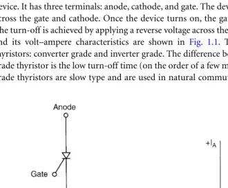
The thyristor, also called a silicon-controlled rectifier (SCR), is basically a four-layer three-junction pnpn
device. It has three terminals: anode, cathode, and gate. The device is turned on by applying a short pulse across the gate and cathode. Once the device turns on, the gate loses its control to turn off the device. The turn-off is achieved by applying a reverse voltageacross the anode and cathode. The thyristor symbol and its volt–ampere characteristics are shown in Fig. 1.1. There are basically two classifications of thyristors: converter grade and inverter grade. The difference between a converter-grade and an inverter-grade thyristor is the low turn-off time (on the order of a few microseconds) for the latter. The converter-grade thyristors are slow type and are used in natural commutation (or phase-controlled) applications.
Inverter-grade thyristors are used in forced commutation applications such as DC-DC choppers and DC-AC inverters. The inverter-grade thyristors are turned off by forcing the current to zero using an external commutation circuit. This requires additional commutating components, thus resulting in additional losses in the inverter.
Thyristors are highly rugged devices in terms of transient currents, di/dt, and dv/dt capability. The forward voltage drop in thyristors is about 1.5 to 2 V, and even at higher currents of the order of 1000 A, it seldom exceeds 3 V. While the forward voltage determines the on-state power loss of the device at any given current, the switching power loss becomes a dominating factor affecting the device junction temperature at high operating frequencies. Because of this, the maximum switching frequencies possible using thyristors are limited in comparison with other power devices considered in this section.
Thyristors have I2t withstand capability and can be protected by fuses. The nonrepetitive surge current capability for thyristors is about 10 times their rated root mean square (rms) current. They must be protected by snubber networks for dv/dt and di/dt effects. If the specified dv/dt is exceeded, thyristors may start conducting without applying a gate pulse. In DC-to-AC conversion applications, it is necessary to use an antiparallel diode of similar rating across each main thyristor. Thyristors are available up to 6000 V, 3500 A. A triac is functionally a pair of converter-grade thyristors connected in antiparallel. The triac symbol and volt–ampere characteristics are shown in Fig. 1.2. Because of the integration, the triac has poor reapplied
dv/dt, poor gate current sensitivity at turn-on, and longer turn-off time. Triacs are mainly used in phase control applications such as in AC regulators for lighting and fan control and in solid-state AC relays.
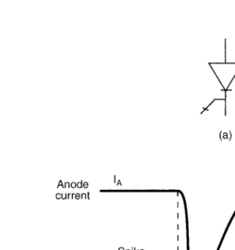
Gate Turn-Off Thyristor
The GTO is a power switching device that can be turned on by a short pulse of gate current and turned off by a reverse gate pulse. This reverse gate current amplitude is dependent on the anode current to be turned off. Hence there is no need for an external commutation circuit to turn it off. Because turn-off is provided by bypassing carriers directly to the gate circuit, its turn-off time is short, thus giving it more capability for high-frequency operation than thyristors. The GTO symbol and turn-off characteristics are shown in Fig. 1.3.
GTOs have the I2t withstand capability and hence can be protected by semiconductor fuses. For reliable operation of GTOs, the critical aspects are proper design of the gate turn-off circuit and the snubber circuit. A GTO has a poor turn-off current gain of the order of 4 to 5. For example, a 2000-A peak current
Reverse-Conducting Thyristor (RCT) and Asymmetrical
Silicon-Controlled Rectifier (ASCR)
Normally in inverter applications, a diode in antiparallel is connected to the thyristor for commu-tation/freewheeling purposes. In RCTs, the diode is integrated with a fast switching thyristor in a single silicon chip. Thus, the number of power devices could be reduced. This integration brings forth a substantial improvement of the static and dynamic characteristics as well as its overall circuit performance.
The RCTs are designed mainly for specific applications such as traction drives. The antiparallel diode limits the reverse voltage across the thyristor to 1 to 2 V. Also, because of the reverse recovery behavior of the diodes, the thyristor may see very high reapplied dv/dt when the diode recovers from its reverse voltage. This necessitates use of large RCsnubber networks to suppress voltage transients. As the range of application of thyristors and diodes extends into higher frequencies, their reverse recovery charge becomes increasingly important. High reverse recovery charge results in high power dissipation during switching.
The ASCR has similar forward blocking capability to an inverter-grade thyristor, but it has a limited reverse blocking (about 20 to 30 V) capability. It has an on-state voltage drop of about 25% less than an inverter-grade thyristor of a similar rating. The ASCR features a fast turn-off time; thus it can work at a higher frequency than an SCR. Since the turn-off time is down by a factor of nearly 2, the size of the commutating components can be halved. Because of this, the switching losses will also be low.
Gate-assisted turn-off techniques are used to even further reduce the turn-off time of an ASCR. The application of a negative voltage to the gate during turn-off helps to evacuate stored charge in the device and aids the recovery mechanisms. This will, in effect, reduce the turn-off time by a factor of up to 2
Power Transistor
Power transistors are used in applications ranging from a few to several hundred kilowatts and switching frequencies up to about 10 kHz. Power transistors used in power conversion applications are generally
npn type. The power transistor is turned on by supplying sufficient base current, and this base drive has to be maintained throughout its conduction period. It is turned off by removing the base drive and making the base voltage slightly negative (within –VBE(max)). The saturation voltage of the device is normally 0.5 to 2.5 V and increases as the current increases. Hence, the on-state losses increase more than proportionately with current. The transistor off-state losses are much lower than the on-state losses because the leakage current of the device is of the order of a few milliamperes. Because of relatively larger switching times, the switching loss significantly increases with switching frequency. Power transistors can block only forward voltages. The reverse peak voltage rating of these devices is as low as 5 to 10 V.
Power transistors do not have I2t withstand capability. In other words, they can absorb only very little energy before breakdown. Therefore, they cannot be protected by semiconductor fuses, and thus an electronic protection method has to be used.
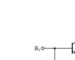
To eliminate high base current requirements, Darlington configurations are commonly used. They are available in monolithic or in isolated packages. The basic Darlington configuration is shown schematically in Fig. 1.4. The Darlington configuration presents a specific advantage in that it can considerably increase the current switched by the transistor for a given base drive. The VCE(sat) for the Darlington is generally more than that of a single transistor of similar rating with corresponding increase in on-state power loss. During switching, the reverse-biased collector junction may show hot-spot breakdown effects that are specified by reverse-bias safe operating area (RBSOA) and forward-bias safe operating area (FBSOA). Modern devices with highly interdigited emitter base geometry force more uniform current distribution and therefore considerably improve secondary breakdown effects. Normally, a well-designed switching aid network constrains the device operation well within the SOAs.
Power MOSFET
Power MOSFETs are marketed by different manufacturers with differences in internal geometry and with different names such as MegaMOS, HEXFET, SIPMOS, and TMOS. They have unique features that make them potentially attractive for switching applications. They are essentially voltage-driven rather than current-driven devices, unlike bipolar transistors.
The gate of a MOSFET is isolated electrically from the source by a layer of silicon oxide. The gate draws only a minute leakage current on the order of nanoamperes. Hence, the gate drive circuit is simple and power loss in the gate control circuit is practically negligible. Although in steady state the gate draws
capacitances have to be charged and discharged appropriately to obtain the desired switching speed, and the drive circuit must have a sufficiently low output impedance to supply the required charging and discharging currents. The circuit symbol of a power MOSFET is shown in Fig. 1.5.
Power MOSFETs are majority carrier devices, and there is no minority carrier storage time. Hence, they have exceptionally fast rise and fall times. They are essentially resistive devices when turned on, while bipolar transistors present a more or less constant VCE(sat) over the normal operating range. Power dissipation in MOSFETs is Id2RDS(on), and in bipolars it is ICVCE(sat). At low currents, therefore, a power MOSFET may have a lower conduction loss than a comparable bipolar device, but at higher currents, the conduction loss will exceed that of bipolars. Also, the RDS(on) increases with temperature.
An important feature of a power MOSFET is the absence of a secondary breakdown effect, which is present in a bipolar transistor, and as a result, it has an extremely rugged switching performance. In MOSFETs, RDS(on) increases with temperature, and thus the current is automatically diverted away from the hot spot. The drain body junction appears as an antiparallel diode between source and drain. Thus, power MOSFETs will not support voltage in the reverse direction. Although this inverse diode is relatively fast, it is slow by comparison with the MOSFET. Recent devices have the diode recovery time as low as 100 ns. Since MOSFETs cannot be protected by fuses, an electronic protection technique has to be used. With the advancement in MOS technology, ruggedized MOSFETs are replacing the conventional MOSFETs. The need to ruggedize power MOSFETs is related to device reliability. If a MOSFET is operating within its specification range at all times, its chances for failing catastrophically are minimal. However, if its absolute maximum rating is exceeded, failure probability increases dramatically. Under actual operating conditions, a MOSFET may be subjected to transients—either externally from the power bus supplying the circuit or from the circuit itself due, for example, to inductive kicks going beyond the absolute maximum ratings. Such conditions are likely in almost every application, and in most cases are beyond a designer’s control. Rugged devices are made to be more tolerant for overvoltage transients. Ruggedness is the ability of a MOSFET to operate in an environment of dynamic electrical stresses, without activating any of the parasitic bipolar junction transistors. The rugged device can withstand higher levels of diode recovery dv/dt and static dv/dt.
Insulated-Gate Bipolar Transistor (IGBT)
The IGBT has the high input impedance and high-speed characteristics of a MOSFET with the conductivity characteristic (low saturation voltage) of a bipolar transistor. The IGBT is turned on by applying a positive
The structure of an IGBT is more like a thyristor and MOSFET. For a given IGBT, there is a critical value of collector current that will cause a large enough voltage drop to activate the thyristor. Hence, the device manufacturer specifies the peak allowable collector current that can flow without latch-up occurring. There is also a corresponding gate source voltage that permits this current to flow that should not be exceeded.
Like the power MOSFET, the IGBT does not exhibit the secondary breakdown phenomenon common to bipolar transistors. However, care should be taken not to exceed the maximum power dissipation and specified maximum junction temperature of the device under all conditions for guaranteed reliable operation. The on-state voltage of the IGBT is heavily dependent on the gate voltage. To obtain a low on-state voltage, a sufficiently high gate voltage must be applied.
In general, IGBTs can be classified as punch-through (PT) and nonpunch-through (NPT) structures, as shown in Fig. 1.6. In the PT IGBT, an N+ buffer layer is normally introduced between the P+ substrate and the N− epitaxial layer, so that the whole N− drift region is depleted when the device is blocking the off-state voltage, and the electrical field shape inside the N− drift region is close to a rectangular shape. Because a shorter N− region can be used in the punch-through IGBT, a better trade-off between the forward voltage drop and turn-off time can be achieved. PT IGBTs are available up to about 1200 V.
High-voltage IGBTs are realized through a nonpunch-through process. The devices are built on an N− wafer substrate which serves as the N− base drift region. Experimental NPT IGBTs of up to about 4 kV have been reported in the literature. NPT IGBTs are more robust than PT IGBTs, particularly under short circuit conditions. But NPT IGBTs have a higher forward voltage drop than the PT IGBTs.
The PT IGBTs cannot be as easily paralleled as MOSFETs. The factors that inhibit current sharing of parallel-connected IGBTs are (1) on-state current unbalance, caused by VCE(sat) distribution and main circuit wiring resistance distribution, and (2) current unbalance at turn-on and turn-off, caused by the
MOS-Controlled Thyristor (MCT)
The MCT is a new type of power semiconductor device that combines the capabilities of thyristor voltage and current with MOS gated turn-on and turn-off. It is a high-power, high-frequency, low-conduction drop and a rugged device, which is more likely to be used in the future for medium and high power applications. A cross-sectional structure of a p-type MCT with its circuit schematic is shown in Fig. 1.7. The MCT has a thyristor type structure with three junctions and pnpn layers between the anode and cathode. In a practical MCT, about 100,000 cells similar to the one shown are paralleled to achieve the desired current rating. MCT is turned on by a negative voltage pulse at the gate with respect to the anode, and is turned off by a positive voltage pulse.
The MCT was announced by the General Electric R&D Center on November 30, 1988. Harris Semiconductor Corporation has developed two generations of p-MCTs. Gen-1 p-MCTs are available at 65 A/1000 V and 75 A/600 V with peak controllable current of 120 A. Gen-2 p-MCTs are being developed at similar current and voltage ratings, with much improved turn-on capability and switching speed. The reason for developing a p-MCT is the fact that the current density that can be turned off is two or three times higher than that of an n-MCT; but n-MCTs are the ones needed for many practical applications.
The advantage of an MCT over IGBT is its low forward voltage drop. n-type MCTs will be expected to have a similar forward voltage drop, but with an improved reverse bias safe operating area and switching speed. MCTs have relatively low switching times and storage time. The MCT is capable of high current densities and blocking voltages in both directions. Since the power gain of an MCT is extremely high, it could be driven directly from logic gates. An MCT has high di/dt (of the order of 2500 A/µs) and high
dv/dt (of the order of 20,000 V/µs) capability.
The MCT, because of its superior characteristics, shows a tremendous possibility for applications such as motor drives, uninterrupted power supplies, static VAR compensators, and high power active power line conditioners.
The current and future power semiconductor devices developmental direction is shown in Fig. 1.8. High-temperature operation capability and low forward voltage drop operation can be obtained if silicon is replaced by silicon carbide material for producing power devices. The silicon carbide has a higher band gap than silicon. Hence, higher breakdown voltage devices could be developed. Silicon carbide devices
References
Bose, B.K., Modern Power Electronics: Evaluation, Technology, and Applications, IEEE Press, New York, 1992. Harris Semiconductor, User’s Guide of MOS Controlled Thyristor.
Huang, A.Q., Recent developments of power semiconductor devices, in VPEC Seminar Proceedings,
September 1995, 1–9.
Mohan, N. and T. Undeland, Power Electronics: Converters, Applications, and Design, John Wiley & Sons, New York, 1995.
Wojslawowicz, J., Ruggedized transistors emerging as power MOSFET standard-bearers, Power Technics Magazine, January 1988, 29–32.
Further Information
Bird, B.M. and K.G. King, An Introduction to Power Electronics, Wiley-Interscience, New York, 1984. Sittig, R. and P. Roggwiller, Semiconductor Devices for Power Conditioning, Plenum, New York, 1982. Temple, V.A.K., Advances in MOS controlled thyristor technology and capability, Power Conversion,
544–554, Oct. 1989.
Williams, B.W., Power Electronics, Devices, Drivers and Applications, John Wiley, New York, 1987.
1.2 Diodes
Sohail Anwar
Power diodes play an important role in power electronics circuits. They are mainly used as uncontrolled rectifiers to convert single-phase or three-phase AC voltage to DC. They are also used to provide a path for the current flow in inductive loads. Typical types of semiconductor materials used to construct diodes are silicon and germanium. Power diodes are usually constructed using silicon because silicon diodes can operate at higher current and at higher junction temperatures than germanium diodes. The symbol for a semiconductor diode is given in Fig. 1.9. The terminal voltage and current are represented as Vd and Id, respectively. Figure 1.10 shows the structure of a diode. It has an anode (A) terminal and a cathode (K) terminal. The diode is constructed by joining together two pieces of semiconductor material—a p-type and an n-type—to form a pn-junction. When the anode terminal is positive with respect to the cathode terminal, the pn-junction becomes forward-biased and the diode conducts current with a relatively low voltage drop. When the cathode terminal is positive with respect to the anode terminal, the pn-junction
Characteristics
The voltage-current characteristics of a diode are shown in Fig. 1.11. In the forward region, the diode starts conducting as the anode voltage is increased with respect to the cathode. The voltage where the current starts to increase rapidly is called the knee voltage of the diode. For a silicon diode, the knee voltage is approximately 0.7 V. Above the knee voltage, small increases in the diode voltage produce large increases in the diode current. If the diode current is too large, excessive heat will be generated, which can destroy the diode. When the diode is reverse-biased, diode current is very small for all values of reverse voltage less than the diode breakdown voltage. At breakdown, the diode current increases rapidly for small increases in diode voltage.
Principal Ratings for Diodes
Figures 1.12 and 1.13 show typical data sheets for power diodes. Maximum Average Forward Current
The maximum average forward current (If(avg)max)is the current a diode can safely handle when forward biased. Power diodes are available in ratings from a few amperes to several hundred amperes. For example, the power diode D6 described in the data specification sheet (Fig 1.12) can handle up to 6 A in the forward direction when used as a rectifier. Peak Inverse Voltage
The peak inverse voltage (PIV) of a diode is the maximum reverse voltage that can be connected across a diode without breakdown. The peak inverse voltage is also called peak reverse voltage or reverse breakdown voltage. The PIV ratings of power diodes extend from a few volts to several thousand volts. For example, the power diode D6 has a PIV rating of up to 1600 V, as shown in Fig. 1.12.
FIGURE 1.9 Diode symbol. Id
Vd +
_ A
K
FIGURE 1.10 Diode structure.
I
dV
d+
_
A
Maximum Surge Current
The IFSM (forward surge maximum) rating is the maximum current that the diode can handle as an occasional transient or from a circuit fault. The IFSM rating for the power diode D6 is up to 190 A, as shown in Fig 1.12.
Maximum Junction Temperature
This parameter defines the maximum junction temperature that a diode can withstand without failure. The maximum junction temperature for the power diode D6 is 180°C.
Rectifier Circuits
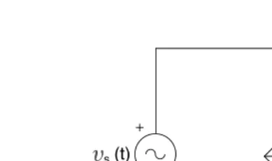
Rectifier circuits produce a DC voltage or current from an AC source. The diode is an essential component of these circuits. Figure 1.14 shows a half-wave rectifier circuit using a diode. During the positive half cycle of the source voltage, the diode is forward-biased and conducts for vs(t) > Ef. The value of Ef for germanium is 0.2 V and for silicon it is 0.7 V. During the negative half cycle of vs(t) , the diode is reverse-biased and does not conduct. The voltage vL(t) across the load RL is shown in Fig. 1.15.
The half-wave rectifier circuit produces a pulsating direct current that uses only the positive half cycle of the source voltage. The full-wave rectifier shown in Fig. 1.16 uses both half cycles of source voltage. During the positive half cycle of vs(t), diodes D1 and D2 are forward-biased and conduct. Diodes D3 and D4 are reverse-biased and do not conduct. During the negative half cycle of vs(t), diodes D1 and D2 are
FIGURE 1.14 Basic circuit for half-wave rectifier.
FIGURE 1.15 Input and output voltage waveforms for the circuit in Fig. 1.14.
Testing a Power Diode
An ohmmeter can be used to test power diodes. The ohmmeter is connected so that the diode is forward-biased. This should give a low resistance reading. Reversing the ohmmeter leads should give a very high resistance or even an infinite reading. A very low resistance reading in both directions indicates a shorted diode. A high resistance reading in both directions indicates an open diode.
Protection of Power Diodes
A power diode must be protected against over current, over voltage, and transients.
When a diode is reverse-biased, it acts like an open circuit. If the reverse bias voltage exceeds the breakdown voltage, a large current flow results. With this high voltage and large current, power dissipation at the diode junction may exceed its maximum value, destroying the diode. For the diode protection, it is a usual practice to choose a diode with a peak reverse voltage rating that is 1.2 times higher than the expected voltage during normal operating conditions.
Current ratings for diodes are based on the maximum junction temperatures. As a safety precaution, it is recommended that the diode current be kept below this rated value. Electrical transients can cause higher-than-normal voltages across a diode. To protect a diode from the transients, an RC series circuit
FIGURE 1.16 Basic circuit for full-wave rectifier.
FIGURE 1.17 Input and output voltage waveforms for the circuit in Fig. 1.16.
D1
D2 D3
D4
(t)s
Iload
V
1.3 Schottky Diodes
Sohail Anwar
Bonding a metal, such as aluminum or platinum, to n-type silicon forms a Schottky diode. The Schottky diode is often used in integrated circuits for speed switching applications. An example of a high-speed switching application is a detector at microwave frequencies. The Schottky diode has a voltage-current characteristic similar to that of a silicon pn-junction diode. The Schottky is a subgroup of the TTL family and is designed to reduce the propagation delay time of the standard TTL IC chips. The construction of the Schottky diode is shown in Fig. 1.18a, and its symbol is shown in Fig. 1.18b.
Characteristics
The low-noise characteristics of the Schottky diode make it ideal for application in power monitors of low-level radio frequency, detectors for high frequency, and Doppler radar mixers. One of the main advantages of the Schottky barrier diode is its low forward voltage drop compared with that of a silicon diode. In the reverse direction, both the breakdown voltage and the capacitance of a Schottky barrier diode behave very much like those of a one-sided step junction. In the one-sided step junction, the doping level of the semiconductor determines the breakdown voltage. Because of the finite radius at the edges of the diode and because of its sensitivity to surface cleanliness, the breakdown voltage is always somewhat lower than theoretical predictions.
Data Specifications
The data specification sheet for a DSS 20-0015B power Schottky diode is provided as an example in
Figs. 1.19 and 1.20. Specifications will vary depending on the application and model of Schottky diode.
Testing of Schottky Diodes
Two ways of testing the diodes use either a voltmeter or a digital multimeter. The voltmeter should be set to the low resistance scale. A single diode or rectifier should read a low resistance, typically, 2/3 scale from the resistance in the forward direction. In the reverse direction, the resistance should be nearly infinite. It should not read near 0 Ω in the shorted or open directions. The diode will result in a higher
K
A
A K
p-type substrate SiO2
Metallic
n-type n +
FIGURE 1.19 Data specification sheet for a DSS 20-00105B power Schottky diode (front). (Courtesy of IXYS.)
Power Schottky Rectifier
Features
¥ International standard package Very low VF
Extremely low switching losses Low IRM-values
Epoxy meets UL 94V-0
Applications
Rectifiers in switch mode power supplies (SMPS)
Free wheeling diode in low voltage converters
Advantages
High reliability circuit operation Low voltage peaks for reduced protection circuits
Low noise switching Low losses
Dimensions see outlines.pdf
Pulse test: Pulse Width = 5 ms, Duty Cycle < 2.0 %
Data according to IEC 60747 and per diode unless otherwise specified
IXYS reserves the right to change limits, Conditions and dimensions.
A C
C A TO-220 AC
C (TAB)
A = Anode, C = Cathode , TAB = Cathode
Symbol Conditions Maximum Ratings
IFRMS 35 A
IFAVM TC = 135 C; rectangular, d = 0.5 20 A
IFSM TVJ = 45¡C; tp = 10 ms (50 Hz), sine 350 A
EAS IAS = tbd A; L = 180 H; TVJ = 25¡C; non repetitive tbd mJ
IAR VA =1.5 VRRM typ.; f=10 kHz; repetitive tbd A
(dv/dt)cr tbd V/ s
TVJ -55...+150 C
TVJM 150 C
Tstg -55...+150 C
Ptot TC = 25 C 9 0 W
Md mounting torque 0.4...0.6 Nm
Weight typical 2 g
IFAV = 20 A VRRM = 15 V VF = 0.33 V
VRSM VRRM Type
V V
15 15 DSS 20-0015B
Symbol Conditions Characteristic Values typ. max.
IR TVJ = 25¡C VR = VRRM 10 mA
TVJ = 100¡C VR = VRRM 200 mA
VF IF = 20 A; TVJ = 125¡C 0.33 V
IF = 20 A; TVJ = 25¡C 0.45 V
IF = 40 A; TVJ = 125 ¡C 0.43 V
RthJC 1.4 K/W
RthCH 0.5 K/W
scale reading of resistance as a result of its lower voltage drop. What is being measured is the resistance at a particular low current point; it is not the actual resistance in a power rectifier circuit.
The digital multimeter will usually have a diode test mode. When using this mode, a silicon diode should read between 0.5 to 0.8 V in the forward direction and open in the reverse direction. A germanium diode will be in the range of 0.2 to 0.4 V in the forward direction. By using the normal resistance range,
FIGURE 1.20 Data specification sheet for a DSS 20-00105B power Schottky diode (reverse). 0.0 0.2 0.4 0.6
1 10 100
0 2 4 6 8 10 12 14 0.1
1 10 100 1000
5 15 25
0 10 20
0 2 4 6 8 10 12 14
0.0001 0.001 0.01 0.1 1 10
0.01 0.1 1
0 40 80 120 160 0 10 20 30 40 IF(AV) TC ¡C IF(AV) t s K/W 00 10000 tP 0 2 4 6 8 10 12 14 100 1000 10000 CT IR IF A
VF VR VR
V pF V mA A P(AV) W ZthJC V Single Pulse 2 DSS 20-0015B A s TVJ=150¡C
125¡C
100¡C
75¡C
25¡C TVJ =
150¡C 125¡C 25¡C
TVJ= 25¡C
d=0.5 d = DC 0.5 0.33 0.25 0.17 0.08 0.08 D=0.5 0.17 DC 50¡C 0.33 0.25
Fig. 3 Typ. junction capacitance CT versus reverse voltage VR Fig. 2 Typ. value of reverse current IR
versus reverse voltage VR Fig. 1 Maximum forward voltage
drop characteristics
Fig. 4 Average forward current IF(AV)
versus case temperature TC
Fig. 5 Forward power loss characteristics
30 10010 100 10 1000
10000
1.4 Thyristors
Sohail Anwar
Thyristors are four-layer pnpn power semiconductor devices. These devices switch between conducting and nonconducting states in response to a control signal. Thyristors are used in timing circuits, AC motor speed control, light dimmers, and switching circuits. Small thyristors are also used as pulse sources for large thyristors. The thyristor family includes the silicon-controlled rectifier (SCR), the DIAC, the Triac, the silicon-controlled switch (SCS), and the gate turn-off thyristor (GTO).
The Basics of Silicon-Controlled Rectifiers (SCR)
The SCR is the most commonly used electrical power controller. An SCR is sometimes called a pnpn
diode because it conducts electrical current in only one direction. Figure 1.21a shows the SCR symbol. It has three terminals: the anode (A), the cathode (K), and the gate (G). The anode and the cathode are the power terminals and the gate is the control terminal. The structure of an SCR is shown in
Fig. 1.21b.
When the SCR is forward-biased, that is, when the anode of an SCR is made more positive with respect to the cathode, the two outermost pn-junctions are forward-biased. The middle pn-junction is reverse-biased and the current cannot flow. If a small gate current is now applied, it forward-biases the middle pn -junction and allows a much larger current to flow through the device. The SCR stays ON even if the gate current is removed. SCR shutoff occurs only when the anode current becomes less than a level called the holding current (IH).
Characteristics
The volt-ampere characteristic of an SCR is shown in Fig. 1.22. If the forward bias is increased to the forward breakover voltage, VFBO, the SCR turns ON. The value of forward breakover voltage is controlled by the gate current IG. If the gate-cathode pn-junction is forward-biased, the SCR is turned ON at a lower breakover voltage than with the gate open. As shown in Fig. 1.22, the breakover voltage decreases with an increase in the gate current. At a low gate current, the SCR turns ON at a lower forward anode voltage. At a higher gate current, the SCR turns ON at a still lower value of forward anode voltage.
When the SCR is reverse-biased, there is a small reverse leakage current (IR). If the reverse bias is increased until the voltage reaches the reverse breakdown voltage (V(BR)R), the reverse current will increase sharply. If the current is not limited to a safe value, the SCR may be destroyed.
G
K A
(anode)
(cathode) (gate)
SCR Turn-Off Circuits
If an SCR is forward-biased and a gate signal is applied, the device turns ON. Once the anode current is above I , the gate loses control. The only way to turn OFF the SCR is to make the anode terminal negative
FIGURE 1.22 SCR characteristics.
FIGURE 1.23 An SCR turn-off circuit.
Holding current (I )
+ I
+ V
Forward conduction region (on state)
Forward blocking region (off state)
Forward breakover voltage (VFBO)
Reverse blocking region Reverse leakage current (IR)
Maximum reverse voltage (V(BR)R)
Reverse breakdown
I > I > I
G2
I I
G1 G0
I
G 2 G1 G 0
A
A
- I
A K
- V
H
AC line commutation. The load current IL flows during the positive half cycle of the source voltage. The SCR is reverse-biased during the negative half cycle of the source voltage. With a zero gate current, the SCR will turn OFF if the turn-off time of the SCR is less than the duration of the half cycle.
SCR Ratings
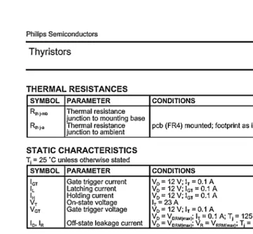
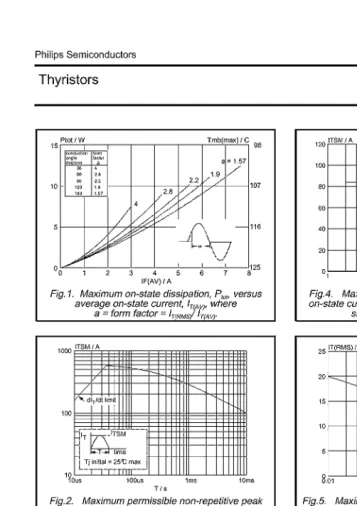
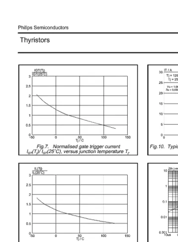
A data sheet for a typical thyristor follows this section and includes the following information:
Surge Current Rating (IFM)—The surge current rating (IFM) of an SCR is the peak anode current an SCR can handle for a short duration.
Latching Current (IL)—A minimum anode current must flow through the SCR in order for it to stay ON initially after the gate signal is removed. This current is called the latching current (IL).
Holding Current (IH)—After the SCR is latched on, a certain minimum value of anode current is needed to maintain conduction. If the anode current is reduced below this minimum value, the SCR will turn OFF.
Peak Repetitive Reverse Voltage (VRRM)—The maximum instantaneous voltage that an SCR can with-stand, without breakdown, in the reverse direction.
Peak Repetitive Forward Blocking Voltage (VDRM)—The maximum instantaneous voltage that the SCR can block in the forward direction. If the VDRM rating is exceeded, the SCR will conduct without a gate voltage.
Nonrepetitive Peak Reverse Voltage (VRSM)—The maximum transient reverse voltage that the SCR can withstand.
Maximum Gate Trigger Current (IGTM)—The maximum DC gate current allowed to turn the SCR ON.
Minimum Gate Trigger Voltage (VGT)—The minimum DC gate-to-cathode voltage required to trigger the SCR.
Minimum Gate Trigger Current (IGT)—The minimum DC gate current necessary to turn the SCR ON.
The DIAC
A DIAC is a three-layer, low-voltage, low-current semiconductor switch. The DIAC symbol is shown in
Fig. 1.24a. The DIAC structure is shown in Fig. 1.24b. The DIAC can be switched from the OFF to the ON state for either polarity of applied voltage.
The volt-ampere characteristic of a DIAC is shown in Fig. 1.25. When Anode 1 is made more positive than Anode 2, a small leakage current flows until the breakover voltage VBO is reached. Beyond VBO, the
A n o d e 1
A n o d e 2
(a)
N
P
P
N
N
Anode 2 Anode 1
1
2
2 1
3
DIAC will conduct. When Anode 2 is made more positive relative to Anode 1, a similar phenomenon occurs. The breakover voltages for the DIAC are almost the same in magnitude in either direction. DIACs are commonly used to trigger larger thyristors such as SCRs and Triacs.
The Triac
The Triac is a three-terminal semiconductor switch. It is triggered into conduction in both the forward and the reverse directions by a gate signal in a manner similar to the action of an SCR. The Triac symbol is shown in Fig. 1.26a and the Triac structure is shown in Fig. 1.26b.
The volt-ampere characteristic of the Triac is shown in Fig. 1.27. The breakover voltage of the Triac can be controlled by the application of a positive or negative signal to the gate. As the magnitude of the gate signal increases, the breakover voltage decreases. Once the Triac is in the ON state, the gate signal can be removed and the Triac will remain ON until the main current falls below the holding current (IH) value.
The Silicon-Controlled Switch
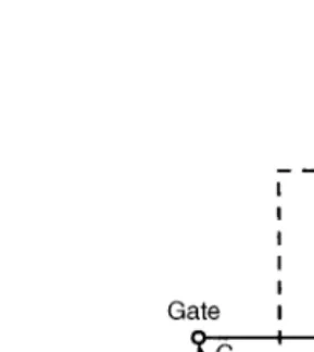
The SCS is a four-layer pnpn device. The SCS symbol is shown in Fig. 1.28a and the SCS structure is shown in Fig. 1.28b. The SCS has two gates labeled as the anode gate (AG) and the cathode gate (KG). An SCS can be turned ON by the application of a negative gate pulse at the anode gate. When the SCS
FIGURE 1.25 The DIAC characteristics.
FIGURE 1.26 (a) The Triac symbol; (b) the Triac structure.
I
V
BO
V
BO
V
BR
I
BR
I
M T 2
G
M T
1
(a)
N
P P
N
N N
N
Gate MT2
MT1
The Gate Turn-Off Thyristor
The GTO is a power semiconductor switch that turns ON by a positive gate signal. It can be turned OFF by a negative gate signal. The GTO symbol is shown in Fig. 1.29a and the GTO structure is shown in
Fig. 1.29b. The GTO voltage and current ratings are lower than those of SCRs. The GTO turn-off time is lower than that of SCR. The turn-on time is the same as that of an SCR.
Data Sheet for a Typical Thyristor
FIGURE 1.27 The Triac characteristics.
FIGURE 1.28 (a) The SCS symbol; (b) the SCS structure.
FIGURE 1.29 (a) The GTO symbol; (b) the GTO structure.
I
V
BR
V
I
HBR
V
H
I
Main Terminal 2 (negative)
Main Terminal (positive)
A
K
AG
KG
(a)
Anode (A)
Cathode (K)
Anode Gate (AG) Cathode Gate
(KG)
(b)
A
K
G
(a)
Anode
Cathode Gate
1.5 Power Bipolar Junction Transistors
Sohail Anwar
Power bipolar junction transistors (BJTs) play a vital role in power circuits. Like most other power devices, power transistors are generally constructed using silicon. The use of silicon allows operation of a BJT at higher currents and junction temperatures, which leads to the use of power transistors in AC applications where ranges of up to several hundred kilowatts are essential.
The power transistor is part of a family of three-layer devices. The three layers or terminals of a transistor are the base, the collector, and the emitter. Effectively, the transistor is equivalent to having two pn-diode junctions stacked in opposite directions to each other. The two types of a transistor are termed npn and
pnp. The npn-type transistor has a higher current-to-voltage rating than the pnp and is preferred for most power conversion applications. The easiest way to distinguish an npn-type transistor from a pnp-type is by virtue of the schematic or circuit symbol. The pnp type has an arrowhead on the emitter that points toward the base. Figure 1.36 shows the structure and the symbol of a pnp-type transistor. The npn-type transistor has an arrowhead pointing away from the base. Figure 1.37 shows the structure and the symbol of an npn-type transistor.
When used as a switch, the transistor controls the power from the source to the load by supplying sufficient base current. This small current from the driving circuit through the base–emitter, which must be maintained, turns on the collector—emitter path. Removing the current from the base–emitter path and making the base
The Volt-Ampere Characteristics of a BJT
The volt-ampere characteristics of a BJT are shown in Fig. 1.38. Power transistors have exceptional characteristics as an ideal switch and they are primarily used as switches. In this type of application, they make use of the common emitter connection shown in Fig. 1.39. The three regions of operation for a transistor that must be taken into consideration are the cutoff, saturation, and the active region. When the base current (IB) is zero, the collector current (IC) is insignificant and the transistor is driven into the cutoff region. The transistor is now in the OFF state. The collector–base and base–emitter junctions are reverse-biased in the cutoff region or OFF state, and the transistor behaves as an open switch. The base current (IB) determines the saturation current. This occurs when the base current is sufficient to drive the transistor into saturation. During saturation, both junctions are forward-biased and the transistor acts like a closed switch. The saturation voltage increases with an increase in current and is normally between 0.5 to 2.5 V. The active region of the transistor is mainly used for amplifier applications and should be
FIGURE 1.36 pnp transistor structure (a) and circuit symbol (b).
FIGURE 1.37 npn transistor structure (a) and circuit symbol (b).
Collector
Base
Emitter
(a) (b)
P N P
E B
C
B
C
E IC
+ VCE
--lE
IB
Collector
Base
Emitter
BJT Biasing
When a transistor is used as a switch, the control circuit provides the necessary base current. The current of the base determines the ON or OFF state of the transistor switch. The collector and the emitter of the transistor form the power terminals of the switch.
The DC load line represents all of the possible operating points of a transistor and is shown in Fig. 1.40. The operating point is where the load line and the base current intersect and is determined by the values of VCC and RC.
In the ON state, the ideal operating point occurs when the collector current IC is equal to VCC/RC and
VCE is zero. The actual operating point occurs when the load line intersects the base current at the saturation point. This occurs when the base current equals the saturation current or IB = IB(sat). At this point, the collector current is maximum and the transistor has a small voltage drop across the collector–emitter terminals called the saturation voltage VCE(sat).
In the OFF state, or cutoff point, the ideal operating point occurs when the collector current IC is zero and the collector–emitter voltage VCE is equal to the supply voltage VCC. The actual operating point, in the OFF state, occurs when the load line intersects the base current (IB = 0). At the cutoff point, the collector current is the leakage current. By applying Kirchoff ’s voltage law around the output loop, the collector–emitter voltage (VCE) can be found.
The operating points between the saturation and cutoff constitute the active region. When operating
FIGURE 1.38 BJT V-I characteristic.
FIGURE 1.39 Biasing of a transistor.
Saturation voltage Vce(sat)
Active Region Saturation
(ON)
Cutoff (OFF) Leakage
current Ic
IC and collector–emitter voltage VCE. For satisfactory operation, a slightly higher than minimum base current will ensure a saturated ON state and will result in reduced turn-on time and power dissipation.
BJT Power Losses
The four types of transistor power losses are the ON-state and OFF-state losses and turn-ON and turn-OFF switching loss. OFF-state transistor losses are much lower than ON-state losses since the leakage current of the device is within a few milliamps. Essentially, when a transistor is in the off state, whatever the value of collector–emitter voltage, there is no collector current. Switching losses depend on switching frequency. The highest possible switching frequency of the transistor is limited by the losses due to the rate of switching. In other words, the higher the switching frequency, the more power loss in the transistor.
BJT Testing
Testing of the state of a transistors can be done with a multimeter. When a transistor is forward-biased, the base–collector and base–emitter regions should have a low resistance. When reverse-biased, the base– collector and base–emitter regions should have a high resistance. When testing the resistance between the collector and the emitter, the resistance reading should result in a much higher than forward bias base–collector and base–emitter resistance. However, faulty power transistors can appear shorted when measuring resistance across the collector and emitter, but still pass both junction tests.
BJT Protection
Transistors must be protected against high currents and voltages to prevent damage to the device. Since they are able to absorb very little energy before breakdown, semiconductor fuses cannot protect them. Thermal conditions are vitally important and can occur during high-frequency switching. Some of the most common types of BJT protection are overcurrent and overvoltage protection. Electronic protection techniques are also frequently used to provide needed protection for transistors.
Overcurrent protection turns the transistor OFF when the collector–emitter voltage and collector current reach a preset value. When the transistor is in the ON state, an increase in collector–emitter voltage causes an increase in the collector current and therefore an increase in junction temperature. Since the BJT has a negative temperature coefficient, the increase in temperature causes a decrease in resistance and results in an even higher collector current. This condition, called positive feedback, could eventually lead to thermal runaway and destroy the transistor. One such method of overcurrent protection limits the base current during an external fault. With the base current limited, the device current will be
FIGURE 1.40 DC load line.
FIGURE 1.41 Typical data sheet for a power transistor (page 1). (From National Semiconductor. With permission.)
LM195/LM395
Ultra Reliable Power Transistors
General DescriptionThe LM195/LM395 are fast, monolithic power integrated cir-cuits with complete overload protection. These devices, which act as high gain power transistors, have included on the chip, current limiting, power limiting, and thermal over-load protection making them virtually impossible to destroy from any type of overload. In the standard TO-3 transistor power package, the LM195 will deliver load currents in ex-cess of 1.0A and can switch 40V in 500 ns.
The inclusion of thermal limiting, a feature not easily avail-able in discrete designs, provides virtually absolute protec-tion against overload. Excessive power dissipaprotec-tion or inad-equate heat sinking causes the thermal limiting circuitry to turn off the device preventing excessive heating. The LM195 offers a significant increase in reliability as well as simplifying power circuitry. In some applications, where protection is unusually difficult, such as switching regulators, lamp or solenoid drivers where normal power dissipation is low, the LM195 is especially advantageous.
The LM195 is easy to use and only a few precautions need be observed. Excessive collector to emitter voltage can stroy the LM195 as with any power transistor. When the de-vice is used as an emitter follower with low source
imped-ance, it is necessary to insert a 5.0k resistor in series with the base lead to prevent possible emitter follower oscilla-tions. Although the device is usually stable as an emitter fol-lower, the resistor eliminates the possibility of trouble without degrading performance. Finally, since it has good high fre-quency response, supply bypassing is recommended. For low-power applications (under 100 mA), refer to the LP395 Ultra Reliable Power Transistor.
The LM195/LM395 are available in the standard TO-3, Kovar TO-5, and TO-220 packages. The LM195 is rated for opera-tion from 55 C to +150 C and the LM395 from 0 C to +125 C.
Features n Internal thermal limiting n Greater than 1.0A output current n 3.0 A typical base current n 500 ns switching time n 2.0V saturation
n Base can be driven up to 40V without damage n Directly interfaces with CMOS or TTL n 100% electrical burn-in
Simplified Circuit
DS006009-1
1.0 Amp Lamp Flasher