1 INTRODUCTION
General Introduction
Problem Statement
Importance of the Study
Aim and Objectives
Scope and Limitation of the Study
Introduction
Literature Review
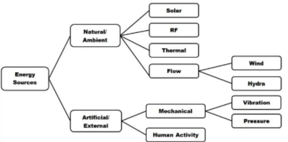
- Energy Harvesting Sources
- Mechanical Energy Harvester
- Thermal Energy Harvester
- Solar Energy Harvester
- Radiofrequency Harvester
- Summary of Energy Harvester
The energy conversion efficiency of a PV harvester depends on the cell efficiency and light intensity (Akhtar et al., 2015). The output waveform produced by the solar collector is highly dependent on the weather, the surface of the solar panel and the solar irradiance.
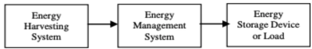
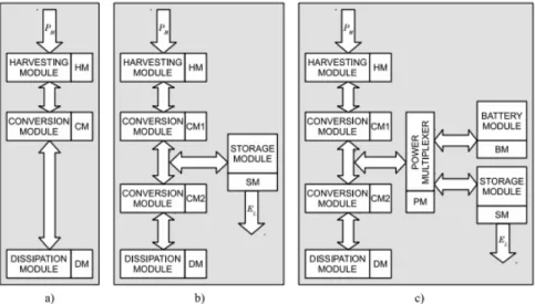
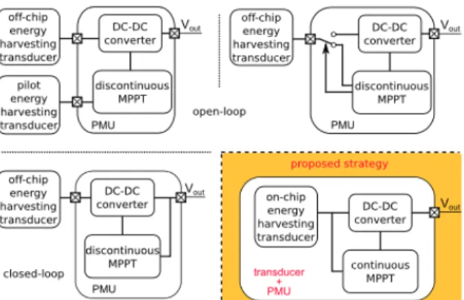
Power Management System
- Previous work on PMU Design
- Summary of Previous work on PMU Design
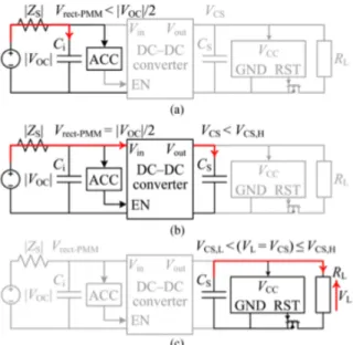
Shaltout argued that the proposed power management system design can be used not only to charge batteries, but also to power sensors when possible. The proposed system consists of several main components, including a full-wave rectifier, an analog control circuit, namely ACC, a DC-DC converter, a storage capacitor, and an energy sensing system. Due to the simplicity of the proposed circuit, this approach achieved an overall efficiency of 78% in most scenarios, and the power management circuit consumes only 5.16 μW during operation.
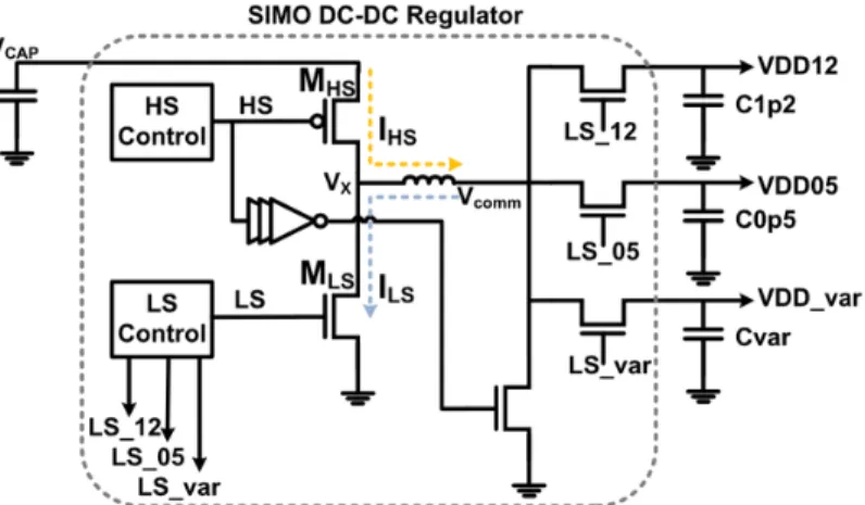
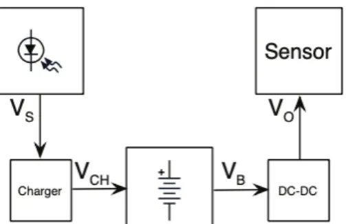
The proposed micro energy harvesting system has a very small form factor of 1.575 mm2 and consists of an auxiliary charge pump to increase the voltage level to meet the circuit requirements. Despite the small form factor, the design can handle input ranging from nW to μW. The block diagram of the proposed power management unit is shown in Figure 2.14 below. The proposed system can harvest energy from a solar cell with an input voltage of 0.38 V and supply 4 outputs at 4 different voltage levels.
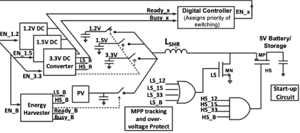
The only digital part in the proposed circuit was the power management unit as shown in the figure below. The voltage divider in the proposed system works as a reference to monitor the amount of voltage available at the primary storage.
Wireless Sensor Nodes
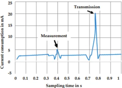
During the active mode, the node collects the vibration waveform and transmits it through the RF transmitter. Based on an experiment conducted in the study, the node consumes approximately 5 mA while measuring the vibration information and approximately 20 mA while transmitting the data to the base station.
Rectifiers
The proposed design is actually a modified version of the charge pump mentioned above using a transfer gate to produce a higher power output. Initially, when the AC signal is in a negative cycle, the VDS of NM1 is in the negative region, making it reverse biased and therefore off. 2018), by cascading several stages of the NMOS rectifier, a higher DC output voltage can be achieved.
However, since more stages are implemented in this design, the power loss due to diode power loss will be higher. In brief, rectifiers, as one of the important building blocks of the energy harvesting system, there are many different approaches to rectifier design. The key to designing a good rectifier for a power generation system is to design based on the required specifications, such as input voltage type and level.
The main problem of the conventional design is the finite threshold voltage of the transistors. This is a very crucial issue especially in ultra low power operation where the input signal is less than the threshold voltage of the devices.
Buck Converter
- Voltage Mode Control (VMC) vs Current Mode Control (CMC) In order to regulate the buck converter’s output voltage, there are two main types
- Pulse Width Modulation vs Pulse Frequency Modulation
- Previous work onn Buck Converter
For VCM, a type 3 compensator is required to improve the phase margin of the buck converter. An open loop buck converter controlled using pulse width modulation is shown in Figure 2.30 below. However, in an open-loop buck converter design, the output is not held constant since there is no feedback loop in the design.
Lu, et al., (2010) developed a voltage mode control buck converter using PWM techniques with 0.18μm CMOS technology. The proposed buck converter works with a digital error amplifier which allows a lower input voltage than other conventional buck converters. The design is claimed to have an efficiency of 90% under certain conditions where the input voltage is 1V and the generated output voltage is 0.5V. The figure below illustrates a simplified structure of the proposed voltage-mode control buck converter.
To further improve the efficiency of the PWM-controlled buck converter, Prateek, et al. 2014) proposed to reduce the large area overhead caused by the conventional helical inductors in the buck converter. She proposed replacing the conventional helical inductor with through-silicon-vias (TSV) inductors in a buck converter with PWM feedback.
System Specifications
Among all the types of energy harvesters discussed in Chapter 2, kinetic energy harvesting solutions are promising as they are able to provide sufficient energy by generating kinetic energy from vibrations of the passing train into electricity. In the study conducted by him, he simulated that the developed electromagnetic kinetic energy harvester can harvest up to an average of 29.3 mW.
Design Methodology
Work Plan
To know and adapt to the Mentor Graphics EDA tool (Silterra 0.13-μm CMOS process). However, in the middle of the project, the license for the Mentor Graphics EDA tool expired and it was replaced by Cadence Virtuoso (GPDK 45nm CMOS process). On the other hand, in the second part of the project, the signal waveform generated by the piezoelectric energy harvester was simulated using PWL source in Cadence Virtuoso.
Then the block designs like rectifier and buck converter were designed and constructed. Each of the block diagrams was divided into some smaller parts to make it easier to manage and design. A simplified flow diagram highlighting the workflow of Part 1 and Part 2 is also included in Figure 3.3.

Proposed PMU Design
Proposed Rectifier Design
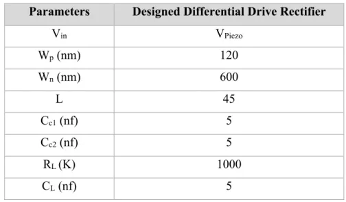
Various parameters such as circuit designs, W/L ratio of transistors, input and output loading will affect the power conversion efficiency (PCE) of the converter. The value of L for NMOS and PMOS transistors was chosen at the minimum length of the technology, which is 45 nm.
Proposed Buck Converter Design
- Sizing of Inductor and Capacitor
- Type 3 Compensator Values
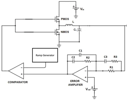
- Error Amplifier and Comparator
- Ramp Generator
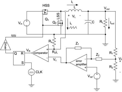
The PWM control technique is often implemented in buck converters as it is an effective control method which can improve the efficiency of the buck converter by monitoring the output voltage. The switching frequency of this buck converter was chosen to be 20 MHz to reduce the size of the filter, which comes mainly from the inductor and capacitor. A faster transient response can be achieved by simply increasing the converter's switching frequency.
However, higher switching frequency will lead to lower efficiency of the buck converter as the switching loss also increases. The size of the inductor and capacitor is therefore important, and it must be chosen wisely so that the buck converter can achieve a better PCE. The inductor size selected is a bit larger as larger size of inductor can improve the efficiency of the converter.
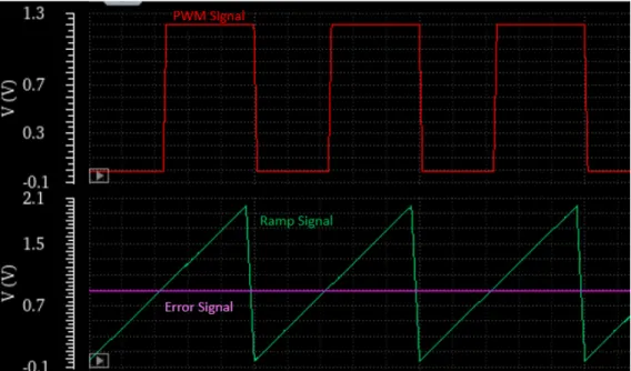
The reference voltage is connected to one of the inputs of the error amplifier, while the input of the other is connected to the feedback voltage of the buck converter's output. The following images illustrate the symbol of the generated ramp generator and its output waveform.
Introduction
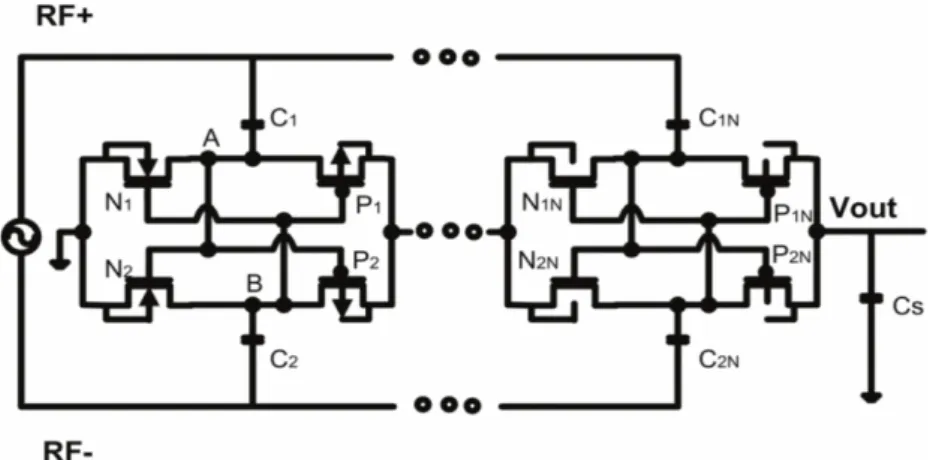
Diffrential Drive Rectifier
The output of the rectifier is connected to a smoothing capacitor to reduce the ripples of the output voltage. A load resistor is connected to the output of the rectifier to analyze the performance of the rectifier. To further study the efficiency of the proposed rectifier, a 2-step differential drive rectifier was built and simulated under the same condition to compare the performance with the single-step rectifier.
The circuit parameters used in a 2-stage rectifier are the same as in a single-stage rectifier. Then a load resistance test and the power generated by varying the load resistance from 625 to 1M will be done to determine the maximum power output that the two rectifiers can achieve. According to the obtained results, the single-stage rectifier has slightly higher output current and voltage in different resistive load ranges.
The peak output current, IL and peak output voltage, VOUT were recorded at a resistive load of 1 kΩ and 10 MΩ, respectively, for both rectifiers. A single-stage rectifier has a higher output power compared to a two-stage rectifier.
Buck Converter Simulation Results
If there is any difference between the 2 voltages, the error amplifier will produce an error signal. The generated error signal and the ramp voltage will then be compared by the comparator ("Incomparator" in Figure 4.11 above). If the error signal is higher than the ramp signal, the output of the comparator will be low.
Otherwise, when the error signal is lower than the ramp signal, the comparator will output a high signal to adjust the shift cycle as shown in the figure below. The reason the system takes 450 μs to reach its steady state may be due to the large size of the capacitor as the time to charge it increases. Since the rectifier also took about 13.7 μs to reach its steady state, the buck converter will take more time to stabilize the output voltage.
The proposed buck converter can step down the voltage of 6.75 V rectified by the rectifier to 3.3 V smoothly with an efficiency of 80.67. The proposed buck converter can step down the 6.75V generated from the rectifier to a stable 3.3V voltage with an efficiency of 80.67 which meets the specifications required initially.
Summary
Conclusion
Future Work
An ultra-low power CMOS image sensor with on-chip energy harvesting and power management capability. Panatik et al., "Energy harvesting in wireless sensor networks: A survey IEEE 3rd International Symposium on Telecommunication Technologies (ISTT), 2016, pp. Lucyszyn, "Ambient RF Energy Harvesting in Urban and Semi-Urban Environments," in IEEE Transactions on Microwave Theory and Techniques, vol.
Energy Harvesting Resources, Storage Devices, and System Topologies for Environmental Wireless Sensor Networks: A Review, ''Sensors, Vol. 34;Energy Harvesting From Human and Machine Motion for Wireless Electronic Devices," in Proceedings of the IEEE, vol. He, "Harvesting vibration energy in automobiles to power wireless sensors IEEE International Conference on Information and Automation, 2012, pp.
Roy et al., “A 6.45 microwatt self-powered SoC with integrated power management and ULP asymmetric radios for portable biomedical systems,” in IEEE Transactions on Biomedical Circuits and. Zhu, “Power Management Circuit for Wireless Sensor Nodes Powered by Energy Harvesting: On the Synergy of Harvester and Load,” in IEEE Transactions on Power Electronics, vol.