90 IEEE ELECTRON DEVICE LETTERS, VOL. 32, NO. 1, JANUARY 2011
High-Mobility Pentacene-Based Thin-Film
Transistors With a Solution-Processed
Barium Titanate Insulator
Chia-Yu Wei, Shu-Hao Kuo, Yu-Ming Hung, Wen-Chieh Huang,
Feri Adriyanto, and Yeong-Her Wang,
Member, IEEE
Abstract—Pentacene-based organic thin-film transistors (OTFTs) with solution-processed barium titanate(Ba1.2Ti0.8O3)
as a gate insulator are demonstrated. The electrical properties of pentacene-based TFTs show a high field-effect mobility of 8.85 cm2
·V− 1
·s−1, a low threshold voltage of−1.89 V, and a
low subthreshold slope swing of 310 mV/decade. The chemical composition and binding energy of solution-processed barium titanate thin films are analyzed through X-ray photoelectron spectroscopy. The matching surface energy on the surface of the barium titanate thin film is 43.12 mJ·m−
2
, which leads to Stranski–Krastanov mode growth, and thus, high mobility is exhibited in pentacene-based TFTs.
Index Terms—Barium titanate, high field-effect mobility, high permittivity, organic thin-film transistor (OTFT), solution process.
I. INTRODUCTION
R
ECENT years have seen increased attention paid to or-ganic thin-film transistors (OTFTs) because of their ap-plicability in flexible displays, large-area chemical sensors for artificial skin applications, and radio-frequency power trans-mission devices. To acquire better performance and more rapid carrier transport properties, gate dielectrics have become a prominent factor in improving gate capacitance, interfacial matching, and the orientation of semiconductor layers evapo-rated on dielectrics. Pentacene-based TFTs, with a high mobil-ity of 6.3 cm2·V−1
·s−1
achieved by using plasma treatment on sol-gel silica to improve the interface between the semicon-ductor and dielectric layers, have been reported [1]. Several inorganic metal oxide materials, such as magnesium oxide, titanium dioxide, and barium titanate [2]–[5], have been used as high-permittivity materials in integrated circuit fabrications and experimental research. Barium titanate, an oxide with a perovskite structure that could be used as ferroelectric materials
Manuscript received July 20, 2010; revised September 24, 2010; accepted September 25, 2010. Date of publication November 11, 2010; date of current version December 27, 2010. This work was supported in part by the Na-tional Science Council of Taiwan under Contracts NSC98-2627-E-006-003 and NSC98-2221-E-006-213-MY3. The review of this letter was arranged by Editor C.-P. Chang.
C.-Y. Wei is with the Institute of Electro-Optical Science and Engineering, National Cheng-Kung University, Tainan 701, Taiwan.
S.-H. Kuo, Y.-M. Hung, W.-C. Huang, and F. Adriyanto are with the Institute of Microelectronics, Department of Electrical Engineering, National Cheng-Kung University, Tainan 701, Taiwan.
Y.-H. Wang is with the Institute of Microelectronics, Department of Electri-cal Engineering, National Cheng-Kung University, Tainan 701, Taiwan, and also with the National Applied Research Laboratories, Taipei 106, Taiwan (e-mail: [email protected]).
Color versions of one or more of the figures in this letter are available online at http://ieeexplore.ieee.org.
Digital Object Identifier 10.1109/LED.2010.2084559
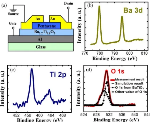
Fig. 1. (a) Cross-sectional diagram of a pentacene-based TFT with 250-nm barium titanate. XPS core level spectra of (b) Ba 3d, (c) Ti 2p, and (d) O 1s emissions from the solution-processed barium titanate thin film.
under Curie temperatures, exhibits a wide bandgap of 3.2 eV, indicating promising insulating property [6]. However, most high-permittivity inorganic metal oxide films should be de-posited under vacuum sputtering or electron-beam evaporating systems. For simpler processing and higher permittivity, barium titanate combined with solution-processed property was devel-oped, exhibiting high capacitance suitable for gate insulators. Solution-processed barium titanate thin films are demonstrated by spin coating under a low-cost deposition system. The cor-responding physical and electrical properties of barium titanate as the gate insulator of OTFTs are also investigated.
II. DEVICESTRUCTURE ANDFABRICATION
A cross-sectional diagram of the top contact pentacene-based TFT fabricated is shown in Fig. 1(a). Prior to the deposition of the common gate onto a Corning glass Eagle2000
substrate, the glass was cleaned with acetone, ethanol, and deionized water. An 80-nm-thick aluminum (Al) was deposited via a radio-frequency magnetron sputtering system with a “T”-shaped shadow mask as the gate electrode. The barium titanate solu-tion was produced by two steps. First, titanium isopropoxide (0.76 mL) was mixed with acetylacetone (0.51 mL) and then dissolved in 2-methoxythanol (3 mL), yielding the titanium-based solution. Second, to acquire the barium cations, barium acetate (638.5 mg) was added to glacial acetic acid (3 mL)
WEIet al.: HIGH-MOBILITY PENTACENE-BASED THIN-FILM TRANSISTORS 91
and heated on a 120 ◦C hot plate under stirring until the
barium acetate powder was completely dissolved. The barium cation solution was subsequently titrated into the titanium-based solution, and the barium titanate solution 0.5 M was prepared by adding 2-methoxythanol (2.73 mL). The barium titanate solution was spin-coated onto the Al/glass substrate several times to produce the desired transparent film thickness, as determined by an Alpha-step profiler. Each layer was baked on a hot plate at 180◦C for 10 min under ambient air conditions
in order to fulfill the future flexible electronics application. The pentacene film (65 nm) was thermally evaporated on the barium titanate insulator with a 0.847-nm rms surface roughness at a deposition rate of 0.08–0.15 nm/s. Finally, gold (Au) electrode patterns were defined through shadow masks and deposited by a radio-frequency magnetron sputtering system as both the source and drain. The corresponding channel length and width were 150 and 1500µm, respectively.
All measurements were obtained under atmospheric condi-tions at room temperature. The chemical composition and bind-ing energy of the barium titanate thin film were measured by X-ray photoelectron spectroscopy (XPS). The electrical strength of the barium titanate thin film and the electrical characteristics of the transistors were analyzed with a semicon-ductor parameter analyzer (HP 4156B). A FACE contact-angle meter (Kyowa Kaimenkagaku Co.) was used to measure the surface energy of the barium titanate thin film. Atomic force microscope (AFM) images were measured through the contact mode of a scanning probe microscope.
III. IMPLEMENTATION ANDPERFORMANCE
The chemical composition of the barium titanate thin film was analyzed by XPS. Fig. 1(b)–(d) shows the Ba 3d, Ti 2p, and O 1s emission spectra from the spin-coated barium titanate thin film. The XPS spectra of barium [Fig. 1(a)] show the doublet feature (779.6 and 795 eV). This phenomenon may be due to the splitting of the Ba 3d 5/2 and 3d 3/2 spin states. Fig. 1(c) shows the titanium 2p 3/2 and 2p 1/2 peaks of 457.4 and 463.4 eV, respectively. Focusing on the titanium 2p 3/2 peak, according to Mukhopadhyay and Chen (458.8 eV for sol-gel barium titanate thin films) and Nasser (455.5 eV for Ti2O3) [7], [8], the observed downshifting in the energy values of 1.4 eV may be due to the bonding of titanium with oxygen. Likewise, the titanium 2p 1/2 peak also shifted by 1.2 eV com-pared with the result of Mukhopadhyay and Chen (464.6 eV for sol-gel barium titanate thin films). An O 1s peak of 531.2 eV is shown in Fig. 1(d). The theoretical value of the O 1s peak from sol-gel barium titanate thin films was 530.25 eV, and a higher energy shift could have resulted from 531.7 eV of residual carbon contamination [9]. A good agreement between the simulated results composed of two different O 1s states and the measurement data was observed. Using the individual peak areas and sensitivity factors from XPS quantitative analysis data, the atomic percentages of barium, titanium, and oxygen were obtained (23.6%, 16.8%, and 59.7%, respectively). To sum up, the stoichiometric proportion of this solution-processed barium titanate thin film could be evaluated as Ba1.2Ti0.8O3.
The leakage current and permittivity of the barium titanate insulator were 4.78×10⁻⁸
A·cm−2
at ±1 MV·cm−1 and 15.57 which were measured through Al/barium titanate/Au
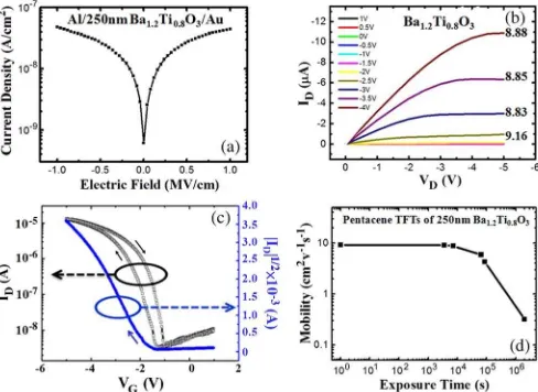
Fig. 2. (a) Leakage current density versus applied electric field(J−E)for the
metal/insulator/metal(Al/Ba1.2Ti0.8O3/Au)structure. (b) Current–voltage
characteristic curves of pentacene-based OTFTs with 250-nm barium titanate and (c) the transfer curves are also shown. (d) The plot of saturation field-effect mobilities as a function of exposure time under ambient conditions.
structures as shown in Fig. 2(a), respectively. In addition, Fig. 2(b) and (c) shows the output and transfer characteristics of pentacene-based OTFTs with a 250-nm barium titanate, which were measured at ambient atmosphere conditions immediately after fabrication at low gate–source voltages(VG), from 1 to
−5 V. Focusing on the barium titanate TFTs, a saturation drain current (ID)of 6.32 µA was obtained at aVG of−3.5 V. An on/off current ratio of about 3.77×10³
, threshold voltage(Vth) of−1.89 V, subthreshold slope swing (SS) of 310 mV/decade, and trap state density of 1.34×1011 cm−2
were calculated through the “OFF-to-ON state” transfer curve. The saturation field-effect mobility of 8.85 cm2
·V−1
·s−1
at aVGof−3.5 V could be calculated at a capacitance density of 55.12 nF·cm−2
. The different saturation field-effect mobilities corresponding to different gate biases are shown in Fig. 2(b). The hysteresis effect caused by ferroelectric properties shown in transfer curve might partially cause the instability of transistor performances but plays a key role to determine the memory window of fer-roelectric memory devices [10]. Fig. 2(d) shows the saturation field-effect mobilities plotted as a function of the exposure time under ambient conditions. After 106s, the saturation field-effect mobility decayed by about two orders to 0.32 cm2
·V−1
·s−1 because of moisture and oxidation. Nevertheless, this value can still be competitive with 0.34 cm2
·V−1
·s−1
obtained for 16% PEGPA-BT: PVP solution-processed gate insulators and 0.54 cm2
·V−1
·s−1
obtained for 11% PVP/BST nanocompos-ite dielectrics [4], [5], measured immediately after fabrication. Similar structure for the pentacene-based transistor with a 650-nm-thick barium titanate insulator was also fabricated. The corresponding field-effect mobility, Vth, and SS were 8.09 cm2
·V−1
·s−1
, −1.56 V, and 763 mV/decade, respec-tively. These data are all better than those of previously reported hafnium oxide insulator [11].
The contact angle data measured on the surface of bare barium titanate were 29.5◦ and 53.0◦ with ethylene glycol
and methylene iodide, respectively. Based on previous report [11], the surface energy of barium titanate was calculated to be 43.12 mJ·m−2
92 IEEE ELECTRON DEVICE LETTERS, VOL. 32, NO. 1, JANUARY 2011
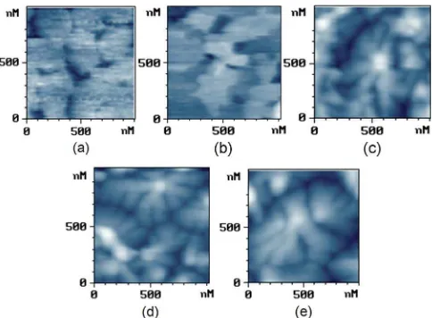
Fig. 3. AFM images(1 µm×1 µm)of (a) 2-nm, (b) 5-nm, (c) 10-nm,
(d) 35-nm, and (e) 65-nm pentacene films deposited on barium titanate. The large grain of 1.35µm is also seen in (e).
by expanding one lattice parameter in the crystal by incre-mental amounts, thus creating an internal surface, and by calculating the system energy at each increment. Therefore, the (001) surface energy of orthorhombic phase pentacene was 38 mJ·m−2
. Nevertheless, according to Yoshida et al. [13], the surface energy of different interfaces between dielectric layers and pentacene determined through experiments verified that the appropriate value is ranging from 42 to 48 mJ·m−2 for a 50-nm-thick pentacene. The calculated surface energy of the interface between 65-nm pentacene and barium titanate is consistent with the definition given by Yoshidaet al.Compared with the reported data using different substrates [11], [14], the higher mobility could be attributed to the appropriate surface energy between barium titanate and pentacene.
The interplanar spacing of pentacene layer is 1.54 nm which could be considered as the monolayer (ML) thickness of pen-tacene on barium titanate. To investigate the growth mode of pentacene on barium titanate, different thicknesses of 1, 3, 6, 23, and 42 ML are considered in Fig. 3(a)–(e). The AFM im-ages of 1 and 3 ML show the pentacene atoms diffusing to form a 2-D layer. The atoms bonded more densely to the substrate than to the other molecules. This is called the “layer mode.” The layer mode was also verified by the free nuclear density per micrometer square from the surface energy of 42–48 mJ·
m−2
[13]. After 6 ML, the grains turn out a layer mode structure. A herringbone island structure was observed when the interaction of pentacene molecules was stronger than that of the substrate. This growth mode of pentacene on barium titanate was found to be the Stranski–Krastanov (S-K) mode (layer-plus-island mode) [15]. The better transport properties from the S-K mode could be supported by a larger intermolecular coupling energy of 11.4 meV than that of Chenget al. [16]. Therefore, this phenomenon of the S-K mode results in signifi-cant enhancements of mobility, as reported by Qiet al.[17].
IV. CONCLUSION
In summary, high-mobility pentacene-based OTFTs with solution-processed barium titanate insulators have been demon-strated. The physical and chemical properties of solution-processed barium titanate thin film and performances of
pentacene-based TFTs have also been investigated. Solution-processed barium titanate oxide not only provides a high di-electric constant(κ=15.57)but also has good leakage current density (J =4.78×10⁻⁸
A·cm−2
) under ±1 MV·cm−1 . Moreover, the surface energy(γs) of the barium titanate thin film is 43.12 mJ·m−2
which is comparable to those with additional surface treatments. The matching surface energy on the barium titanate thin film leads to S-K mode growth. As such, a high field-effect mobility of 8.85 cm2
·V−1
·s−1 , a low threshold voltage of−1.89 V, and a low SS of 310 mV/decade can be yielded.
REFERENCES
[1] H. S. Tan, N. Mathews, T. Cahyadi, F. R. Zhu, and S. G. Mhaisalkar, “The effect of dielectric constant on device mobilities of high-performance, flexible organic field effect transistors,”Appl. Phys. Lett., vol. 94, no. 26, pp. 263 303-1–263 303-3, Jul. 2009.
[2] S. S. Cheng, C. Y. Yang, C. W. Ou, Y. C. Chuang, M. C. Wu, and C. W. Chu, “Pentacene thin-film transistor with PVP-capped high-kMgO dielectric grown by reactive evaporation,”Electrochem. Solid-State Lett., vol. 11, no. 5, pp. H118–H120, Feb. 2008.
[3] F. C. Chen, C. W. Chu, J. He, Y. Yang, and J.-L. Lin, “Organic thin-film transistors with nanocomposite dielectric gate insulator,”Appl. Phys. Lett., vol. 85, no. 15, pp. 3295–3297, Oct. 2004.
[4] P. Kim, X. H. Zhang, B. Domercq, S. C. Jones, P. J. Hotchkiss, S. R. Marder, B. Kippelen, and J. W. Perry, “Solution-processable high-permittivity nanocomposite gate insulators for organic field-effect transis-tors,”Appl. Phys. Lett., vol. 93, no. 1, pp. 013 302-1–013 302-3, Jul. 2008. [5] Y. Jang, W. H. Lee, Y. D. Park, D. Kwak, J. H. Cho, and K. Cho, “High field-effect mobility pentacene thin-film transistors with nanopar-ticle polymer composite/polymer bilayer insulators,”Appl. Phys. Lett., vol. 94, no. 18, pp. 183 301-1–183 301-3, May 2009.
[6] C. Hagendorf, K.-M. Schindler, T. Doege, and H. Neddermeyer, “A scan-ning tunneling microscopy, X-ray photoelectron spectroscopy and low energy electron diffraction investigation of the BaTiO3(111) surface,”
Surf. Sci., vol. 436, no. 1–3, pp. 121–130, Aug. 1999.
[7] S. M. Mukhopadhyay and T. C. S. Chen, “Surface chemical states of barium titanate: Influence of sample processing,”J. Mater. Res., vol. 10, no. 6, pp. 1502–1507, Jun. 1995.
[8] S. A. Nasser, “X-ray photoelectron spectroscopy study on the composition and structure of BaTiO3thin films deposited on silicon,”Appl. Surf. Sci., vol. 157, no. 1/2, pp. 14–22, Mar. 2000.
[9] B. Demri, M. Hage-Ali, M. Moritz, J. L. Kahn, and D. Muster, “X-ray photoemission study of the calcium/titanium dioxide interface,”Appl. Surf. Sci., vol. 108, no. 2, pp. 245–249, Feb. 1997.
[10] K. H. Lee, G. Lee, K. Lee, M. S. Oh, and S. Im, “Flexible low voltage non-volatile memory transistors with pentacene channel and ferroelectric poly-mer,”Appl. Phys. Lett., vol. 94, no. 9, pp. 093 304-1–093 304-3, Mar. 2009. [11] C.-Y. Wei, F. Adriyanto, Y.-J. Lin, Y.-C. Li, T.-J. Huang, D.-W. Chou, and Y.-H. Wang, “Pentacene-based thin-film transistors with a solution-process hafnium oxide insulator,”IEEE Electron Device Lett., vol. 30, no. 10, pp. 1039–1041, Oct. 2009.
[12] L. F. Drummy and D. C. Martin, “Thickness-driven orthorhombic to tri-clinic phase transformation in pentacene thin films,”Adv. Mater., vol. 17, no. 7, pp. 903–907, Apr. 2005.
[13] M. Yoshida, S. Uemura, T. Kodzasa, T. Kamata, M. Matsuzawa, and T. Kawai, “Surface potential control of an insulator layer for the high per-formance organic FET,”Synthetic Met., vol. 137, pp. 967–968, Apr. 2003. [14] W. Y. Chou, C. W. Kuo, H. L. Cheng, Y. R. Chen, F. C. Tang, F. Y. Yang, D. Y. Shu, and C. C. Liao, “Effect of surface free energy in gate dielectric in pentacene thin-film transistors,” Appl. Phys. Lett., vol. 89, no. 11, pp. 112 126-1–112 126-3, Sep. 2006.
[15] R. Ruiz, D. Choudhary, B. Nickel, T. Toccoli, K.-C. Chang, A. C. Mayer, P. Clancy, J. M. Blakely, R. L. Headrick, S. Iannotta, and G. G. Malliaras, “Pentacene thin film growth,”Chem. Mater., vol. 16, no. 23, pp. 4497– 4508, Nov. 2004.
[16] H.-L. Cheng, W.-Y. Chou, C.-W. Kuo, Y.-W. Wang, Y.-S. Mai, F.-C. Tang, and S.-W. Chu, “Influence of electric field on microstructures of pentacene thin films in field-effect transistors,”Adv. Funct. Mater., vol. 18, no. 2, pp. 285–293, Jan. 2008.