ISSN: 1693-6930
Accredited by DGHE (DIKTI), Decree No: 51/Dikti/Kep/2010 477
Numerical Simulation of Tunneling Current in an
Anisotropic Metal-Oxide-Semiconductor Capacitor
Fatimah A. Noor*, Ferry Iskandar, Mikrajuddin Abdullah, Khairurrijal¥
Physics of Electronic Materials Research Division, Faculty of Mathematics and Natural Sciences, Institut Teknologi Bandung
Jalan Ganesa 10, Bandung 40132, Indonesia, telp/fax: +622 2500834/+622 2506452 e-mail: [email protected]*, [email protected]¥
Abstrak
Pada makalah ini telah dikembangkan sebuah model arus terobosan yang melalui kapasitor MOS dielektrik ganda dengan melibatkan massa anisotropik. Transmittansi dihitung secara numerik dengan menggunakan metode transfer matriks dan menyertakan efek kopling antara energi longitudinal dan kinetik yang diwakili oleh kecepatan fasa elektron di gerbang. Transmittansi yang diperoleh kemudian digunakan untuk menghitung arus terobosan di dalam kapasitor MOS TiN/HfSiOxN/SiO2/p-Si. Hasil
perhitungan menunjukkan bahwa seiring bertambahnya kecepatan elektron, transmittansi menurun dan arus terobosan berkurang. Arus terobosan menurun seiring dengan bertambahnya ketebalan oksida setara untuk lapisan HfSiOxN. Saat arah elektron datang menembus penghalang tegak lurus antarmuka
lapisan, proses terobosan elektron menjadi lebih mudah. Diperoleh pula bahwa arus terobosan tidak bergantung pada orientasi substrat. Lebih lanjut, model yang diajukan dapat digunakan dalam mendesain divais MOS berkecepatan tinggi dengan arus terobosan yang rendah.
Kata kunci: arus terobosan, kecepatan gerbang, massa anisotropik, material berkonstanta dielektrik tinggi, metode transfer matriks.
Abstract
In this paper, we have developed a model of the tunneling current through a high- dielectric stack in MOS capacitors with anisotropic masses. The transmittance was numerically calculated by employing a transfer matrix method and including longitudinal-transverse kinetic energy coupling which is represented by an electron phase velocity in the gate. The transmittance was then applied to calculate tunneling currents in TiN/HfSiOxN/SiO2/p-Si MOS capacitors. The calculated results show that as the gate
electron velocity increases, the transmittance decreases and therefore the tunneling current reduces. The tunneling current becomes lower as the equivalent oxide thickness (EOT) of HfSiOxN layer increases.
When the incident electron passed through the barriers in the normal incident to the interface, the electron tunneling process becomes easier. It was also shown that the tunneling current was independent of the substrate orientation. Moreover, the model could be used in designing high speed MOS devices with low tunneling currents.
Keywords: anisotropic mass, gate velocity, high-κ dielectric stack, transfer matrix method, tunneling current
1. Introduction
It is known that silicon-based metal-oxide-semiconductor field-effect transistors (MOSFETs) are aggressively scaled down to the sub-micrometer regime and below for emerging applications required higher speed, higher density and lower voltage operation [1-2]. In order to fulfill these aims, it is required a thinner SiO2 gate oxide. However, a vast tunneling
current arises and power dissipation becomes significantly high when the gate oxide thickness is less than 1.5 nm [3]. In order to solve these problems, it is needed a high- κ dielectric with equivalent electrical oxide thickness but higher physical thicknesses to replace SiO2 such as
Ta2O5, Al2O3, ZrO2, HfO2, La2O3, TiO2, Lu2O3, Y2O3, SrTiO3 [4-7]. Since having good dielectric
properties and good thermal stability on silicon substrates, Hf-based silicates are the promising candidate to replace SiO2 compared to other high- κ materials [8-10]. The gate oxides
anticipated to substitute SiO2 are a stack of an ultrathin SiO2 and a high- κ layer, which is known
Several methods have been utilized to compute a transmittance and tunneling current in high- κ gate stack based MOS capacitors [11-17]. However, they did not consider the coupling effects between longitudinal and transverse motions and anisotropic mass in the MOS capacitors. On the other hand, we have very recently developed an analytical model of tunneling in a TiN/HfSiOxN/SiO2/p-Si MOS capacitor by using Airy wave function approach
which is including the coupling between longitudinal and transverse motions that is represented by an electron velocity in the metal gate [18]. In addition, it has been experimentally revealed that a high speed MOSFET was realized by injecting high velocity electrons [19].
In this paper, we report a numerical model of transmittance and tunneling current through a high-κ dielectric stack by including a longitudinal-transverse kinetic energy coupling, which is represented by a gate electron-phase velocity and an anisotropic electron mass by using the transfer matrix method. The transfer matrix method has been extensively utilized to study quantum-mechanical tunneling through potential barriers because this method is known to be more accurate than the other method [20]. This model is then applied to calculate the transmittance and tunneling current in TiN/HfSiOxN/SiO2/p-Si MOS capacitors. The
transmittance and tunneling current as a function of the electron phase velocity in metal gate is studied. In addition, the effect of equivalent oxide thickness (EOT), the incident angle of electron, and the substrate orientation on the transmittance and tunneling current are investigated also.
2. Theoretical Model
We use the model on Ref. [3] in computing tunneling currents in TiN/HfSiOxN/SiO2/p-Si
MOS capacitors. The description of an electron in an anisotropic material under the parabolic-band effective mass approximation is used as a first step in the model which is described as [21].
( )
r
p
( ) ( )
r
( )
r
p
T
Λ
=
Λ
+
V
z
E
m
02
1
α
, (1)
where
p
is the momentum vector, m0 is the free-electron mass,α
(
r
)
m
0is the inverse effective-mass tensor, V(z) is the potential energy which is only dependent on the z-direction, E andΛ
( )
r
are the electron total energy and wavefunction, respectively. One dimensional Schrödinger-like equation in the z-direction is obtained by employing the separation method.Since the total energy E is composed of the longitudinal (the z-direction) and the transverse (the x-y plane) energies is written as
E
=
E
z+
E
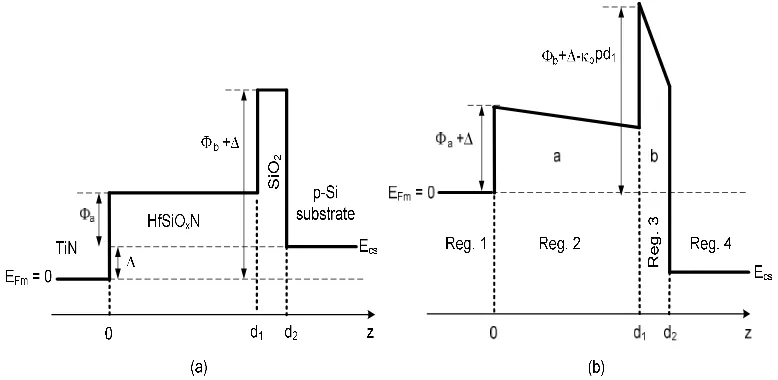
xy , the one dimensional Schrödinger-like equation has a coupling term between longitudinal and transverse kinetic energies of electron motion in the anisotropic heterostructure, which is represented by a phase velocity in the TiN gate. Figure 1 gives the potential profile of the conduction band energy in which the conduction band differences between HfSiOxN and Si, SiO2 and Si, and TiN and Si are Φa, Φb, and ∆,respectively, and d1 and (d2-d1) are the thicknesses of HfSiOxN and SiO2, respectively.
The potential profile in Figure 1 is mathematically expressed as
(
)
≥
∆
−
−
<
≤
−
−
+
∆
+
Φ
<
≤
−
∆
+
Φ
<
=
,
)
(
)
(
0
)
(
0
0
)
(
2 2 1 1 b 1 ad
z
eV
d
z
d
pz
pd
d
z
pz
z
z
V
ox a b a bκ
κ
κ
κ
(2) where 1 1 2)
(
d
d
d
eV
p
b a oxκ
κ
−
+
=
, e is the electronic charge, Vox is the oxide voltage which isthe voltage across the barrier, d1 and (d2-d1) are the thicknesses of HfSiOxN and SiO2,
respectively, and κa and κb are the dielectric constants of HfSiOxN and SiO2, respectively.
The potential profile of regions 2 and 3 in Figure 1 under the transfer matrix method (TMM) are divided into N segments of rectangular form as described in Figure 2.
Figure 2. The potential profile separated into N segments
Therefore, for the nth segment, the wave function can be approximated as [20]
( )
( )
(
)
{
} (
)
( )
(
)
{
} (
)
( )
(
)
{
} (
)
(
)
{
} (
)
≥
−
<
≤
−
−
+
<
≤
−
−
+
<
−
−
+
=
Θ
,
exp
exp
exp
exp
exp
0
exp
exp
exp
0
exp
exp
exp
2 4 2 1 3 1 2 1 1 1 1d
z
z
i
z
i
A
d
z
d
z
i
z
B
z
A
d
z
z
i
z
B
z
A
z
z
i
z
i
B
z
i
z
N N n n n n n n n n nγ
δ
γ
δ
δ
γ
δ
δ
γ
δ
δ
(3)1 , 2 1 , 0 1
1
2
zz zE
m
α
δ
h
=
, 2 1 1 , } , {, ,1
, 1 , 0 2 2
1
2
2
−
−
−
=
∑
∈xy z
j i ij n ij ij j i n s n
E
m
k
k
V
m
β
β
β
δ
h
h
and 4 , 2 } , {, ,1
4 , 1 , 0 2 1 , 0
1
1
2
)
(
2
zz y x j i ij ij ij j i N z Nm
k
k
z
V
E
m
α
β
β
β
δ
h
h
−
−
−
=
∑
∈,
respectively, mn is theelectron effective mass, and Vn and VN are the constant potential in the nth for 1<n<N and N th
segments. The term of z,1
y} {x, j i, ij,1 n ij, ij,1 0 j i 2 n
E
β
β
1
β
2m
k
k
V
−
−
−
∑
∈h
is known as the effective
potential.
By applying the boundary conditions [22] of successive segments, it is easily obtained the total transfer matrix for N segments as follows:
=
−0
...
1
1 34 23 12 1 N N NA
M
M
M
M
B
,
(4)where Mnn+1 is a matrix relating An and Bn with An+1 and Bn+1.
Articulating M12M23M34…..MN-1N as
Γ
Γ
Γ
Γ
=
Γ
22 21 12 11, the term f becomes
11
1
Γ
=
=
A
Nf
.
(5)The transmittance T(Ez) is found as
( )
* 1 , 1 4 ,. f
f
E
T
zz zz Nz
δ
α
α
δ
=
.
(6)The electron transmittance is then employed to calculate the tunneling current which is given by [18]
[
]
(
)
(
)
[
]
zox z F z F z
l vl dl
z
dE
kT
eV
E
E
kT
E
E
kT
E
T
m
n
e
J
∑
∫
∞
−
∆
+
−
+
−
+
×
=
0 3 2)
(
exp
1
)
(
exp
1
ln
)
(
2
λπ
h
,
(7)where nv and md are the number of valleys and the density of states mass, respectively, T(Ez) is
the electron transmittance, k is the Boltzmann constant, and T is the temperature. The tunneling current in Equation (7) is easily computed by using the Gauss–Laguerre Quadrature method [23].
3. Results and Discussion
In present model, the quantization effect of the p-type Si accumulation layer is negligible to avoid requiring more numerical treatment. In order to calculate the transmittance and tunneling current, it was used the following parameters: Φa= 1.52 eV, Φb= 3.34 eV, ∆= 0.53 eV,
d1= 0.5 nm, κa= 13.5, κb= 3.9 [18]. The electron effective mass in the HfSiOxN and TiN metal
electron effective mass in SiO2 is also isotropic and assumed to be m0 for the thickness of 0.5
nm as extrapolated from Ref. [12]. Since there are six equivalent valleys in the conduction band of Si which are divided into three groups of valleys, the tensor elements of Si(100), Si(110), and Si(111) are given in Tables 1, 2, and 3, respectively [25-27].
Table 1. Tensor elements αij of Si(100)
Valley Si(100)
V1
1.02 0 0
0 5.26 0
0 0 5.26
V2
5.26 0 0
0 1.02 0
0 0 5.26
V3
5.26 0 0
0 5.26 0
0 0 1.02
Table 2. Tensor elements αij of Si(110)
Valley Si(110)
V1
5.26 0 0
0 3.14 2.12 0 2.12 3.14
V2
5.26 0 0
0 3.14 -2.12 0 -2.12 3.14
V3
1.09 0 0
0 5.26 0
0 0 5.26
Table 3. Tensor elements αij of Si(111)
Valley Si(111)
V1
4.57 1.21 0.98
1.21 3.14 -1.70
0.98 -1.70 3.87
V2
4.57 -1.21 0.98
-1.21 3.14 1.70
0.98 1.70 3.87
V3
2.48 0 -1.97
0 5.26 0
-1.97 0 7.74
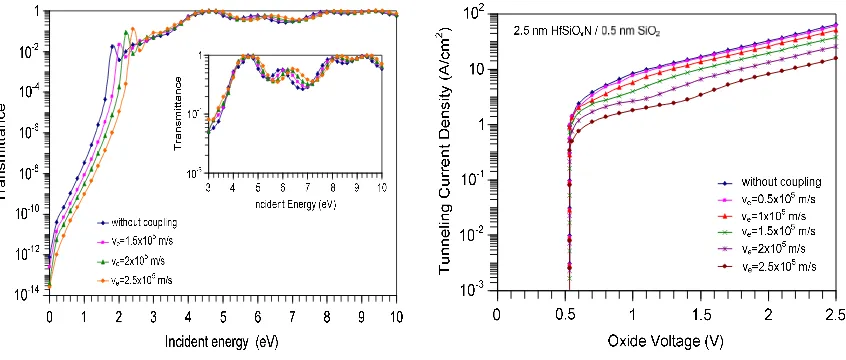
Figure 3 compares the transmittances of electrons in the valley 1 (V1) moving from the metal gate with phase velocities in the range of 1.5 – 2.5×10⁵ m/s and tunneling through a barrier composed of 2.5 nm-thick HfSiOxN and 0.5 nm-thick SiO2 layers for the oxide voltage of 1 V
with that without considering the coupling effect of the longitudinal and transversal kinetic energies.
Figure 3. Electron transmittance in the MOS capacitor calculated without and with
considering the coupling effect
Figure 4. Electron tunneling current density in the MOS capacitor calculated without the
It is seen that the transmittances increase as the incident electron energy increases. For incident electron energies higher than the barrier height, the transmittances show oscillatory behaviors as given in the inset. It is also shown that the transmittance calculated without the coupling effect is much higher than those obtained by including the gate electron phase velocities in the range of 1.5 to 2.5×10⁵ m/s. In addition, the increase of the gate electron velocity reduces the transmittance. This is because the gate electron velocity causes an effective potential barrier Veff(z) higher than the barrier V(z) as already explained in Refs. [3,
28-29].
Employing the same parameters as used in obtaining Figure 3, electron tunneling current density, which is contributed from each valley, was calculated. The tunneling current density as a function of oxide voltage is depicted in Figure 4. It is found that the tunneling current density increases with the oxide voltage. In addition, the electron tunneling process from the metal gate to the silicon substrate does not happen for the oxide voltages lower than 0.53 V as demonstrated in Figure 1 because electrons in the Fermi level of TiN metal gate can not occupy the forbidden states of p-Si substrate band gap [18]. The tunneling current density calculated without the coupling effect of longitudinal-transverse kinetic energy is the highest as compared to those obtained by including the coupling effect. It is also found that the increase of the gate electron velocity reduces the tunneling current density. This is because the barrier height V(z) in Equation (2) is enhanced by the increase of the gate electron phase velocity. The transmittance is, therefore, reduced. Moreover, the slopes of the curves in Figure 4 are almost identical. This finding means that the modification of potential barrier can be compensated for the electron effective mass of the tunneling barrier. This is an indication that the inclusion of the gate electron phase velocity in the present model could be used to explain the achievement of a high-speed source-heterojunction MOS transistor due to the injection of high velocity electrons as reported in Ref. [19].
Figure 5. The relation between the tunneling current and equivalent oxide thickness (EOT)
in the MOS capacitor TiN/HfSiOxN/SiO2/p-Si(100)
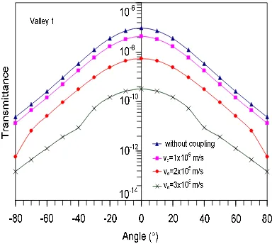
Figure 6. The electron transmittance versus the incident angle of electron
To verify the effects of longitudinal-transverse kinetic energy coupling and equivalent oxide thickness (EOT) to tunneling current, the calculated tunneling currents for a stack of 0.5 nm interfacial SiO2 and HfSiOxN with and without the coupling effect are demonstrated in Figure
5. It is found that the coupling effect can not be neglected in tunneling current in the MOS capacitor for thick HfSiOxN layer. Moreover, as the EOT (effective oxide thickness) of HfSiOxN
layer increases, the tunneling current becomes lower. It means that the usage of HfSiOxN as the
gate oxide can reduce the tunneling current as explained in Refs. [3] and [18].
longitudinal-transverse kinetic energy. In this problem, we use the coordinate system as shown in Figure 7. Noting that the total energy E is composed of Exy and Ez, where Exy and Ez are the
transverse and longitudinal energies, respectively, the total energy becomes
[
(
sin
cos
sin
sin
cos
cos
)
]
}
.
2
cos
1
2
2 2
2
2 2
} , { , 2 0
0 2
ϕ
θ
θ
α
ϕ
θ
θ
α
θ
α
β
k
k
k
m
v
m
E
zx yz
zz y
x j
i ij
e
+
+
+
=
∑
∈
h
h
.
(8)We calculate the direct transmittance with the angles of incident electron θ and ϕ. We fix ϕ to π/2 and change only θ for simplicity. From the figure, it is shown that the transmittance decreases as the gate electron phase velocity increases as also given in Figure 4. It is also shown that the transmittance gives the highest value at the incident angle of 0° (normal incident to the interface). It means that for the incident angle of 0°, the movement of electron becomes easier. These results are the same as those obtained with the analytical method given in Ref. [30].
Figure 7. The coordinate system used in this problem
Figure 8. The tunneling current in the TiN/HfSiOxN/SiO2/p-Si MOS capacitor for different
substrate orientations
Figure 8 demonstrates the effect of substrate orientation to the electron tunneling current. Here, it was used the electron incident angle of 0o and the gate electron velocity of 105 m/s. It is seen that the tunneling currents give the same result for the substrate orientations of Si(100), Si(110), and Si(111). It means that the tunneling current in the TiN/HfSiOxN/SiO2/p-Si
capacitor is not affected by the substrate orientation. The result is also consistent with that, which obtained analytically as given in Ref. [3].
4. Conclusion
We have studied numerically the electron tunneling current density TiN/HfSiOxN/SiO2
/p-Si MOS capacitor. The transmittance through the barrier is derived by including the effect of a longitudinal-transverse kinetic energy coupling represented by the gate electron phase velocity. It has been shown that the increase of the gate electron velocity enhances the barrier height, decreases the transmittance, and therefore reduces the tunneling current density. It has also been shown that the tunneling current becomes lower as the EOT increases. In addition, it was found that the tunneling process in TiN/HfSiOxN/SiO2/p-Si capacitor becomes easier when the
depend on the substrate orientation. Furthermore, the present results suggest that the MOS device could operate at a high speed with a low tunneling current when electrons from the gate could be injected with a high phase velocity.
Acknowledgment
This work was supported by a research grant from the Asahi Glass Foundation in the fiscal year of 2011
References
[1] Govoreanu B, Blomme P, Rosmeulen M, Houdt J V, Meyer K D. A Model for Tunneling Current in Multi-layer Tunnel Dielectrics. Solid-State Electronics. 2003; 47(6): 1045-1053
[2] Iwai H, Momose H S, Katsumata Y. Si-MOSFET Scaling Down to Deep-sub-0.1-micron Range and Future of Silicon LSI. International Symposium on VLSI Technology System and Applications. 1995; 31: 262-267
[3] Khairurrijal, Noor F A, Abdullah M, Sukirno, Miyazaki S. Theoretical Study on Leakage Current in MOS with High-K Dielectric Stack: Effects of In-plane-Longitudinal Kinetic Energy Coupling and Anisotropic Masses. Transactions of the Materials Research Society of Japan. 2009; 34(2): 291-295 [4] Wilk G D, Wallace R M, Anthony J M. High-k Gate Dielectrics: Current Status and Materials Properties
Considerations. Journal of Applied Physics. 2001; 89(10): 5243-5275
[5] Green M L, Gusev E P, Degraeve R, Garfunkel E. Ultrathin (<4 nm) SiO2 and Si-O-N Gate Dielectric Layers for Silicon Microelectronics: Understanding the Processing, Structure, and Physical and Electrical Limits. Journal of Applied Physics. 2001; 90(5): 2057-2121
[6] Copel M, Gribelyuk M, Gusev E. Structure and Stability of Ultrathin Zirconium Oxide Layers on Si(001). Applied Physics Letters. 2000; 76(4): 436-438
[7] Ferrari G, Watling J R, Roy S, Barker J R, Asenov A. Beyond SiO2 Technology: Simulation of the Impact of High-k Dielectrics on Mobility. Journal of Non-Crystalline Solids. 2007; 353(5-7): 630-634 [8] Chiu F –C. Interface characterization and carrier transportation in metal/HfO2/silicon structure. Journal
of Applied Physics. 2006; 100(11): 114102-1-114102-5
[9] Pei Y, Ohta A, Murakami H, Higashi S, Miyazaki S, Akasaka T, Nara Y. Analysis of Leakage Current through Ultrathin HfSiOxN/SiO2 Stack Gate Dielectric Capacitors with TiN/W/TiN Gate. International
Workshop on Dielectric Thin Films for Future ULSI Devices – Science Technology. Kanagawa. 2006; 107-108
[10] Chowdhury N A, Misra D. Charge Trapping at Deep States in Hf–Silicate Based High-k Gate Dielectrics. Journal of Electrochemical Society. 2007; 154(2): G30-G37
[11] Khairurrijal, Noor, F A, Sukirno. Electron Direct Tunneling Time in Heterostructures with Nanometer-thick Trapezoidal Barriers. Solid-State Electronics. 2005; 49(6): 923-927
[12] Khairurrijal, Mizubayashi W, Miyazaki S, Hirose M. Analytic Model of Direct Tunnel Current through Ultrathin Gate Oxides. Journal of Applied Physics. 2000; 87(6): 3000-1-3000-5
[13] Noor F A, Abdullah M, Sukirno, Khairurrijal. Comparison of Electron Direct Transmittance and Tunneling Time of Si(100)/HfO2/Si(100) and Si(110)/HfO2/Si(110) Structures with Ultra-thin Trapezoidal Barrier. Indonesian Journal of Physics. 2007; 18(2): 41-45
[14] Zhao Y, White M H. Modeling of Direct Tunneling Current through Interfacial Oxide and High-k Gate Stacks. Solid-State Electronics. 2004; 48(10-11): 1801-1807
[15] Wu H, Zhao Y, White M H. Quantum Mechanical Modeling of MOSFET Gate Leakage for High-k Gate Dielectrics. Solid-State Electronics. 2006; 50(6): 1164-1169
[16] Chen W B, Xu J P, Lai P T, Li Y P, Xu S G. Gate Leakage Properties of MOS Devices with Tri-Layer High-k Gate Dielectric. Microelectronics Reliability. 2007; 47(6): 937-943
[17] Kauerauf T, Govoreanu B, Degraeve R, Groeseneken G, Maes H. Scaling CMOS: Finding the Gate Stack with the Lowest Leakage Current. Solid-State Electronics. 2005; 49(5): 695-701
[18] Noor F A, Abdullah M, Sukirno, Khairurrijal, Ohta A, Miyazaki S. Electron and hole components of tunneling currents through an interfacial oxide-high-k gate stack in metal-oxide-semiconductor capacitors. Journal of Applied Physics. 2010; 108(9): 093711-1-093711-4
[19] Mizuno T, Sugiyama N, Tezuka T, Moriyama Y, Nakaharai S, Maeda T, Takagi S. High-Speed Source-Heterojunction-MOS-Transistor (SHOT) Utilizing High-Velocity Electron Injection. IEEE Transactions on Electron Devices. 2005; 52(12): 2690-2696
[20] Abdolkader T M, Hassan M M, Fikry W, Omar O A. Solution of Schrodinger equation in double-gate MOSFETs using transfer matrix method. Electronics Letters. 2004; 40(20): 1-2
[21] Kim K –Y, Lee B. Tunneling Time and the Post-Tunneling Position of an Electron through a Potential Barrier in an Anisotropic Semiconductor. Superlattices and Microstructure. 1998; 24(6): 389-391 [22] Kim K –Y, Lee B. Transmission Coefficient of an Electron through a Heterostructure Barrier Grown on
[23] De Vries P L. A First Course in Computational Physics, Second Edition. New York: Wiley. 1993 [24] Szczyrbowski J. A New Simple Method of Determining the Effective Mass of an Electron or the
Thickness of Thin Metal Films. Journal of Physics D: Applied Physics, 1986; 19(7): 1257-1263
[25] Yi K S, Quinn J J. Linear Response of a Surface Space-Charge Layers in Anisotropic Semiconductor. Physical Review B. 1983; 27(2): 1184-1990
[26] Yi K S, Quinn J J. Optical Absorpsion and Collective Modes of Surface Space-Charge Layers on (110) and (111) Silicon. 1983. Physical Review B, 27(4): 2396-2411
[27] Rahman A, Lundstrom M S, Ghosh A W. Generalized Effective-mass Approach for n-Type Metal-Oxide-Semiconductor Field-Effect Transistor on Arbitrarily Oriented Wafers. Journal of Applied Physics. 2005; 97(5): 053702-1053702-12
[28] Hasanah L, Abdullah M, Sukirno, Winata T, Khairurrijal. Model of a Tunneling Current in an Anisotropic Si/Si1−xGex/Si Heterostructure with a Nanometer-thick Barrier Including the Effect of
Parallel–Perpendicular Kinetic Energy Coupling. Semiconductor Science and Technology. 2008; 23(12): 125024-1-125024-6
[29] Noor F A, Abdullah M, Sukirno, Khairurrijal. Comparison of Electron Transmittances and Tunneling Currents in an Anisotropic TiNx/HfO2/SiO2/p-Si(100) Metal–Oxide–Semiconductor (MOS) Capacitor. 2010. Journal of Semiconductors. 31(12):124002-1-124002-5