ULTRA-THIN BODY SOI 22NM N-MOSFET (THE EFFECT TiN GATE THICKNESS)
NOR JANNATI BINTI ABD HALIM
A thesis submitted in partial fulfillment of the requirements for the award of the degree of Bachelor of Electronic Engineering (Computer Engineering)
Faculty of Electronic and Computer Engineering Universiti Teknikal Malaysia Melaka
v
vi
ACKNOWLEDGEMENT
Firstly, ‘In the name of Allah, most gracious, most merciful’. Alhamdulillah, I would like to extend my deep gratitude towards the almighty Allah S.W.T because of His mercy and kindness, I was able to complete my Final Year Project and thesis in a given time frame without having any difficult problems. I would like to express profound gratitude to my Final Year Project Supervisor, Pn. Niza Binti Md. Idris for her invaluable support, encouragement, supervision and useful knowledge throughout this duration of my project. And also like to thank my father, Abd. Halim Bin Ismail, my beloved mother, Sopiah Binti Taib, for their love and support me all time through my life, give me the spirit and pray for my success in carrying out the task. Thank you to my caring fiancée that always concern about me and give me motivation when I need them. Last but not least, thanks to my brother and little sister who always supports me. Thanks for their encouragement that they had given to me. Special thanks goes to Dr. Anis Suhaila Binti Mohd Zain for sharing their knowledge regarding “Silvaco software”. With their help, I able to finish my project on time. Nevertheless, my great appreciation dedicated to my friend Fidzrie Hafiz Bin Razali, Nor Idayu Binti Che Hussin and Rabiatul Adawieyah Binti Awang Ali, who had shared their opinion and knowledge directly or indirectly with this project. Finally, I am also thankful to my colleagues of Electronic and Computer Engineering and to all my friends in Universiti Teknikal Malaysia Melaka for their assistance and understanding.
Thank you so much
vii
ABSTRACT
viii
ABSTRAK
ix
TABLE OF CONTENT
CHAPTER TITLE PAGE
PROJECT TITLE
REPORT STATUS VERIFICATION FORM DECLARATION SUPERVISOR DECLARATION DEDICATION ACKNOWLEDGEMENT ABSTRACT ABSTRAK
TABLE OF CONTENTS LIST OF TABLE
LIST OF FIGURE
LIST OF ABBREVIATIONS LIST OF APPENDIX
i ii iii iv v vi vii viii ix xii xiii xvi xvii
1 INTRODUCTION
1.1 Introduction of Silicon On Insulator (SOI) 1.2 Objectives
1.3 Scope
x
2 LITERATURE REVIEW
2.1 Introduction
2.2 Bulk MOSFET/ Conventional MOSFET 2.3 Ultra-Thin Body Soi (UTB)
2.4 Fully Depletion 2.5 I-V Characteristic 2.6 Leakage Current 2.7 Drive Current 2.8 Sub-Treshold Slope 2.9 Threshold Voltage 2.10 Scaling MOSFET 2.11 Short Channel Effect
6 7 9 9 10 11 11 12 12 14 16
3 METHODOLOGY
3.1 Introduction 3.2Overall Flow Chart
3.3TCAD Process Structure Framework
3.3.1 Athena-Process Simulation Framework 3.3.2 Atlas-Process Simulation Framework 3.3.3 Deckbuild Process Structure Framework 3.422nm UTB SOI Design
3.5Process to Design Structure Device 3.5.1 Athena
3.5.2 Atlas
xi
4 RESULT AND DISCUSSION
4.1 Introduction
4.2 Device Description 4.3 Result after simulation
4.4Comparison of 5nm, 10nm, 15nm, 20nm, and 25nm Titanium Thickness for 22nm Gate Length
4.4.1 Drain Voltage 0.87V for 5nm titanium thickness 4.4.2 Drain Voltage 0.87V for 10nm titanium thickness 4.4.3 Drain Voltage 0.87V for 15nm titanium thickness 4.4.4 Drain Voltage 0.87V for 20nm titanium thickness 4.4.5 Drain Voltage 0.87V for 25nm titanium thickness 4.4.6 Drain Voltage 0.05V for 5nm titanium thickness 4.4.7 Drain Voltage 0.05V for 10nm titanium thickness 4.4.8 Drain Voltage 0.05V for 15nm titanium thickness 4.4.9 Drain Voltage 0.05V for 20nm titanium thickness 4.4.10 Drain Voltage 0.05V for 25nm titanium thickness 4.5 Summary of the result for comparisons 5nm,10nm,
15nm, 20nm, and 25nm titanium gate thickness for 22nm gate length
39 39 45 51 51 53 55 57 59 61 63 65 67 69 71
5 CONCLUSION AND RECOMMENDATIONS
5.1 Conclusion
5.2 Recommendations
xii
LIST OF TABLE
NO. TITLE PAGE
2.1 Parameter of High Standby Power Technology (2011) 15 4.1
4.3 4.4
Parameter scale of gate length, Lg = 22nm titanium Result for 0.87V voltage supply
Result for 0.05V voltage supply
xiii
LIST OF FIGURE
NO. TITLE PAGE
1.1 The physical structure of UTB SOI 2
2.1 2.2 2.3 2.4 2.5 2.6 2.7 2.8 2.9 2.10
N- channel Mosfet (NMOS) Structure The P MOSFET structure
The depletion type of n-channel MOSFET Ultra-Thin Body Soi Structure
Front-channel characteristics of a fully-depleted n-channel SOI MOSFET
I-V Characteristics of N-MOSFET
Common- source circuit driven by a constant current source used for the determination of the pinch-off and the slope factor as functions of VG
Graph threshold voltage for n- channel and p- channel MOSFET Scaling
Scaling of switches
6 7 8 9 10 11 12 13 14 15 3.1 3.2 3.3 3.4 3.5 3.6 3.7 3.8 3.9 3.10 3.11 3.12 3.13 3.14
Overall Flow Chart of this project View Grid Window
Selecting Display The material Silicon from TONYPLOT Process deposition oxide
Process deposition Silicon Process to grow gate oxide layer
Process to remove unwanted oxide layers Structure before process implant
Structure after process implant Process to remove all oxide layers Process to define EOT
Process to add the gate layer
Process to remove titanium to get the gate length Structure After Spacer Oxide Deposition.
xiv 3.15 3.16 3.17 3.18 3.19 3.20
Sidewall Spacer Oxide Formation after Dry Etching. Process Etch the oxide layer to deposit the aluminum layer Aluminum Deposition on the Half NMOS structure Etching Aluminum on the Half NMOS structure.
Complete to design the full structure 22nm body soi n-MOSFET
Full structure device with Contour Plot
33 34 35 36 37 37 4.1 4.2 4.3 4.4 4.5 4.6 4.7 4.8 4.9 4.10 4.11 4.12 4.13 4.14 4.15 4.16 4.17 4.18 4.19 4.20 4.21 4.22 4.23 4.24 4.25 4.26
UTB N-MOSFET design with 22nm gate length Contour structure after doping
UTB N-MOSFET design with mesh
UTB N-MOSFET design with 5nm titanium thickness UTB N-MOSFET design with 15nm titanium thickness UTB N-MOSFET design with 20nm titanium thickness UTB N-MOSFET design with 25nm titanium thickness Show the linear graph for high voltage
Show the log graph for high voltage Show the linear graph for low voltage Show the log graph for low voltage
Show the linear graph for overlay UTB high and UTB low Show the log graph for overlay UTB high and UTB low Show the linear graph high voltage
Show the log graph for high voltage Show the linear graph high voltage Show the log graph for high voltage Show the linear graph high voltage Show the log graph for high voltage Show the linear graph high voltage Show the log graph for high voltage Show the linear graph high voltage Show the log graph for high voltage Show the linear graph low voltage Show the log graph for low voltage Show the linear graph low voltage
xv
4.27 4.28 4.29 4.30 4.31 4.32 4.33 4.34 4.35 4.36 4.37
Show the log graph for low voltage Show the linear graph low voltage Show the log graph for low voltage Show the linear graph low voltage Show the log graph for low voltage Show the linear graph low voltage Show the log graph for low voltage
Comparison of ON current – High Voltage Comparison of ON current – Low Voltage Comparison of OFF current – High Voltage Comparison of OFF current – Low Voltage
xvi
LIST OF ABBREVIATIONS
MOSFET - Metal oxide semiconductor field effect transistor SCE – Short channel effect
UTB – Ultra thin body SOI – Silicon on insulator SS – Sub threshold slope/swing TBO – Thin buried oxide
VG – Voltage gate Lg – Length gate Tsi – Silicon thickness
CMOS – Complementary metal oxide semiconductor Vth – Voltage Threshold
Ion – Drive Current Ioff – Leakage Current
xvii
LIST OF APPENDIX
Name of Appendix Page
Appendix A 78
Appendix B 80
Appendix C 83
Appendix D 86
Appendix E 88
CHAPTER 1
INTRODUCTION
1.1 Introduction of Silicon On Insulator (SOI)
Silicon - On - Insulator (SOI) devices are a relatively new technology. Although the technology has been around since the 1960‟s, SOI devices are only recently becoming commercially viable, due to the expense associated with producing the devices. SOI devices are an advancement of standard MOSFET technology. The main difference between SOI and MOSFET technology is the inclusion of an insulating layer.
SOI devices are created from a thin layer of silicon placed on top of a layer of insulating. The purpose of this project is to design and analysis characteristic of Silicon - On - Insulator (SOI) Metal - Oxide - Semiconductor Field Effect Transistor (MOSFET) performance using semiconductor Technology Computer Aided Design (TCAD) tools requirement of the ITRS.
2
The structure of the device is very similar to that of a standard MOSFET device, but the presence of a thick layer of insulating material under the depletion region gives some changes of the device characteristics. During the course of this project, these programs were used to create simulations of the devices being worked on. These simulations provided an opportunity to study the effect of different device parameters on the overall device performance.
Throughout the year, the devices were simulated and gradually the performance of each one was improved, until an optimal device configuration was created for the particular applications. An SOI performance advantage over conventional bulk CMOS is mainly from lower average threshold-voltage due to transient floating-body (FB) operation and lower junction capacitance.
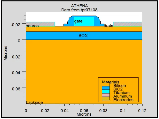
[image:19.595.155.483.484.730.2]The partial depleted (PD) instead of fully depleted (FD) SOI has become the desirable choice for mainstream digital applications, due to the ease of manufacturing, better control of short channel effects, larger design window for the threshold voltage, and lower self heating effect [1]. The figure 1.1 shows the physical structure device of UTB SOI. Further study, to see the impact of different titanium gate thickness on the UTB SOI performance.
3
1.2 Objective
The objectives of this project are:
1. To design Ultra-Thin Body SOI of the 22nm N - MOSFET.
2. To investigate the performance of 22nm N-MOSFET Ultra-Thin Body SOI including IV characteristic, leakage current, drive current, and subthreshold slope.
3. To compare the thickness of titanium (Ti) metal gate from 5nm, 10nm, 15nm, 20nm and 25nm at 22nm gate length.
1.3 Scope
i. Focus on the ultra-thin body SOI for 22nm N-MOSFET.
ii. Simulation tools using SILVACO to get the result including IV characteristic, leakage current, drive current, and the sub-threshold slope.
1.4 Problem Statement
The low switching energy of silicon on insulator technology still occur which degrades the performance. Meanwhile, the conventional fully depleted SOI MOSFETs have worse short-channel effect than bulk MOSFET and partially depleted SOI MOSFET. In words, short channel effects (SCE) decrease the threshold voltage, having extra leakage current between the source and drain degrade the performance of the device. The UTB utilizes metal gate may improve the performance ability to control the short channel effect with thin buried oxide (TBO).
4
The advantage used the SOI technology is reducing the SCE and improve performance. In ultra-thin body SOI (UTB SOI) with the adoption of high-k/metal technique are also being developed that acts on performance on of limitation of mobility. The usage UTB SOI can suppress SCE, scale gate length and also can reduce sub-threshold gate leakage current. In addition, UTB transistor does not rely on body doping to provide a potential barrier between the source and drain.
1.5 Thesis Guideline
In this thesis contains five chapters, Chapter 1- introduction of the research study, Chapter 2- literature review, Chapter 3- methodology, Chapter 4- result and discussion, and Chapter 5- Conclusion.
Chapter 1, the introduction of this project include the objective, scope, background of this project, and a problem statement.
Chapter 2, is presented the literature review consist of introducing to the scaling MOSFET theories using the ITRS demand, performance of the I-V characteristic, leakage current, short channel effect between source and drain, drive current and actual graph of sub-threshold slope.
Chapter 3 will be elaborate the design process simulation using SILVACO software whereby, Athena is used for writing the coding to build the structure of MOSFET and Atlas used for displaying the graph.
Chapter 4, discussion and analysis of the result, finding including an explanation of the problem occur when during the simulation. Investigate the result have been done in detail to optimize the performance the MOSFET.
5
1.6 Conclusion
CHAPTER 2
LITERATURE REVIEW
[image:23.595.203.432.340.490.2]2.1 Introduction
Figure 2.1: N- channel Mosfet (NMOS) Structure [2]
A MOSFET shows at figure 2.1 consists of an n- (p-) doped silicon substrate with two, highly p-(n-) doped contacts, source and drain. The channel region in between is covered by an insulator layer, the gate-oxide, which is in contact with the gate electrode. Without applying a voltage at the gate electrode, no current can flow from source to drain as the pn-junctions between each contact and the substrate act as two opposite diodes. [2]
7
In addition, the central to the functionality is the thin insulating layer, the gate oxide. The gate oxide acts as the dielectric of a capacitor which attracts charge carriers into the channel region. Up to now, silicon dioxide (SIO2) has been used as a gate oxide. Two so far unparalleled electrical and structural properties of silicon’s native oxide are commonly known as window glass are said to be one of the main reasons that silicon is today’s semiconductor of choice. [2]
2.2 Bulk MOSFET/ Conventional MOSFET
[image:24.595.156.479.436.612.2]The Metal-Oxide-Semiconductor has four terminal device which are drain (D), gate (G), source (S); and body (B) terminals. In addition, the channel region from drain and source, whereby they are connected to the inversion layer. The channel length (L) place between the source and drain channel, while the channel width (W) from in the direction normal to the channel length [3]. Below is the illustration of MOSFET structure.
Figure 2.2: The P MOSFET structure [3]
In the depletion mode of MOSFET, to construct of n-channel mosfet there is two highly doped n regions are diffused into a p-type substrate and represent the source and drain [4].
N Type N Type
![Figure 2.1: N- channel Mosfet (NMOS) Structure [2]](https://thumb-ap.123doks.com/thumbv2/123dok/496971.55461/23.595.203.432.340.490/figure-channel-mosfet-nmos-structure.webp)
![Figure 2.2: The P MOSFET structure [3]](https://thumb-ap.123doks.com/thumbv2/123dok/496971.55461/24.595.156.479.436.612/figure-the-p-mosfet-structure.webp)
