4GHZ LOW NOISE AMPLIFIER FOR SATELLITE DOWNLINK COMMUNICATION
NORNABILA BINTI MD NOR
This Report Is Submitted In Partial Fulfillment Of The Requirements For The Award Of Bachelor Of Degree Electronic Engineering (Telecommunication Electronic)
With Honors
Faculty of Electronic Engineering & Computer Engineering Universiti Teknikal Malaysia Melaka
ii
UNIVERSTI TEKNIKAL MALAYSIA MELAKA
FAKULTI KEJURUTERAAN ELEKTRONIK DAN KEJURUTERAAN KOMPUTER
BORANG PENGESAHAN STATUS LAPORAN
PROJEK SARJANA MUDA II
Tajuk Projek : 4GHZ LOW NOISE AMPLIFIER FOR SATELLITE DOWNLINK COMMUNICATION
Sesi
Pengajian : 1 3 / 1 4
Saya NORNABILA BINTI MD NOR
mengaku membenarkan Laporan Projek Sarjana Muda ini disimpan di Perpustakaan dengan syarat-syarat kegunaan seperti berikut:
1. Laporan adalah hakmilik Universiti Teknikal Malaysia Melaka.
2. Perpustakaan dibenarkan membuat salinan untuk tujuan pengajian sahaja.
3. Perpustakaan dibenarkan membuat salinan laporan ini sebagai bahan pertukaran antara institusi pengajian tinggi.
4. Sila tandakan ( √ ) :
SULIT*
*(Mengandungi maklumat yang berdarjah keselamatan atau kepentingan Malaysia seperti yang termaktub di dalam AKTA RAHSIA RASMI 1972)
TERHAD** **(Mengandungi maklumat terhad yang telah ditentukan oleh organisasi/badan di mana penyelidikan dijalankan)
TIDAK TERHAD
Disahkan oleh:
__________________________ ___________________________________
iii
” I, hereby declare that this report is the result of my own work except for quotes as cited in the references.”
iv
“I hereby declare that I have read this report and in my opinion this report is sufficient in terms of the scope and quality for the award of Bachelor of Electronic
Engineering (Telecommunication Electronic) with Honors”
Signature : ....………
v
For the most beloved and supporting parents,
MD NOR BIN HJ ALIAS
ROPE’NGAH BINTI JANTAN
vi
ACKNOWLEDGEMENT
Alhamdulillah, all praise to Allah SWT, God Almighty, Most Merciful for His guidance, blessing and by his will the project is successfully finished. A million thanks to my beloved family, who gives me encouragement and moral supported throughout the project. Without the encouragement and moral supported , the project will not be succeeded. Their trust and conviction towards me will always inspire me to become honestly in knowledge and never give up whatever happened towards especially during realization this final project. It is to them that I dedicate this work.
Generally, I personally gratitude to my supervisor; Dr Mohd Azlishah Bin Othman for His wide knowledge and critical thinking has helped me in a lot of way in completing this project. This project is done by his guidance and supervision and he has helped me understand the task at hand that has to be done.
vii
ABSTRACT
viii
ABSTRAK
ix
TABLE OF CONTENTS
CHAPTER TITLE PAGE
PROJECT TITLE STATUS REPORT FORM STUDENT DECLARATION SUPERVISOR DECLARATION ACKNOWLEDGEMENT ABSTRACT ABSTRAK TABLE OF CONTENTS LIST OF TABLE LIST OF FIGURES LIST OF APPENDICES
i ii iii iv vi vii viii ix xiii xiv xv I INTRODUCTION
1.1 Project Background 1.2 Problem Statement 1.3 Objective 1.4 Scope of Project 1.5 Thesis Outline 1 1 2 3 4 4 4
II LITERATURE REVIEW
2.1 Satellite Frequency Bands 2.2 Satellite Communication 2.3 Low Noise Amplifier 6
x
2.4 Transistor 2.5 Conclusion
10 12
III METHODOLOGY
3.1 ATF54143
3.2 Project Planning 3.3 Design Specification 3.4 Design Architecture 3.5 Process Design Flow 3.6 Design Low Noise Amplifier 3.6.1 DC Bias Network 3.6.2 S-parameter 3.6.3 Two Port Network
3.6.4 Stability 3.6.5 Noise Figure
3.6.6 Input and Output Matching 3.6.6.1 Single Stub Matching 3.7 Advance Design System (ADS 2011) 3.8 Fabrication Process 3.9 Measurement Setup 3.10 Performance Trade-off in LNA design 3.11 Conclusion
13 13 14 15 15 17 17 19 19 21 22 23 24 25 26 27 29 30 31
IV RESULTS AND DISCUSSION
4.1 S-parameter 4.2 Stability
4.3 Reflection Source (Γs ) and Reflection Load(ΓL)
4.4 Reflection Coefficient at the input and output 4.5 Gain
4.5.1 Power Gain 32 32 33 33 33 34 34 4.5.2 Transducer Power Gain 4.5.3 Available Power Gain
xi
4.6 LNA Simulation Results 4.6.1 Stability
4.6.2 DC Biasing
4.6.3 Input and output matching 4.7 Schematic View of LNA design
4.7.1 Circuit Description 4.7.2 S-parameters result 4.7.3 Performance summary of LNA 4.8 Layout of LNA Design
4.8.1 Layout consideration 4.8.2 DRC and LVS 4.9 Prototype Fabricated
4.10 Discussion 4.11 Conclusion
35 35 36 39 41 41 42 43 45 45 46 46 47 49
V CONCLUSION AND FUTURE WORK
5.1 Conclusion 5.2 Future Work
REFERENCES
Appendix A: Input Matching Smith Chart Appendix B: Output Matching Smith Chart Appendix C: ATF-54143 Data Sheet
xii
LIST OF TABLE
NO TITLE PAGE
2.1 Bands available for fixed satellite 7
2.2 CMOS vs PHEMT 9
3.1 Stability and criteria of transistor 22
4.1 S-parameters at 4GHz from simulation 32
4.2 Comparison Before Matching and After Matching 44
4.3 Comparison between design target and simulation 44
xiii
LIST OF FIGURE
NO TITLE PAGE
2.1 The microwave spectrum 7
2.2 Basic block diagram of RF 9
3.1 Gantt Chart 14
3.2 Flowchart of Project methodology 16
3.3 General flow of low noise amplifier design 18
3.4 LNA block diagram 18
3.5 S-parameter representation of two-port network diagrams 20
3.6 Two-port network diagrams 21
3.7 Stability of two-port networks 22
3.8 Single-stub matching circuits (a) Shunt stub; (b) Series stub 26 3.9 Advance Design System 2011 27
3.10 Fabrication Process; (a)LNA print layout; (b) UV Exposure unit ; (c) Etching machine; (d) Stripping machine (a)27; (b);(c);(d)28 3.11 Setup equipment testing 29
3.12 Trade-off of LNA design 30
4.1 Stability of design 36
4.2 Voltage divider biasing 37
4.3 Voltage divider with lumped componen 37
4.4 (a)Transistor tested by using curve trace ; (b) IV characteristics of the transistor 38
xiv
4.6 Stability 42
4.7 Input reflection(S11) and Output reflection(S22) 42 4.8 S12(isolation) and S21(gain) simulation results 43
4.9 Noise figure(nf2) simulation results. 43
xv
LIST OF APPENDICES
NO TITLE PAGE
A Input Matching Smith Chart 53 B Output Matching Smith Chart 54 C ATF-54143 Data Sheet 55
1
CHAPTER I
INTRODUCTION
1.1 Project Background
2
Low Noise Amplifier is one of the RF Receiver links that functioned to amplify the received signal in front end receiver especially. Initially, Low Noise Amplifier is one of the key components used to dominate the sensitivity of the complete receiver. The received signal might be very weak and the Low Noise Amplifier used to amplify the signal without injects much noise from the Low Noise Amplifier itself. This LNA is usually placed close to the detection device (antenna) to reduce losses and to avoid degradable of the signal-to-noise ratio (SNR). A good Low Noise Amplifier adds as little noise as possible to the signal and has high gain. Since the satellite downlink receiver operating with frequency 4GHZ (received signal) is weak, the LNA design to provide major gain with minimum the noise that flow to the system and boost the antenna signal.
The selective transistor is necessary it to calculate the value of s-parameters before simulation done. The s-parameters use to match impedance for minimum noise figure because s-parameters use for high frequency circuit. At last but not least, this report will force designer to design complexity the schematic and layout of LNA. To design LNA some parameter highlighted includes noise , input output matching, stability, linearity and gain that which will affect the performance of the entire receiver.For this project, the LNA are design by using a ATF54143 transistor from Avago Technologies and simulated by using Advance Design System 2011 software by Agilent Technologies. This project will deals mostly with Low Noise Amplifier design, fabricating and testing the amplifier using Vector Network Analyzer.
1.2 Problem Statement
3
much advantage compare to the passive biasing circuit.The only improvement detected and recorded is the noise figure performance of the Low Noise Amplifier with active biasing circuit. The matching networks using microstrip stub element matching is easier to design, simple and cost savings compare to two other matching. By using high performance devices such as the ATF-54143, however, circuits designed on FR4 material can meet the customer‟s requirements for noise figure, gain and linearity. The biggest benefit to customers is the lower cost of the FR4 material. This is a critical concern for customers‟ main production.
1.3 Objective
There are several objectives during designing this Low Noise Amplifier. The objectives include:
1. To study the characteristic and the specification of low noise amplifier (LNA) for satellite communication at 4GHz.
2. To design and simulate a low noise amplifier by using Advance Design System 2011.
4
1.4 Scope of Projects
The scope of project is explore varies topologies of low noise amplifier and identify the most suitable method to satisfy the design target. Scope of this project can be separated into three parts:
1. Simulation-It will be done by varied parameters using Advanced Design System (ADS) in order to get required results which are close to the theoretical results.
2. Fabricating-The fabrication of the Low Noise Amplifier, PCB laminate (e.g:FR4 board), components, etching facilities.
3. Test analysis-A test analysis is the last stage in this project. The performance of the designed amplifier circuit is verified on board using RF testing equipment such as the vector network analyzer and cable.
1.5 Thesis Outline
The thesis is divided to five chapters and covers covering the research works that have been through for Low Noise Amplifier circuit design.
1. Chapter 1 is introduces the concept of the project, which is a brief the introduction for the satellite and Low Noise Amplifier. Several objectives are made to achieve the designing LNA.
5
3. Chapter 3 describes the design and simulation process and method that will be used. The transistor GaAS FET ATF54143 selected and Advance Design System 2011 used to simulate the LNA to obtain low noise figure and reasonable high gain.
4. Chapter 4 will report the simulation and measurement. This chapter also includes discussion from simulation and measurement results.
6
CHAPTER II
LITERATURE REVIEW
This Chapter will review the basic concept during designing Low Noise Amplifier circuit. Research has been done study include:
1) Satellite Frequency Bands 2) Satellite Communication 3) Low Noise Amplifier 4) Transistor
2.1 Satellite Frequency Bands
7
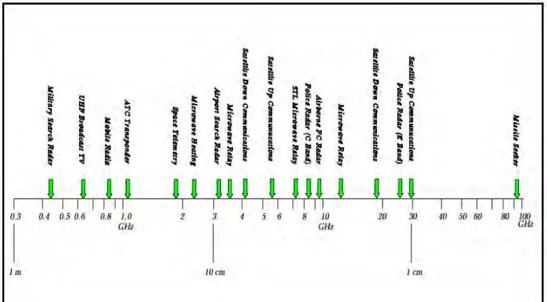
Figure 2.1: The microwave spectrum
[image:22.595.107.533.548.656.2]From the microwave spectrum, C band was the first part of the spectrum to be applied extensively to satellite communications and still extensively used due to the low cost and wide availability of components and avaibility in heavy rain compare to high frequency satellite.The Table 2.1 shows the RF Band frequency in satellite applications.
Table 2.1: Bands available for fixed satellite services
RF Bands Frequency(GHz)
L-Bands 1-2
C-Bands 4-6
Ku-Bands 12-18
8
2.2 Satellite Communication
S.Ekpo and D.George [3] in their journal have discussed of 4-8 GHz LNA Design for a Highly Adaptive Small Satellite Transponder Using InGaAS pHEMT Technology. Based on this journal, small satellite communication critical due to the noise level at the receiver. Thus, GaAs pHEMT consist of low noise and high gain in the frequency band 4-8GHz.A better design that delivers low noise performance, high gain and low power consumption for space mission. This LNA located in front receiver satellite successfully developed with high gain 17dB and 0.5dB of noise figure over the characterised bandwidth.
P.Raj Kumar [4], in this report have discuss and design of L-Band Low Noise Amplifier by using the ATF34143 GaAS HEMT’s.In His project, a discretely 2-stage L-band low noise amplifier designed with center frequency 1.25GHz.Next,GaAS HEMT’s offers low noise figure opposite to MESFET’s and silicon FET’s.This biasing sections by using radial stubs matching with tapered line. This LNA successfully developed with high gain 20dB and noise figure 0.17dB.
Curtis L.Mayberry. [5] in his journal 6GHz Low Noise Amplifier Design for C band application lies in the IEEE. This band suitable for satellite communications. This LNA design by using transistor pHEMT GaAS FET and operate at 6GHz.This amplifier need a high gain to effectively amplify the small signals received and to reduce noise. This amplifier successfully design and fabricated by using Duroid RO30006 with reasonable gain 13.1dB and noise figure 0.81dB.
2.3 Low Noise Amplifier
9
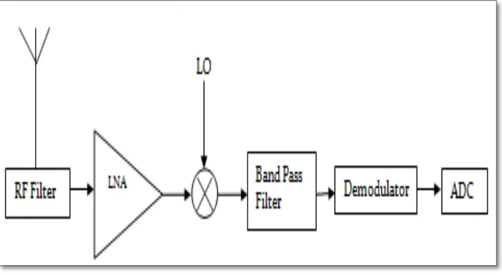
[image:24.595.136.502.215.416.2]After that, RF filter then act with the LNA and this is where LNA function to amplify the signal before sent to the mixer. The signal with a local-oscillator (LO) and band pass filter [6] will combine by the mixer. Mixer used to amplify small signal or generate large signal. The signal will demodulate by demodulator, and then it will apply to ADC. The affected the performance of LNA especially at receiver are the case sensitivity for noise parameters [6].
Figure 2.2: Basic block diagram of RF