CHIPPING FREE PROCESS FOR COMBINATION OF NARROW SAW STREET (60UM)
AND THICK WAFER (600UM) SAWING PROCESS
by
1
Mohd Syahrin Amri, Senior Instructor Engineer
2David Liew, Development Engineer
2Fuaida Harun , Senior Development Manager
I Universiti Teknikal Malaysia Melaka
Hang Tuah Jaya, 76100 Durian Tunggal 76100 Melaka Malaysia Phone: +606-555 2181, Fax: +606-331 6247,
Email: [email protected]
2Inineon Technologies (Advanced Logic) Sdn Bhd Batu Berendam FTZ, 75350 Melaka Malaysia
Phone: +606-232 8718, Fax: +606-251 8140
ABSTRACT
Chipping ree is a dream for wafer sawing process. With current high complexity of wafer technology plus the drive for cost reduction by narrowing the saw street width, it is a challenge which requires huge effort for wafer sawing process to achieve chipping ree process. Higher density of metallization causing higher blade loading during mechanical sawing. This leads to chipping penetrating under the guard ring and damaging the active area. This paper will share all the activities towards chipping ree process on a device involving optimization through mechanical sawing, inra red camera and laser grooving process. Blade selection involving various diamond grit size, different concentration, slit design and low k types only able to minimize the occurrence but not totally eliminate it. Finally by performing laser grooving, signiicant results were achieved with zero chipping occurrences. In addition, suitable laser requency selection is also important to ensure the best perfomance. In this case higher requency laser grooving in combination with mechanical sawing process found to be able to meet the requirement.
Keyword - chipping/peeling ree, seal ring, laser grooving
1. INTRODUCTION
Wafer sawing is a cutting process which separate dies rom a piece of wafer. The sawing process can be done by mechanical or laser process. The area that has been cut away during sawing process is called sawing street. On sawing street, chipping or peeling level is the key factor to determine the quality of the unit. Once the chipping/ peeling entering the guard ring or circuit area, it will ruined the unction of the die itsel. In wafer sawing process, target always to minimize chipping but sawing without chipping is a dream for all engineers. There are a lot of efforts towards these activities which require a huge effort and rom this paper will share the activities done involving methods and parameter optimization.
This paper focus mainly on developing a sawing process with key objective to eliminate chipping or peeling from
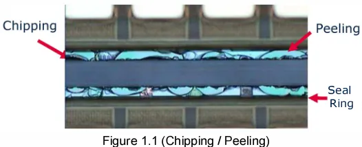
touching the seal ring. Chipping is deine when the sawing street structure or silicon material are totally removed while peeling criteria is a condition when only top layer portion being removed during sawing process. Further illustration could be referred in Figure l.l
Figure 1.1
(Chipping /
Peeling)
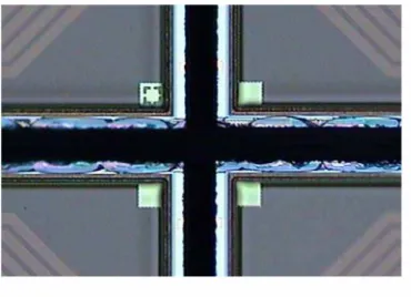
The key challenge for chipping/peeling ree process when existing of high density of Polyimide and PCM (Process Control Monitoring) structures on the sawing
street. Deinition of PoIyimide and PCM structures can be referred in igure 1.2.
Figure 1.2
The PCM structure contains hard metal such as Aluminium and Copper which may attached to the diamond blade and causing high blade loading during sawing. Higher peeling and chipping can be easily seen on this area compared to the clean area. This could be refer to igure 1.3.
Figure 1.3
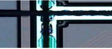
Once the blade loading is high it can cause scratch or chipping on the side wall as well. This occurred when the hard metal material stuck in between the diamond and rubbing with the sidewall area. However, so far the semiconductor industry has paid little attention to the fact that the same mechanism causing chipping is also responsible for inducing microcrack [2] This statement can be proven by referring to igure 1.4.
Figure 1.4
The sidewall scratches / chipping can introduced to quality issue whereby it can penetrate under the seal ring and destroy the chip unction by going into the active area. Though blade selection is very important in order to ensure the metal structure can be released easily during sawing and not stuck between the diamonds and caused sidewall scratches. The crack penetration can be seen in igure 1.5 below
Figure 1.5
In nonnal cases the peeling or chipping can be blocked by the seal ring and maintain the chip quality, however with the existing of sidewall scratches the quality issue becomes more complicated since the crack rom the sidewall scratches move under the seal ring and penetrate to active area.
cause blade wobbling. Blade wobbling resulting to
Before assessment starts machine had been calibrated and perpendicular check had been performed on chuck table. This is to ensure the machine is in good condition and to minimize variation. All blades during the assessment had been dressed using silicon wafer. Water temperature been ixed at 20°C ± 2°C during the assessment. For investigation purpose, a 600um wafer thickness with 8 inch wafer size had been selected with each samples 40 readings had been collected. Die size is ix to 5.13mm x 5.28mm dimension with 60um saw street width. For laser application, a coating will be applied to the wafer surface to protect the wafer surface rom any silicon particles contamination. The coating then will be removed during wafer cleaning process. Inspection will base on few quality sequence criteria. Firstly topside chipping / peeling will be inspected, if the result is good then will continue with sidewall chipping and lastly backside chipping inspection. If one criteria is fail, the next sawing process. For mechanical sawing Disco DFD6340 sawing machine was used and for laser sawing using sawing will continue rom the wafer back instead of ront side. This is to see the peeling or chipping performance when polyimide or metal structure is being sawn at last process. Further illustration could be refer to igure 1.6 and 1.7 for further understanding.
Figure 1.6 (Normal ront side sawing process)
Q
Figure 1.7 (Backside sawing using inra red camera)
In mechanical sawing assessments there were few activities conducted base on
1) sawing parameter optimization on cut depth, feedspeed and PM
2) blade type assessment which covered low k blade and slit blade
3) varies of diamond blade concentration and grit size 4) UV and Non UV mounting tape assessment 5) Surfactant involvement
6) Varies of cutting methods
7) Grinding towards thinner wafer thickness (standard 250um thickness)
3.2 Laser Sawing
Isolation cut
Pass 1 & 2
Pass 3 &4
Pass 5
5 passes of laser grooving
Figure l.8
4. RESULTS AND DISCUSSION
3.3 Mechanical Sawing
Cut through using mechanical dicing able to achieve peeling ree process. Cutting method base on single cut and step cut do not have signiicant impact. Parameter optimisation towards blade height, feedspeed and various blade RPM not able to achieve the set target. All assessment on mechanical approach involving different diamond grit size and diamond concentration also do not show any signiicant improvement towards peeling ree results. Nevertheless lower concentration and bigger grit size do reduced number of peeling occurrence on the sawing street. Lower feed speed and cutting height also reduce number of peeling however not able to eliminate it.
3.2 Laser Dicing
Laser dicing does provide results towards
peeling ree process. However laser frequency selection is very important in order to achieve the desired target. Base on assessment made, low requency laser not able to provide good results and the performance is comparable with the mechanical sawing. High requency laser does bring signiicant impact and provide positive results in the assessment. Even with combination with mechanical sawing on the second cut still manage to provide
convincing peeling free process. Figure 1.9 and Figure
2.0 are the comparison results between mechanical and high requency laser sawing.
Figure 1.9
(Mechanical sawing only, peeling observed)
Figure 2.0
(High Frequency laser and mechanical sawing, No peeling observed)
Below are results summary base on activities evaluated to achieve chipping / peeling ree process
No Assessment Method Peeling free
1 Blade height assessement ranging from 5um to -ve
190um of wafer thickness on first cut
2 Fedspeed assessment from 1 mm/s up to 100mm/s -ve
3 Cutting methd single and stepcut -ve
10 Reduce wafer thicness from 600um to 250um -ve
11 Low Frequency Laser -ve mechanical sawing as a sawing method. It is important to use step cut during sawing and ensure that the irst cut using high requency laser application. This is to ensure the metallization on sawing street to be removed without any peeling/chipping occurrence. Since laser sawing has limitation to cut thick wafer, it is require using
mechanical sawing as the 2nd cut. With this combination,
base on 60um kerf and 600um wafer thickness criteria for chipping/peeling ree process.
6. ACKNOWLEDGEMENTS
The authors wish to acknowledge Disco, KNS and all Inineon team members (especially David Liew and Fuadia Harun) for their supportive role in making of a successful project.
7. REFERENCES
[1] Gatzen HH: Investigations Regarding The Operating Range OfUItra Grinding Wheels on Altics, page 1
[2] Gatzen HH: Dicing challenges in microelectronics and micro electro-mechanical systems (MEMS), page 1