DOI: 10.12928/TELKOMNIKA.v15i1.4749 125
Investigation Study of Three-Level Cascaded H-bridge
Multilevel Inverter
Mohd Ruddin Ab Ghani1*, Nabil Farah2,Jurifa Lazi3, M.R.Tamjis4, Md Nazri Othman5, Nur Huda Mohd Amin6, Syariffah Othman7, Zanariah Jano8, Tole Sutikno9
1,2,3,4,5,6,7Faculty of Electrical Engineering (FKE), 8
Centre for Languages and Human Development
1,2,3,4,5,6,7,8Universiti Teknikal Malaysia Melaka, Hang Tuah Jaya, 76100 Durian Tunggal, Melaka, Malaysia. 9
Department of Electrical Engineering, Faculty of Industrial Technology, Universitas Ahmad Dahlan (UAD), Jln Prof. Dr. Soepomo, Janturan, Yogyakarta 55164, Indonesia
*Corresponding author, email: [email protected]
Abstract
This paper analyzed three-level Cascaded H-bridge Multilevel Inverter (CHMLI) utilizing two modulation techniques namely Sinusoidal Pulse Width Modulation (SPWM) and Space Vector Pulse Width Modulation (SVPWM). The performance and the output of CHMLI in terms of Total Harmonic Distotion (THD) % and circuits complexity were compared. The simulations models were constructed using MATLAB/SIMULINK. The results showed the CHMLI produced the lowest THD contents and utilized fewer components. Moreover, the SVPWM produced less THD than SPWM.
Keywords: CHMLI, cascaded, MATLAB/SIMULINK, SPWM, SVPWM, THD, inverter
Copyright © 2017 Universitas Ahmad Dahlan. All rights reserved.
1. Introduction
In the past few years, numerous research and experiments have been conducted in power electronic field in order to obtain renewable energy resources that have less impact on environment to replace the common widely used foil-based resources which produce harmful effects to the environment and the planet [1, 2]. Most existing renewable energy resources are Direct current (DC) in nature such as solar energy and wind energy. These DC energies often require conversion to Alternative current (AC) in order to be used in daily life applications which are AC energy-based. An inverter is a device that is able to convert the DC energy into AC energy by utilizing some power electronic components [3]. However, in real life, most inverters are not capable of handling high power applications because they are mainly designed for low power applications. Hence, DC energy should be produced from renewable resources to handle high power applications. A multilevel inverter which is capable of handling small and high power application with less harmonic contents in its output should be designed [4].
In the recent few decades, a multilevel inverter has been the main focus for most researchers in the power electronic field due to its ability to deal with medium and high power application besides various advantages it offers when comparing it to the conventional two level inverter operating at the same rating. The multilevel inverter produces less harmonic contents in its output voltage and current. In addition, the power switches in multilevel inverter experience low voltage stress and low electromagnetic interferences (EMI) [4].
The concept behind multilevel inverter is that it uses numerous combinations of power electronic switches to produce staircase waveform where as much as the level increases the output waveform become almost sinusoidal with low harmonic in it is output waveform [7]. Multilevel inverter topologies can be arranged in many different combinations, among the popular multilevel inverter topologies are Diode Clamped Multilevel Inverter (DCMLI), Flying Capacitor Multilevel Inverter (FCMLI) and Cascaded H-bridge Multilevel Inverter (CHMLI). All these topologies have their own combinations and features. The first multilevel topology is the Cascades H-bridge design as shown in Figure 1 which implements a set of H-bridge separate dc source inverter serially connected to produce an n-voltage level. This is followed by the diode clamped inverter as shown in Figure 2 which utilizes bank of series capacitor paralleled with dc source to produce an n-additional voltage sources. Another multilevel topology subsequently introduced is the flying capacitor design as shown in Figure 3 in which the capacitors are floating rather than series-connected. Moreover, there are different multilevel designs which involve parallel connection of inverter phases through inter-phase reactors [7].
At present, most researchers and manufacturers in power electronic field are interested in a multilevel inverter due to its advantageous in terms of harmonic reductions, better waveform output and better medium and high power applications handling [8].
Figure 1. Three-phase 3-level CHMLI Figure 2. Three-level single phase DCMLI
Figure 3. Three-level single phase FCMLI
(Figure 4). Different modulation techniques and the results of conventional two-level inverter and other multilevel topology (DCMLI, FCMLI) are presented [10].
Figure 4. Block Diagram of the Research
2. Basic Principle Cascaded H-Bridge Multilevel Inverter
The cascade H-bridge multilevel inverter consisted of a number of single full bridge inverter units. Each bridge was fed by separate dc source namely battery, PV cell or any kind of dc supply. The output of each bridge could be summed up to generate almost sinusoidal output voltage waveform for nth level of CHMI each full bridge inverter unit forming the CHMI with separate dc. Four semiconductors switches are able to produce three different voltage levels namely +vdc, 0 and –vdc depending on the switching state. Each of the switching always conducts for 180 degree or half-cycle regardless of the pulse width of the quasi-square wave so that this method will result in the equalization of the current stress in each of the components [7].
Figure 5. Three level CHMLI Figure 6. Staircase voltage waveform for Single-phase multilevel inverter [11]
Figure 5 shows a three-level of CHMI. Each H-bridge was activated at certain amount of time at different start up angle and because each bridge was fed by separate dc source, the output of all the bridge which formed the CHMI output would be the sum of the separated dc sources for three phase nth level of CHMI inverter. An output equation used is as follows:
(1)
(2)
From the equations above, it can be concluded that the output voltage of cascaded H-bridge multilevel inverter was the sum of the separated dc sources across the multilevel inverter. The Fourier series of bridge multilevel voltage waveform as in Figure 6 can be expended as shown in equation 4 [11].
∑ (4)
For equal and constant source the bn is given by:
∑
(6)
Where,
L= the number of dc sources for each full bridge inverter cell N= the number of switching angles
The total harmonic distortion (THD) is a method to calculate the total distortion in the output waveform caused by the harmonics presence in the output. A general equation of the total harmonic distortion (THD) is given as follows [2]:
√∑ ∑ ∑
(7)
3. Modulation Techniques
In terms of the control strategy of a multilevel inverter, numerous researchers in the power electronic field have developed many modulation techniques. The two famous and simple modulation techniques are the Sinusoidal Pulse Width Modulation (SPWM) and, the Space Vector Pulse Width Modulation (SVPWM). A multilevel inverter switching signal can be generated using these two methods with less switching losses and harmonic distortion.
3.1. Sinusoidal Pulse Width Modulation (SPWM)
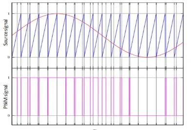
The CHMI was controlled by the SPWM where sinusoidal wave was compared with square waves to generate the switching signal that would trigger the semiconductors switches in time sequence considering the phase between the phases shift three phase inverter legs. This method used N-1 level carrier signals to generate the N-level inverter output voltage. In multilevel inverter, the frequency modulation index, and the amplitude modulation index, is defined as follows [12, 13]:
(8)
(9)
Where = carrier signal frequency, = reference signal frequency, = carrier signal amplitude, = reference signal amplitude.
into two regions to fit the reference sine wave amplitude. Figure 7 and 8 show the SPWM carriers signal compared with reference sinusoidal signal for 2-level and 3-level inverter.
Figure 7. The SPWM carriers signals of 2-level inverter
Figure 8. The SPWM carriers signals of 3-level inverter
3.2. Space Vector Pulse Width Modulation (SVPWM)
Space Vector Modulation (SVM) is an algorithm for the control of pulse width modulation (PWM). The idea behind SVPWM is to create a rotating space vector that will be used for various applications. One method to be used in inverter was the switching times.
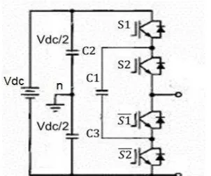
The circuit in Figure 9 demonstrates the foundation of a two-level voltage source converter. It had six switches (sw1-sw6) and each was represented by an IGBT switching device. A, B and C represented the output for the phase shifted sinusoidal signals. Depending on the switching combination, the inverter would produce different outputs, creating a two-level signal. The biggest difference from other PWM methods was that the SVPWM used a vector as a reference. This offers a better overview of the system [14].
Figure 9. The two level voltage source inverter with its voltage vectors
3.2.1. References Vector
The reference vector was represented in a αβ-plane. A two-dimensional plane was
transformed from a three-dimensional plane containing the vectors of the three phases. The ON
or OFF switch was determined by the location of the reference vector on this αβ-plane
(Figure 10).
The space vector of a three-level inverter is shown in Figure 11. It was composed of six space vector diagrams of two-level inverter. Each space vector of two-level inverter was
Figure 10. The references vectors for sector 1 and the reference vector in all sector
Figure 11. The three-level inverter Figure 12. The 3-level inverter voltage vector
3.2.2. Derivation of Reference Voltage
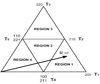
SVPWM method of three-level inverter is similar to that of Conventional two-level SVPWM in principle. Hence, various techniques which are used in two-level SVPWM, can be adopted to this method. Figure 12 shows the space vector simplification of three-level inverter [15].
The space vector of three-level inverter can be simplified to that of two-level inverter. The number in Figure 13, represented as s, is the index that denotes the six small hexagons, constituting the three-level space vector diagram. Regions exist which are shared by adjacent small hexagons in the three-level space vector diagram [15].
Figure 13. Dividing sector into four triangular regions
3.2.3. Total Harmonic Distortion (THD)
presented in the output voltage or current waveform which causes the waveform to be distorted and does not produce a pure sinusoidal signal. The harmonic distortion is produced due to the components of the inverter and control strategy used to trigger the inverter semiconductors switches. The harmonics distortion, hence, needs to be investigated and analyzed in order to propose a method to reduce these distortions.
√ (10)
Where:
THD= Total harmonic distortion = Fundamental Voltage magnitude = Magnitude of 2nd Harmonic = Magnitude of 3rd Harmonic = Magnitude of nth Harmonic
In the case of multilevel inverter which produces stepped waveform, another accurate formula to calculate the THD is proposed which utilizes the switching angle of the wave form as shown in equation 11.
√∑ (11)
Where:
is the amplitudes of the fundamental component, whose frequency is And is the amplitudes of the nth harmonics at frequency
4. Simulation Results
To verify the theoretical analysis, three-level CHMLI was constructed using SPWM and SVPWM. A conventional two-level inverter and two other topologies of 3-level inverter (DCMLI, FCMLI) were also constructed and presented along with their simulation results for the purpose of comparison and illustration of preference and superiority of CHMLI among other topologies as well.
Figure 14 and 15 show the conventional two level inverter circuit controlled by SPWM and SVPWM.
Figure 14. The two level inverter circuit and its gating signal (SPWM)
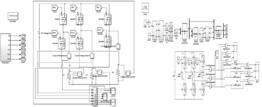
Figure 16 and 17 show the three-level inverter controlled with SPWM and SVPWM along with the modulation circuits. Figures 18 and 19 show the three levels inverter DCMLI and FLCMLI.
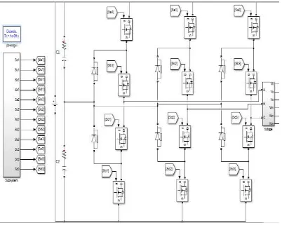
Figure 16. Three level cascaded h-bridge multilevel inverter with its control signal
(SPWM)
Figure 17. Three level inverter using SVPWM
Figure 18. Three level diode clamped multilevel inverter with its control circuit
Figure 19. The three level flying capacitor with its control circuit
4.1. Cascaded H-bridge Multilevel Inverter
Figure 20. Comparison of carrier with reference sine wave for two-level inverter
Figure 21. Output line voltage of two level inverter using SPWM
Figure 22. THD of line voltage of two-level inverter with SPWM
While Figure 23 shows the output line voltage of two-level inverter using SVPWM. Figure 24 shows the THD analysis of line voltage of two-level inverter with SVPWM.
Figure 23. Output of line voltage of two-level inverter using SVPWM
Figure 24. THD of line voltage of 2 level inverter using SVPWM
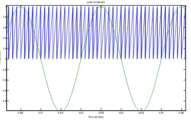
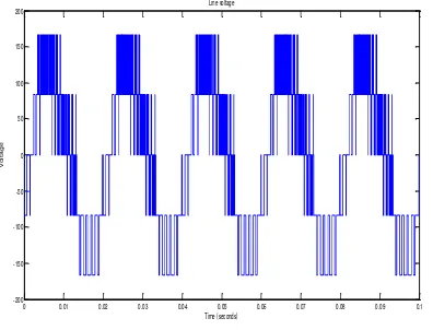
For three-level inverter, Figure 25 shows a comparison between carrier signals and references signal for three-level inverter. Figure 26 shows the output line voltage of three level inverter using SPWM and Figure 27 shows the THD analysis of three level inverter using SPWM as well.
0.005 0.01 0.015 0.02 0.025 0.03 0.035 0.04 0.045
-0.8 -0.6 -0.4 -0.2 0 0.2 0.4 0.6 0.8 1
Time (seconds)
A
m
p
il
tu
d
e
Figure 25. Compression of carrier signal against reference signal
Figure 26. Output current of three-level inverter using SPWM
Figure 27. THD of three level inverter output current using SPWM
In addition, the three-level inverter has been modeled using SVPWM. Figure 28 shows the output line voltage of three-level inverter using SVPWM and Figure 29 shows the THD analysis of three-level inverter with SVPWM as well.
Figure 28. The output of line voltage of three-
Figure 30. Output line voltage of three-levels DCMLI using SPWM
Figure 31. THD of line voltage of three-level DCMLI
5. Results Analysis
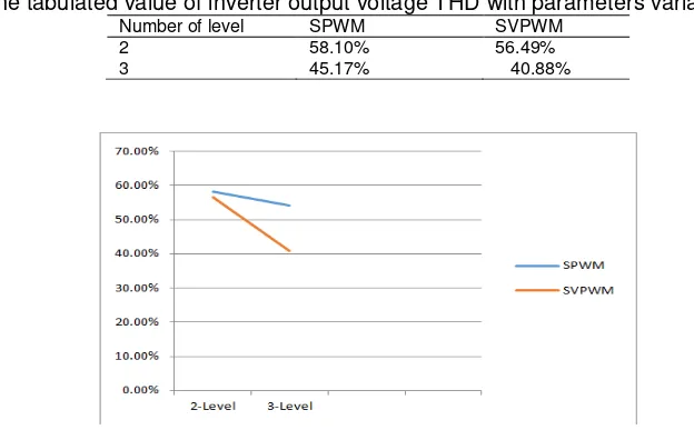
Table 1 shows the tabulated value of inverter output Line voltage THD with respect to the number of output levels of CHMLI (Cascaded H-bridge Multilevel Inverter).
Table 1. The tabulated value of inverter output voltage THD with parameters variation
Number of level SPWM SVPWM
2 58.10% 56.49%
3 45.17% 40.88%
Figure 32. THD Analysis
The THD value is tabulated in Table 1 and the graph in Figure 33. The THD of the inverter was reduced if the inverter was controlled using space vector pulse width modulation. A reduction from 45.17% when using sinusoidal pulse width modulation (SPWM) to 40.88% when using the SVPWM was observed, indicating that the Space vector modulation technique is the best solution in terms of output voltage, harmonic losses and number of switching per cycle.
As the aim of this paper was to propose different multilevel inverter topologies and compare them in terms of different aspects, Table 2 shows the comparison among the three MLI topologies.
Table 2. Comparisons between MLI topologies
Inverter type No.level Carrier frequency THD% Modulation techniques
CHMLI 3 10000 45.17% SPWM
DCMLI 3 10000 46.99% SPWM
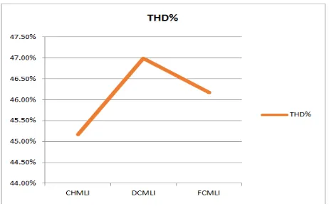
Figure 33 shows the THD % graph for three different multilevel topologies. Hence, the CHMLI has the lowest THD% among the topologies. Table 3 shows the comparison between MLI topologies in terms of components used for three-level inverter.
Figure 33. THD Analysis Graph
Table 3. Number of Components used in Each MLI Topology
Inverter type Number of switches Numbers capacitors Number of diodes Total of components
CHMLI 12 0 0 12
DCMLI 12 2 6 20
FCMLI 12 12 0 24
Based on the information tabulated above and the THD curve, the CHMLI has the best THD% compared to other topologies. Besides, it utilizes the fewest semiconductors devices where it neither requires any clamping diode nor balancing capacitor. In addition, the CHMI is the easiest topology in terms of circuit complexity especially when implementing higher inverter levels.
6. Conclusion
This present study has investigated three-level inverter, focusing mainly on Cascaded H-bridge Multilevel Inverter (CHMLI) by utilizing two modulation techniques namely Sinusoidal Pulse Width Modulation (SPWM) and Space Vector Pulse Width Modulation (SPWM). The paper compares the three-level CHMLI against conventional two-level inverter in terms of Total Harmonics Distortion (THD) with respect to different modulation techniques. Moreover, other multilevel topologies like (DCMLI and FCMLI) are included as well to compare them with CHMLI in terms of THD%, number of components used and circuits complexity. Hence, the findings yield that the CHMLI produces the lowest THD contents and utilizes fewer components. Moreover, the SVPWM produces less THD than SPWM.
Acknowledgements
The authors would like to gratefully acknowledge the funding support provided by Universiti Teknikal Malaysia Melaka (UTeM) under the research grant No: PJP/2016/FKE/HI5/S0148/Malaysia, UTeM.
References
[1] Colak Ilhami, Ersan Kabalci, Ramazan Bayindir. Review of multilevel voltage source inverter topologies and control schemes. Energy Conversion and Management. 2011; 52(2): 1114-1128. [2] Yiwei M, Ping Y, Hongxia G. Distributed generation system development based on various renewable
[3] Rahim NA, Saad Mekhilef. Implementation of three-phase grid connected inverter for photovoltaic solar power generation system. Power System Technology, 2002. Proceedings. PowerCon 2002. International Conference on. 2002; 4: 570-573.
[4] Tolbert Leon M, Habetler Thomas G. Novel multilevel inverter carrier-based PWM method. Industry Applications, IEEE Transactions on. 1999; 35(5): 1058-1107.
[5] Malinowski, Mariusz. A survey on cascaded multilevel inverters. Industrial Electronics, IEEE Transactions on. 2010; 57(7): 2197-2206.
[6] Gupta, Amit Kumar, Khambadkone Ashwin M. A space vector PWM scheme for multilevel inverters based on two-level space vector PWM. Industrial Electronics, IEEE Transactions on. 2006; 53(5): 1631-1639.
[7] Keith C. Operation and design of multilevel inverters. Developed for the office of naval research. 2003: 1-79.
[8] Prasad KNV, Ranjith Kumar G, Vamsee Kiran T, Satya Narayana G. Comparison of different topologies of cascaded H-Bridge multilevel inverter. Computer Communication and Informatics (ICCCI), 2013 International Conference on IEEE. 2013
[9] Nursyafiqah binti Zahari. Cascaded H - Bridge Multilevel Inverter. B.Eng Theses. Universiti Teknologi Malaysia; 2013.
[10] Minai, Ahmad Faiz, Abu Tariq. Analysis of Cascaded multilevel inverter. Power Electronics (IICPE), 2010 India International Conference on IEEE. 2010.
[11] Parkash Aman, Shimi SL, Chatterji S. Harmonics Elimination in Cascade Multilevel Inverters Using Newton-Raphson and Genetic Algorithm. International Journal for Scientific Research & Development (IJSRD). 2014; 2(5): 236-239.
[12] McGrath, Brendan Peter, Donald Grahame Holmes. Multicarrier PWM strategies for multilevel inverters. Industrial Electronics, IEEE Transactions on. 2002; 49(4): 858-867.
[13] Rueger Niklas E, Kuhn H, Mertens A. Harmonic distortion of multicarrier PWM strategies in cascaded multilevel converters with unequal DC sources. Power Electronics and Applications, 2007 European Conference on IEEE. 2007.
[14] Bengi T. Space Vector Pulse Width Modulationfor Three-Level Converters: a LabVIEW Implementation. Master Programme in Electrical Engineering. Sweeden: Uppsala Universitet. 2012. [15] Seo Jae Hyeong, Chang Ho Choi, Dong Seok Hyun. A new simplified space-vector PWM method for
three-level inverters. Power Electronics, IEEE Transactions on. 2001; 16(4): 545-550.