DOI: 10.12928/TELKOMNIKA.v14i4.3966 1263
Design of Single-Stage Flyback PFC Converter for LED
Driver
Wang Qi*, Wu Jie, Baohua-Lang
School of Electronic Information Engineering, Xi’an Technological University, Xi’ an, China *Correspponding author, e-mail: [email protected]
Abstract
A light emitting diode (LED) driver based on single-stage power factor correction (PFC) is presented in this paper. The designed LED driver using flyback topology can achieve power factor correction and constant-current drive LED in boundary conduction mode. The circuit principle is described in detail, the formulas for MOS switch-on time, switching frequency and the main impact factor of power factor are proposed. The experiment results show that the designed LED driver has high power factor, stable output and it can drive the LED with high efficiency.
Keywords: flyback, power factor correction, boundary conduction mode
Copyright © 2016 Universitas Ahmad Dahlan. All rights reserved.
1. Introduction
Light Emitting Diode (LED) called “green lighting” is the solid illuminant with many advantages, such as small size, high efficiency, long lifetime and no poison mercury content compared with the conventional fluorescent lamp. The Power Factor Correction (PFC) has been widely used to achieve low Total Harmonic Distortion (THD) and high Power Factor (PF) in LED driving power.
Many converter topologies can be used to drive the LED string, such as boost, buck-boost, SEPIC, flyback, half bridge converter and forward converter [1-4]. The flyback converter is the most commonly used topology for low power offline applications, especially when the isolation is necessary. LED lights drive by a constant current can be considered as a constant power load, and can work steadily at lower bandwidth. So when the output power is less than 100W, the flyback converter is a better solution for the LED driver.
The flyback converter can operate in continuous conduction mode (CCM), discontinuous conduction mode (DCM) and boundary conduction mode (BCM). The CCM and DCM operation modes for LED lamp applications have been discussed in several papers [5-9]. In the DCM operation mode, the single-stage flyback PFC converter can easily achieve unity power factor, however, the conduction loss, current stress, and voltage stress on the switch will significantly increase. Therefore, for high power applications, the continuous current mode (CCM) is suggested to achieve higher efficiency and higher power factor, but the control is more complex, and sometimes poor stability. In the BCM operation mode, the output rectifier diode of the flyback converter works under the Zero Current Switching (ZCS), thus improving the conversion efficiency of the converter. Meanwhile, the power factor correction can be achieved easily due to the linear relationship between the average input current and the input voltage. A large input filter used for eliminating the current harmonics in the DCM converter is unnecessary.
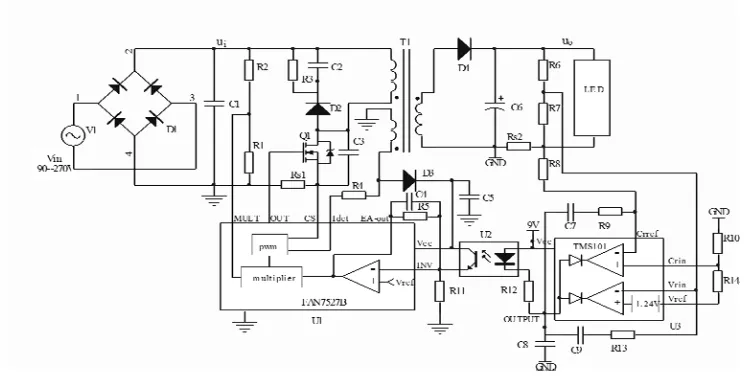
2. Principle analysis
Figure 1 is a flyback LED driver power supply circuit. Assume that the input line voltage is the ideal sinusoidal wave and the rectifier bridge is the ideal rectifier bridge, so the input voltage after rectifier bridge can be expressed as:
v ( )
int
v
pk
sin(2
f
Lt
)
(1)Where,
V
pkis the peak value of the line voltage, andf
Lis the frequency of the line voltage.Figure 1. LED driver based on Single-Stage Flyback PFC Converter
By adjusting the parameters of R5, R11 and C4 in the control circuit, the bandwidth of the control loop is lower than the frequency of the line voltage, so that in half power frequency cycle, the output of the error amplifier (EA-out) in the controller U1 is constant. The peak current of the transformer primary side is proportional to the line voltage after the rectification, and the original side peak current is a sine curve[10], expressed as:
( )
sin(2
)
pk pk L
i
t
i
f
t
(2)Assuming the turns ratio of the transformer is
n
, the efficiency is 1 and the winding is tightly coupled, so the peak current of the transformer secondary is:( )
( )
pks pk
i
t
n i
t
(3)The turn-on time of the switch Q1 is given as:
( )
sin(2
)
( )
sin(2
)
p pk p pk L p pk
on
in pk L pk
L i
t
L i
f
t
L i
T
v t
v
f
t
v
(4)Where,
L
p is the inductance of the transformer primary side. It can be seen from Equation (4) that the turn-on time of the switching is fixed under the condition of a certain input voltage and load.2
( ) ( / ) ( )
sin(2 )
( )
s pks p pk
off
o f o f
p pk L
o f
L i t L n n i t
T
v v v v
L i f t
n v v
(5)Where,
L
s is the inductance of the transformer secondary side,v
o is the output voltage of the converter, andv
f is the positive voltage drop of the output diodeD
4.If the circuit is working in boundary conduction mode, then the switching period of the switch is the sum of the turn-on time and the turn-off time, i.e.
T
T
on
T
off , so the duty ratio is:1 sin(2 ) 1 ( ) on pk L o f T D
v f t
T
n v v
(6)The switching frequency is:
1
1 sin(2 )
( )
pk s
pk
p pk L
o f
v f
T v
L i f t
n v v
(7)
It is observed that the switching frequency changes with the input voltage. When
sin(2
f
Lt
)
=0, the maximum switching frequency can be obtained nearby the zero crossing point of the line voltage.(max) pk s p pk
v
f
L i
(8)When
sin(2
f
Lt
)
=1, the minimum switching frequency can be get at the peak of the linevoltage. (min)
1
(
)
pk s pk p pk o fv
f
v
L i
n v
v
(9)Figure 2. LED power driver current waveforms in the boundary conduction operation mode
It is seen from Figure 2. that in the boundary conduction mode, the current waveform of the primary side in turn-on course is the triangular wave and the average current value of the primary side is half of the peak current, so the average current value can be obtained as:
sin ( 2 )
1
( ) ( )
2 2 1 sin ( 2 )
pk L
in pk
L
i f t
i t i t D
K f t
(10)
where,
(
)
pk
o f
v
k
n v
v
is the ratio of the peak voltage to the reflected voltage of thesecondary side. The smaller
k
is, the closer to the ideal sinusoidal wavei t
in( )
is and thehigher the power factor is. So theoretically, the flyback topology can achieve high power factor. Likewise, according to the current relationship between the primary side and secondary side, we can derive the current of the secondary side as:
2
sin (2 ) 1
( ) ( ) (1 )
2 2 1 sin(2 )
pks L
o pks
L
i f t
i t i t D
K f t
(11)
Where,
i
pks is the peak current of the secondary side.3. Experimental Results Analysis
The main indicators of the circuit are as follows: input voltage range: 90 ~ 270 VAC; output voltage: 26V~36V; output current: 3.2A; output power: 100W; conversion efficiency: ≥86%.
The main parameters of the components are given as follows. The material is PC40, the magnetic core is PQ32/25, the turns of the primary winding is 27, the turns of the secondary winding is 10, the switch is 17N80C3, the output rectifier diode is Schottky diode 10CTQ150, and the output capacitor is three capacitors of 1000uF in parallel.
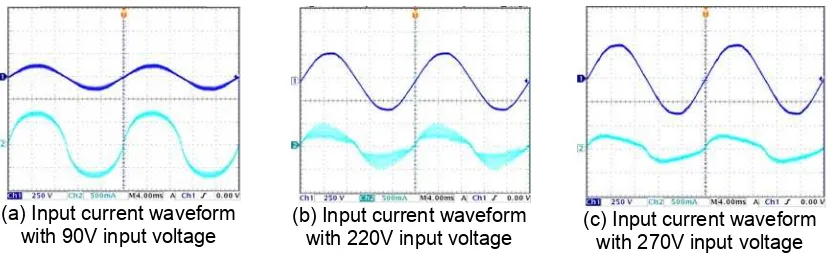
(a) Input current waveform with 90V input voltage
(b) Input current waveform
with 220V input voltage (c) Input current waveform with 270V input voltage
60 80 100 120 140 160 180 200 220 240 260 280 0.970
0.975 0.980 0.985 0.990 0.995 1.000
Input Voltage (V)
Power F
a
c
[image:5.595.196.399.82.236.2]tor
Figure 4.Relationship curve between input voltage and power factor
Figure 3. is the input current waveform measured with different input voltages (90 V, 220V and 270V) and the output loaded with 100 W. Clearly, the input current is close to the standard sinusoidal wave and the measured power factor is greater than 0.96. The relationship between the input voltage and the measured power factor is shown in Figure 4. It can be seen that the power factor decreases as the input voltage increases, but the value is always larger than 0.96. This is consistent with the conclusion from Equation (10), the lower the input voltage is, the smaller the coefficient k of the Equation (10) is, and then the closer the power factor is to 1.
60 80 100 120 140 160 180 200 220 240 260 280 86.5
87.0 87.5 88.0 88.5 89.0 89.5 90.0 90.5
Input Voltage (V)
Eff
iciency
[image:5.595.104.275.395.531.2](%)
Figure 5.Output current (1A/div, 4ms/div) Figure 6. Relationship curve between input voltage and efficiency
Figure 5 shows the output current waveform when the input voltage is 220V and the output is full-load. It can be seen that the output current is constant at 3.2 A, the ripple current peak is 150 mA, the output current ripple is 4.7%, and the output current is superimposed with the ripple current whose frequency is 2 times of the mains frequency (about 100HZ). Improving the working speed of the control loop and increasing the capacitance of the input capacitor can reduce the output ripple, but would reduce the power factor of the circuit. On the other hand, increasing the capacitance of the output capacitor (such as multiple capacitors in parallel) can also reduce the output ripple, but would increase the cost of the circuit. Therefore, it is necessary to balance the output ripple, the power factor and the cost when designing a circuit.
[image:5.595.313.499.396.532.2]4. Conclusion
A high power factor single-stage flyback converter for LED lighting application has been studied in this paper. The stability of the flyback topology operating in boundary conduction mode was analyzed in details. Based on these analyses, a prototype of 100W flyback LED driving power has been designed and tested. The experimental results show that the LED drive power supply with fewer components and lower dissipation can achieve power factor correction and constant current control of LED. When the input voltage is 220V, the power factor is greater than 0.97 and the conversion efficiency is more than 90%, thus it has great practical application values.
Acknowledgements
The work described in this paper is supported in part by the key industry problem plan of Shaanxi Province Industry Science and Technology under grant 2016GY-074.
References
[1] M Orabi, T Ninomiya. A unified design of single-stage and two-stage PFC converter. IEEE 34th Annual Power Electronics Specialist Conference (PESC '03). 2003; 4: 1720-1725.
[2] SY Chae, BC Hyun, P Agarwal, WS Kim, BH Cho. Digital Predictive Feed-Forward Controller for a
DC-DC Converter in Plasma Display Panel. Twenty Second Annual IEEE Applied Power Electronics
Conference (APEC 2007). 2007: 894-898.
[3] Mallisetti Rajesh Kumar, Duraisamy Lenine, Ch Sai Babu.
A variable switching frequency with boost power factor correction converter. TELKOMNIKA Telecommunication Computing Electronics and Control. 2011; 9(1): 47-54.
[4] M Derkaoui, A Hamid, T Lebey, R Melati. Design and modeling of an integrated micro-transformer in a flyback converter. TELKOMNIKA Telecommunication Computing Electronics and Control. 2013; 11(4): 669-682.
[5] L Yu-Kang, L Jing-Yuan, W Chao-Fu, L Chien-Yu. Analysis and design of a dual-mode flyback converter. 2010 IEEE International Conference on Sustainable Energy Technologies. 2010: 1-3. [6] Tzuen-Lih Chern, Li-Hsiang Liu, Su-Hong Yeh, Yu-Lun Chern, Der-Min Tsay. Single-stage flyback
converter for LED driver with inductor voltage detection power factor correction. 2010 5th IEEE
Conference on Industrial Electronics and Applicationsis. 2010: 2082-2087.
[7] Hao Ma, Yue Ji, Ye Xu. Design and Analysis of Single-Stage Power Factor Correction Converter With a Feedback Winding. IEEE Transactions on power electronics. 2010; 25(1): 1460-1470.
[8] Sang Cheol Moon, Gwan-Bon Koo, Gun-Woo Moon. An interleaved single-stage flyback AC-DC converter with wide output power range for outdoor LED lighting system. Applied Power Electronics Conference and Exposition (APEC), 2012 Twenty-Seventh Annual IEEE. 2012: 823-830.
[9] Sang Cheol Moon, Gwan-Bon Koo, Gun-Woo Moon. A New Control Method of Interleaved Single-Stage Flyback AC–DC Converter for Outdoor LED Lighting Systems. IEEE Transactions on Power Electronics. 2013; 28: 4051-4062.