Design of Gain Booster for Sample and Hold Stage
of High Speed-Low Power Pipelined
Analog-To-Digital Converter
Mohd Hafiz bin Jali
Faculty of Electrical Engineering Universiti Teknikal Malaysia Melaka(UTeM)Hang Tuah Jaya 76100 Durian Tunggal, Melaka
Malaysia
Abstract - This paper presents the full custom design of
an operational transconductance amplifier (OTA) for the sample and hold (SHA) stage of a 10-bit 50-MS/s pipelined analog-to-digital converter (ADC) implemented in a TSMC 0.35 m CMOS process. The OTA chosen for this design is folded cascode with gain boost topology. It is demonstrated through the design analysis and HSPICE simulation that such a structure realizes the best trade-off between power, speed and gain. The simulation results show the OTA achieves DC gain of 88.05dB, unity gain bandwidth of 430.03MHz and 84.06 degree of phase margin. The OTA achieves 62.13 dB SNR at the sampling rate of 50MHz with the input frequency of 24MHz. Power consumption is 9.68 mW from a single 3V supply. The settling time to 2-11 accuracy is 8.2ns.
Index Terms - Gain boost, folded cascode, sample and
hold amplifier, pipelined ADC.
I. INTRODUCTION
Speed and accuracy are two of the most important properties of analog circuits such as switch-capacitor filters, sigma-delta converters, sample and hold amplifier and pipeline ADC; however, designing high performance analog circuits is becoming increasing challenging with persistent trend towards reduced voltage supply. The main bottleneck in the analog circuit design is the operational amplifier. Speed and accuracy are determined by the settling behavior of operational amplifiers. Fast settling requires a high unity-gain frequency and a single-pole settling behavior of the op amp, whereas accurate settling requires a high dc gain. In a low voltage circuit, the realisation of the CMOS operational amplifier that combines high DC gain with high unity gain bandwidth has proven to be a difficult problem.
Cascading is a most useful technique to achieve DC requirement of the amplifier without degrading its high frequency performance. But cascading is not
possible in low voltage circuits owing to output voltage swing consideration. Gain-boosting technique was introduced to remedy this problem. It allows increasing the DC gain without sacrificing the output voltage swing. Furthermore this technique decouples the DC gain and the frequency response of the amplifier [2]. It is therefore possible to achieve high speed and high gain at the same time.
This paper is organized as follows. Section II describes the design methodology. Section III provides an overview of the gain boost techniques of a folded cascode amplifier. Section IV illustrates detailed circuit implementation of the OTA. Section V presents the specification of pipelined ADC. Section VI explains the design analysis of the OTA, biasing and common mode feedback circuit employ in the OTA. Section VII and VIII discuss about the SHA and Fast Fourier Transform (FFT). The simulation result and discussion from different process corner is comment on section IX. Section X shows the post layout simulation result. Conclusion is finally drawn in the last section.
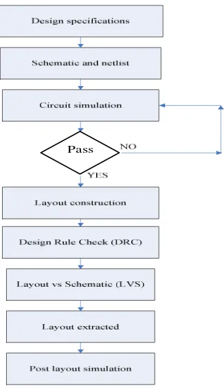
II. METHODOLOGY
Pass
Figure 1: Design flow
III. FOLDED CASCODE WITH GAIN BOOST TOPOLOGY
M2
0
I1
C1
0
C4
Vin
I2
M3
0 0
M1
C3 X
CL
C2
0 Y
Vout
Figure 2: Gain boosted folded cascode topology
The difficulties in using two-stage op-amps at high speeds have motivated extensive work on new topologies. Gain Boosted amplifiers are proposed instead of the normal folded cascode amplifiers to get both high gain and high bandwidth from a single stage amplifier. The idea of gain boosting is to maximize the output impedance without adding more cascode devices. It is usually widely used for high-impedance current source [1].
Figure 2 show the gain-boosted folded cascode topology where transistors M1 and M2 form the main folded amplifier (M1=Input device, M2=Cascode device). C1, C2, C3, and C4, are the parasitic capacitances between
drain to source and gate-to-source of different transistors. CL, is the load capacitance seen at the output node. The
gain obtainable from just these two transistors is limited (around 60 dB for a fully-telescopic amplifier) as the gain increase further, the parasitic poles becomes more dominant and hence the bandwidth starts dropping [3]. M3 (gain boost device) is put which creates a negative feedback loop that makes the source of M2less sensitive to the output voltage to overcome this problem [2] .M3 drives the gate of M2 and force VX to be equal to VY
.Thus, voltage variation at the drain of M2 now affect Vx to a lesser extent because the gain boost devices regulated the voltage [1].
The gain boost device with gain Add increase the
output resistance approximately Add times larger than that
of normal folded cascode amplifier [4]. Therefore gain boosting technique increased the output impedance and DC gain by the additional gain stage Add without adding
more cascode devices. From figure 1,with transconductance gm1,gm2 and output resistance rds1,rds2 of M1 and M2 respectively, the output resistance Rout and DC gain Adc of the gain boost cascode OTA is given by equation below [2] :-
Rout = gm2rds2rds1Aadd (1)
Adc = gm1gm1rds1rds2Aadd (2)
IV. CIRCUIT IMPLEMENTATION
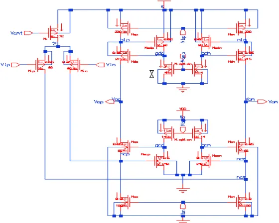
Figure 3 shows the fully differential folded cascode gain boost topology. The differential amplifier is choose over single-ended signaling because of higher immunity to environmental noise [1]. Now consider the circuit is symmetric, noise on VDD affects Vop and Vom but not the difference between these nodes. Thus the circuit is much more robust to the supply noise [1]. Another reason is to increase the maximum achievable output swing. The differential circuit produce double maximum output swing than that in the single ended circuit. Other reasons using differential circuits is simpler biasing and high linearity [1].
adds minimal power. Since the main function of the gain boost device is to increase the gain of the OTA, longer channel length are used to get larger output resistance.
Transistors in the signal path are biased in deep inversion instead of at edge of saturation to ensure that they remain in saturation at all process corners. For cascode transistors (Mcp, Mcm, Mdp, Mdm) minimum
channel lengths were chosen for both NMOS and PMOS in order to place the non-dominant pole of the OTA at high frequency.
The use of small device sizes reduces the parasitic capacitance seen at the output node, thus improving the OTA’s speed. This also minimizes capacitive load seen by the gain boost devices, which
Figure 3 : Fully differential folded cascode topology
results in lowering the power dissipation of the gain boost devices. For the PMOS current source and the NMOS current sink in the cascode device, longer channel lengths are used to obtain higher open loop gain and for better matching .
V. SPECIFICATION OF PIPELINED ADC
The method of designing a pipelined analog-to-digital converter for minimum power consumption has been described at the system level [5]. The front end of the converters has a sample and hold stage followed by eight 1.5-bit residue amplifiers and at the back end of the ADC is only 2-bit flash converter as shown in figure 4:-
Figure 4: 10-bits 50MS/s pipelined ADC architecture
The design goal is to meet the specification for the SHA stage of the pipelined ADC over all process corners while minimizing power. The specification is tabulated below:-
Table 1 ; Design specification
Parameters Specification
Stage Capacitor (Cf) 1.22pF
Load Capacitor (CL) 1.2pF
Settling Accuracy (ess) 2-11
Settling Error 0.1% Feedback Factor (ß) 0.9 Input Voltage Swing 1Vp-p
DC Gain (AVdc) >72dB
GainBandWidth (GBW) >350MHz Phase Margin (PM) >65o
Settling Time (ts) <9ns
Power Consumption <20mW
VI. DESIGN ANALYSIS
A. OTA
+
chosen as the smallest effective voltage that keeps the input transistors in the strong inversion region and satisfies the
Then the sizing of the input transistor is obtained using this equation:-
To obtain sizing of other transistors, use this equation:- optimization during simulation, the design parameters is summarize as table 2.
Table 2: Summary of design parameter
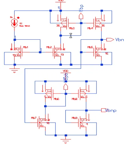
Devices W reasonable accuracy [1]. In order to maximize performance, a robust biasing circuit must be employed. A high-swing cascode current mirror is used to maximize robustness over process and supply voltage variation while also providing excellent current mirroring.
Figure 5 : Biasing Circuit
Table 3 shows the transistors sizing after optimizing during simulation to obtain a proper biasing current.
Table 3: Biasing device’s parameters.
C. Common-Mode Feedback
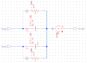
Figure 6: Common Mode Feedback circuit
Figure 6 is common mode feedback for the OTA. For the full differential signal circuitry, because of the increased symmetry, all common mode signals and even-order distortions cancel out, except for the influence of component mismatches. However, as the signal is no longer referred to ground, the operating point of the circuitry cannot be stabilized with the differential feedback loop. A common-mode feedback loop (CMFB) is required to determine the output common-mode voltage and to control it to be equal to some specified voltage. This voltage is feedback to control the current levels. Thus, both side carried larger currents and bring the common mode voltage of output nodes back to value Vcmt [8]. So, the common-mode feedback is needed to fix the voltages at the high impedance output nodes to the desired value.
VII. SAMPLE AND HOLE AMPLIFIER (SHA)
cmiop
+
-+
-Cl+ Vin+
phi1 phi1
in-phi2 fn
fp
0
phi2
phi1a
cfn
out+
Vin-in+
phi1a
out-cfp
0
phi1a
Cl-Figure 7: Sample & hold stage of a pipelined ADC
Sample-and-hold amplifier circuits are key building blocks for many discrete time signal processing applications including pipeline A/D converters. Its basic function is to transform input continuous signals into discrete time signals and amplify them. Using the techniques of precharging and output capacitor coupling can mitigate the requirements for the opamp, resulting in low power dissipation The conventional flip-around SHA shown in Fig. 7 has been extensively employed for high-speed and high-resolution CMOS SHA. When phi1 = 1, the
SHA is in the sample mode, and the input is sampled on the
Cfp and Cfn capacitors. When phi2 = 1, the SHA is in the hold mode, the sampling capacitors are connected to the outputs of the op-amp. The op-amp and the two sampling capacitors form a feedback loop to drive the Cl- and Cl+
capacitive loads [6].
VIII. FAST FOURIER TRANSFORM (FFT)
Figure 8 : FFT spectrum
The simulation results from HSPICE are post processed by the software of MATLAB to obtain the Fast Fourier Transform (FFT) spectrum. FFT is used as a tool for measuring and analyzing signals from captured data records. It captured time-domain signals, measure their frequency content, convert the results to convenient units, and display them. FFT produced the average of a signal’s frequency content over the time interval that the signal was acquired. FFT focus on the positive half of the frequency spectrum only, noting that the spectrum of a real signal is symmetrical. In a two-sided spectrum, half the energy resides in the positive frequencies and half in the negative frequencies. Therefore, to convert from a two-sided spectrum to a single-sided spectrum, the second half of the matrix is discarded and multiplies every point by two.
IX. SIMULATION RESULT AND DISCUSSION
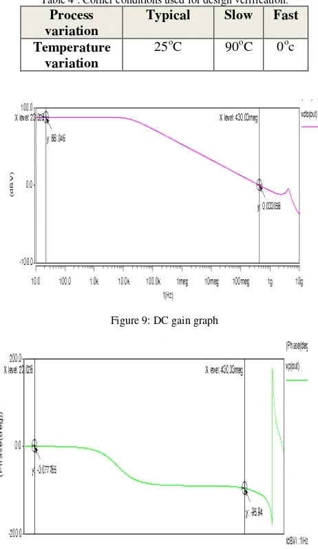
The following process corner conditions are used in verification of the OTA design. Usually for commercially product, temperatures varies from 0oC to 90oC, these are combined with process variations to derive worst case scenario. For example, highest temperature gives rise to the highest thermal noise figure. Combined with the slow process parameters. It places the toughest test on the dynamic range performance. On the contrary, the fast process corner combined with low temperature will probably introduce instability problem.
Table 4 : Corner conditions used for design verification.
Process variation
Typical Slow Fast Temperature
variation
25oC 90oC 0oc
Figure 9: DC gain graph
Figure 10: Phase margin graph
The OTA has a DC gain of 88.05dB as seen in figure 9 while the unity gain bandwidth reaches 430.03MHz with an approximate 84.06 phase margin in figure 10.It shows the effect of gain boosting technique; the OTA exhibit a high DC gain measurements without affecting the gain or phase for higher frequencies.
Figure 11: Transient response graph
Figure 12: Settling time
Figure 11 show the transient response of the OTA to see the settling behaviour. Settling time is the time elapsed from the application of an ideal instantaneous step input to the time at which the amplifier output has entered and remained within a specified error, usually symmetrical about the final value. To see the result, the OTA must be placed in a closed loop configuration. The setup to be used in the SHA stage of a 10-bit 50-Ms/s pipelined ADC is shown in Figure 7. From the figure, phi1 and phi2 are non overlapping clocks, Cfp, Cfn are both the sampling and feedback capacitors depending on which clock phase the circuit operates. From figure 12, the settling time of the OTA is 8.2ns which is faster than the expected result that is 9ns. It is predictable result since gain boosting technique decouples the DC gain and frequency response. Therefore a high speed and gain is possible to achieve at the same time.
Table 5 summarizes the achieved performance of the design. The specifications are met throughout the corner conditions.
Table 5 : Performance summary
Process Corner Worst ,90oC
Typical ,25oC
Best ,0oC
DC Gain (dB) 87.16 88.05 88.12 Gain BandWidth
(MHz)
367.47 430.03 477.55
Phase Margin (degree)
83.68 84.06 84.46
Settling Time (ns) 8.43 8.2 8.16 Power
Consumption (mW)
9.65 9.68 9.82
SNR (dB) 57.78 62.13 69.08
Voltage (V) 3 3 3
X. POST LAYOUT SIMULATION
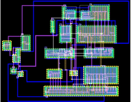
Figure 13 : Op-amp layout
Figure 13 is the layout of the op-amp. The layout is generated by performing Schematic Driven Layout (SDL) in IC station Mentor-Graphic using TSMC 0.35 m CMOS process in the Mentor-Graphic environment. The performance of a full-custom design can be best analyzed by performing a post-layout simulation on the extracted circuit netlist. The parasitic capacitances extracted according to how the layout is designed. At this point the circuit should have passed the DRC and LVS steps with no violations.
The post layout simulation is performed by obtaining the netlist of the layout design from Mentor-Graphic and run it in HSPICE. There are subtle differences in the post-layout simulation results as compared to the pre-layout simulation as shown in Table 6 but it is acceptable since it is still within the specifications.
Table 6 : Pre and post-layout performance
Performance Pre-layout Post-layout
DC Gain (dB) 87.25 87.25
GainBandWidth (MHz) 418.9 408.08 Phase Margin (degree) 79.9 79.74
Settling Time (ns) 8.27 8.162 Power Consumption (mW) 9.59 9.59
SNR(dB) 54.61 51.02
XI. CONCLUSION
This paper presents the full custom design of an operational transconductance amplifier (OTA) implemented in a 0.35 m CMOS process using HSPICE. The choosen OTA is a single stage folded cascode with gain booster to fulfill the high DC gain and unity gain bandwidth requirement. All the design specs have been verified throughout the process corners and temperature variations and has satisfied all the specifications given in advance. The HSPICE simulation results show the OTA achieves DC gain of 88.05dB, unity gain bandwidth of 430.03MHz and 84.06 degree of phase margin. From the MATLAB simulation, the OTA achieves 62.13 dB at the sampling rate of 50MHz with the input frequency of 24MHz. Power consumption is 9.68 mW from a single 3V supply. The settling time to 2-11 accuracy is 8.2ns. The low power, low voltage, high speed result has been successfully achieved for both the performance and robustness. It is concluded that this architecture is suitable for low power-high speed pipeline ADC.
FUTURE DEVELOPMENT
The design of the OTA can be further analyze by considering other performance specifications and also implemented it in a low-power low-voltage technology such as TSMC 0.18 m but needs major modification in order to work in lower supply voltage.
ACKNOWLEDGMENTS
The author would like to thanks Universiti Teknikal Malaysia Melaka(UTeM) for their support in completing this project.
REFERENCES
[1] Behzad Razavi, “Design of Analog CMOS Integrated Circuits” 2001.
[2] K. Bult and G. Geelen, “A fast-settling CMOS op amp for SC circuits with 90-dB gain,” IEEE J. Solid State Circuits, Vol. 25, Dec. 1990, pp. 1379–1384.
[4] E. Sackinger and W. Guggenbuhl, “A high swing high impedance MOS cascode circuit,” IEEE J. Solid State Circuits, Vol. 25, Feb. 1990, pp. 289–298.
[5] Reza Lofti, Mohd. Taherzadeh Sani, M. Yaser Azizi and Omid Shoaei, “Systematic Design for Power Minimization of Pipelined Analog-to-Digital Converters” IEEE Intl. Conf. on Computer Aided Design ICCAD 2003.
[6] Cheng-Chung Hsu and Jieh-Tsorng Wu,”A 33-mW 12-Bit 100-MHz Sample-and-Hold Amplifier”, Department of Electronics Engineering, National Chiao-Tung University, Hsin-Chu 300, Taiwan. [7] Paul C. Yu, “A 2.5-V, 12-b, 5-msample/s Pipelined CMOS ADC”. Member, IEEE, and Hae-Seung Lee, Fellow, IEEE, IEEE Journal of Solid-state
Circuits, vol. 31, no. 12, December 1996.
[8] T. Danelle Au and Kelvin Khoo, “A 13-Bit, High- Gain, 3V CMOS Differential Transconductance Amplifier” University of California at Berkeley Department of Electrical Engineering and Computer Sciences.
[9] Yamu Hu “CMOS Low Voltage Preamplifier Based on 1/F Noise Cancellation” Departement de Genie Electrique et de Genie Informatique Ecole
Polytechnique de Montreal Memoire Presente en Vue de L’obtention Du Diplome de Maitrise es Science Appliquees (Genie Electrique .)
[10] Paul C. Yu, “5-msample/s Pipelined CMOS ADC”, IEEE Journal of Solid-state Circuits,
