Effect of Two Different Superstrate Layers
On Bismuth Titanate (BiT) Array Antennas
F. H. Wee1, F. Malek2, A. U. Al-Amani3& Farid Ghani11School of Computer and Communication Engineering, Universiti Malaysia Perlis, Perlis, Malaysia,2School of Electrical Systems
Engineering, Universiti Malaysia Perlis, Perlis, Malaysia,3School of Materials and Mineral Resources Engineering, Universiti Sains
Malaysia, Malaysia.
The microwave industry has shown increasing interest in electronic ceramic material (ECM) due to its advantages, such as light weight, low cost, low loss, and high dielectric strength. In this paper, simple antennas covered by superstrate layers for 2.30 GHz to 2.50 GHz are proposed. The antennas are compact and have the capability of producing high performance in terms of gain, directivity, and radiation efficiency. Bismuth titanate with high dielectric constant of 21, was utilized as the ECM, while the superstrate layers chosen included a split ring resonator and dielectric material. The superstrate layers were designed for some improvement in the performance of directivity, gain, and return loss. The proposed antennas were simulated and fabricated. The results obtained were small antennas that possess high gain and high directivity with 360
6
, omni-directional signal transmission that resonant types of conventional dipole antenna cannot achieve. The gain of the antenna with the superstrate layer was enhanced by about 1 dBi over the antenna without a superstrate layer at 2.40 GHz.E
lectronic ceramic material (ECM) has some interesting characteristics, such as small size, ease of fabrica-tion, high radiation efficiency, large impedance width, and low production cost1. An ECM antenna can be made much smaller than conventional metal antennas. Quan et al.2worked on broadband, omnidirectional antennas with bandwidths of 800 MHz, which was wide enough to cover the frequency bands up to 2.4 GHz. The antenna was an array antenna that had 3.8 cm of electrical size with a gain of 4.5 dBi. Hence, this analysis triggered our interest in studying the properties of BiT ECM for potential application on the antenna for the production of miniature, omnidirectional antennas with higher gain, allowing microwave communications that demand the miniaturization of microwave circuits. The characteristics of ECMs make them a better choice for antennas than the conventional, low-gain elements, such as dipoles, monopoles, and microstrip patches3. ECM also offers many benefits when used in an antenna because it has no metallic loss and offers high radiation efficiency through millimeter-wave and microwave frequencies4–6.Palukuru et al.7also developed a rectangular-shaped, dielectric resonator antenna. But they used a barium strontium titanate-cylic olefin copolymer (BST-COC) composite dielectric material in an antenna for 2.4 GHz applications. The BST-COC DRA is a very compact antenna that measures 19 mm310 mm35 mm and covers 2.4 GHz WLAN applications. However, the research related to the BST-COC antenna was not concern about the performance of the antenna for cases in which the peak gain and radiation efficiency only met the minimum standard gain and radiation efficiency values of a dipole antenna, i.e., 4 dBi and45%. These poor results occurred due to the low dielectric constant and the high utilization of metal on the antenna due to its copper foil shape and microstrip feed line. The proposed antenna was composed of more than 90% dielectric material, which covered the transmission line. This can be attributed to the relatively weaker surface currents on the ground plane of DRA in order to achieve high radiation efficiency. Also, an ECM antenna features mechanical simplicity, simple coupling schemes to all commonly-used transmission lines, and ease of excitation. An ECM antenna can use different feed mechanisms, such as probes, microstrip lines, slots, and co-planar lines. An ECM antenna also is more resistant to proximity detuning when it is placed adjacent to, or in the vicinity of, another object.
Microstrip antennas possess major shortcomings, such as narrow impedance bandwidth and low efficiency and gain, which seriously limit their application. Additional research was conducted by Aras et al.8on the dielectric resonator antenna (DRA) using a disk shape. They claimed that the DRA consisted of high dielectric constant materials and was mounted on a dielectric substrate that had lower permittivity. But the authors also claimed that the dielectric material had a high quality factor (Q-factor) that led to a narrower bandwidth of 140 MHz at the resonant frequency of 2.415 GHz. The unloaded Q-factor of the proposed antenna was measured at the low Q-factor of 40.2, which is suitable for use in obtaining wider bandwidth. Many broadband techniques
SUBJECT AREAS:
ELECTRICAL AND ELECTRONIC ENGINEERING
ELECTRONIC DEVICES
Received 25 July 2013
Accepted 11 December 2013
Published 15 January 2014
for microstrip antennas have been reported9,10, and to overcome the disadvantage of low gain, some papers has proposed gain enhance-ment methods using multiple superstrates11,12.
The design that was proposed in this study consisted of a rect-angular-shaped ECM array antenna with superstrate layers attached. However, the presence of superstrate layers above an antenna may adversely affect the antenna’s basic performance characteristics, such as gain, radiation resistance, and efficiency. For this reason, it is important to analyze superstrate effects so adequate superstrate para-meters can be chosen to enhance gain and radiation efficiency. It has been reported that higher gain can be achieved if the substrate and superstrate layers are used appropriately11. In this study, bismuth titanate (BiT) and a superstrate layer were of considerable interest for a range of applications, including microwave antennas and filters, due to their high dielectric constant and low conduction loss1–6. This paper compares the gain of a single patch with superstrate layers with that of a single patch without superstrate layers and reports the experimental results for 6-element, BiT, array antennas with and without a superstrate layer. The details of the proposed antenna design and results are presented in the following sections.
Results
Electronic ceramic material sample.A bismuth titanate solution was prepared by slowly adding the titanium solution to the prepared bismuth solution to obtain a precursor solution. The precursor solution was stirred continuously and then heated to 80uC to form a sticky gel, which was combusted to produce as-combusted powder. The details are described in13. Prior to the ECM application, we investigated the crystal structure and surface morphology of the bismuth titanate as in13. Based on Scanning Electron Micrograph (SEM), it was apparent that the particles in the bismuth titanate were very dense, free of cracks, and had a few small pores at the grain boundaries and junctions. This agrees with its relative density of about 98% that had been determined in earlier tests. The X-ray diffraction (XRD) pattern of the sintered BiT observed indicated that very high purity BiT was created and that preferential orientation was obtained14. We also investigated the dielectric properties of BiT in13. The tests showed that the BiT exhibited low losses because it is a free conducting material that has no current flowing on its surface.
Superstrate layers. A split ring resonator (SRR) is one of the elements from metamaterial, which is an artificial media characterized by constitutive parameters generally not found in nature whose values can be engineered to specified values15. SRR that exhibits unique properties that do not exist in natural materials has attracted great interest in the last few years15–17. SRR is also called left-handed material (LHM), in which the vectorsE,H, and k form a left-handed system. The SRR exhibited negative permittivity and permeability for which several names and terminologies have been suggested, such as ‘‘left handed’’ media or double-negative (DNG) metamaterials. Since the idea was proposed by Victor Veselago in 196817, the availability of such a material has been accepted and extended.
Recently, the demand for planar high directivity antennas, which can be applied to high-speed wireless LAN, satellite reception, and various point-to-point radio links, has increased significantly. In the past few years, new methods for improving the antenna gain have been developed, and the SRR has been proposed18,19and theoretically discussed19. In those works, various metallic structures were used as SRR to achieve certain unusual characteristics, which are suitable for high-gain and high-directivity designs.
For a microstrip transmission line of width, w, and a conventional microwave substrate height, h, one has the approximate result for the effective relative permittivity of the air-substrate-microstrip system20:
With F1561(2p26)exp[230.666 h/w]0.7528], and the electrostatic relative permittivity is20:
With
The goal is to design a length of SRR-loaded transmission line that can be included in some manner with the same length of microstri-pline to make the paired system dispersionless; that is, we want to produce a dispersion-compensated segment of transmission line. This means we want to introduce a metamaterial with relative per-mittivityeMTMand permeabilitymMTMso that the overall relative permittivity and permeability of the system are20:
eð Þf
e0 ~eeffð Þf zeMTMð Þf ;
mð Þf
m0 ~1zmMTMð Þf ð6Þ
in such a manner that the wave impedance in the metamaterial remains the same as it is in the original substrate, i.e.20:
Z~
And the index of refraction in the medium compensates for the dispersion effects associated with the microstrip geometry itself; that is the effective index of the pair becomes that of free space20:
neffð Þf ~
These conditions are satisfied if
eeffð Þf ½1zmMTMð Þf ~eMTMð Þf zeeffð Þf ð9Þ
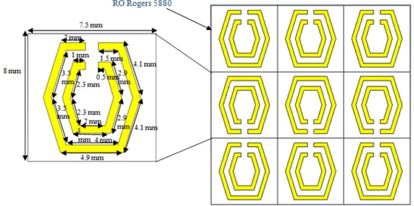
structure are shown in Fig. 1(a). Nine unit cells of SRR with the same hexagonal structure were combined into a slab to develop a split ring resonator cover. The constructed slab is shown in Fig. 1(b). The constructed slab was located at a distance, d, from the conventional antenna to act as a cover. The distance, d, can be varied to obtain the best return loss and radiation pattern. The combination of the SRR slab and the BiT array antenna will be further discussed in ECM Array Antenna with Superstrate Layers section.
Another method was chosen in order to obtain high gain and directivity of this antenna, i.e., a dielectric layer with appropriate thickness and loss tangent. The thin dielectric layer that helps to reduce weight also was able to reduce the surface wave losses. The dielectric layer’s dielectric constant,e9, has an important role similar to that of the thickness of the dielectric layer. A low value ofe9for the dielectric layer will increase the fringing field of the patch and thus increase the radiated power21. A large gain can be obtained for radi-ation at any desired angle in the form of a pencil beam at broadside or a conical beam pointing at an angle,h22. The dielectric layer will act as an optimum reflecting surface when the thickness is chosen so that it is an odd multiple of one quarter of a wavelength in the vertical direction. This corresponds to the condition22:
t~ 2m
where m is a positive integer, and n2is the refractive index of the dielectric layer. Using m51, gives the thinnest dielectric layer.
The resonant frequency results from the relationship between the speed of light in a material and the dielectric permittivity are shown in equation 1223:
Thus, as the relative permittivity is increased, the speed of light in a material decreases. For a resonant structure, this slower speed means an object loaded with the dielectric materials ofer.1 will have a lower resonant frequency than an unloaded, identical-size structure. Therefore, these loaded structures are said to be ‘‘electrically larger’’ than their unloaded counterparts of the same physical size.
The resonant frequency of the dielectric layer can be calculated from equations (13)–(16)23. Equation (13) represents an effective
relative permittivityereff, which is a modified relative permittivity value that accounts for the fields fringing in the air above the sub-strate material23.
Then, this modified relative permittivity value is used to find the length extensionDL that accounts for the fringing fields at the each of the radiating edges23.
DL~h0:412 ereffz0:3
The effective length Leff, can be calculated using the results of equa-tion (15)23:
Leff~Lz2DL ð15Þ
This allows the resonant frequency to be calculated using the new effective length, as shown in equation (16)23:
fr~
The resonant frequency and the permittivity are inversely related, such that increasing the permittivity decreases the resonant fre-quency of the antenna. This allows the production of a simple, sig-nificantly miniaturized antenna without adding complexity to the metal patch, such as a slot or a slit for the wideband antenna or the large array patches used by larger antennas for higher gain. Since a simple ECM can be etched onto a high permittivity substrate to achieve a smaller size for a given operating frequency without modi-fying its shape, this can be beneficial for manufacturing and for mechanical robustness.
A low-loss tangent reduces the dielectric loss and therefore increases the efficiency of the antenna22. Thus, the parameters of the dielectric layer so chosen are Tarconic CER-10, with a thickness of 0.5 mm, permittivity ofe95 10, and a loss tangent, tand 5 0.000422. The optimum sizes obtained were 2032530.5 mm, as shown in Fig. 2, with the length of the dielectric layer being shorter
Figure 1| SRR (a) Dimensions of the single unit cell construction using split ring structures; (b) A SRR slab from a combination of nine unit cells. The HSRR layer consists of 333 units, so the size of the substrate and the cover is 22.5mm324mm. The width and the split distances of HSRR are
than the length of the HSRR layer. This condition is to make sure the resonant frequency is 2.4 GHz, according to the equation (16). The details on the combination of dielectric layer and BiT array antenna will be discussed in ECM Array Antenna with Superstrate Layers section.
ECM array antenna.The frequency behavior of the ECM antenna suggests that the antenna supports both the WLAN and WiMAX
ranges. In designing an ECM array antenna, one also must consider the possibility of the high loss associated with the antenna. Numerical simulation shows high levels of conduction loss and power loss with the utilization a metallic structure for an antenna. Therefore, ECM array antennas were designed with low loss BiT elements that present negligible metallic loss in the structure of the antenna, thereby reducing the loss factor that will lead to low performance of the antenna13. One of the principle shortcomings is that a microstrip array antenna with a feed network exhibits a relatively large insertion loss, especially when the array is high in surface current or when it is operating at higher frequencies. At microwave frequencies, the loss in copper transmission lines becomes significant. Thus, it is crucially important to minimize insertion loss when designing the power division transmission lines. A series-feed, linear array results in a more compact, lower-loss network that requires less transmission line lengths and fewer junctions that parallel-feed arrays. This results in a lower insertion loss than the parallel feed13.
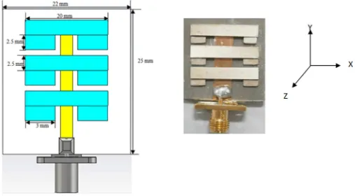
The design for the series-fed, linear, ECM-array antenna was based on a resonant-array approach, in which a standing wave was assumed on the microstrip antenna. This assumption led to a fairly good prediction of the miniaturization of the array when the number of ECM elements is less and the amount of coupling from the micro-strip line for each ECM array element is relatively low. For greater numbers of ECM elements, the coupling to each element is greater. Thus, for the proposed ECM array antenna that is designed in array form and has a smaller size, the standing wave also is to be presented in each of the ECMs, leading to high coupling with better perform-ance of the antenna. The layout structure of the six-element, BiT array antenna is shown in Fig. 3. The height, h, of the antenna was 25 mm. The antenna was composed basically of four parts, i.e., three branching strips, six radiating patches, microstrip transmission lines, and the feed line. Those four parts were attached to the opposite sides Figure 2|Dimensions of the dielectric layer.Roger substrate board, RO
3010 was used as the dielectric layer that covered the six elements BiT array antenna. It comprisese9510.2 (dielectric constant) with size of 2032530.5 mm.
of a Rogers substrate board, RO Duroid 5880 substrate with dielectric constant, e9, of 2.2 and a thickness, t, of 1.6 mm. The parameters of the BiT array antenna were taken from13.
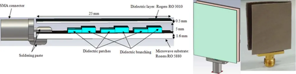
ECM array antenna with superstrate layers.Superstrate layers with dimensions of 2532030.5 mm and 24322.531.6 mm for dielectric layer and SRR layer, respectively, were placed above the radiating patch BiT elements at a distance of d55 mm22as shown in Fig. 4 and Fig. 5 respectively. The distance of 5 mm between superstrate layer with BiT antenna patch is the optimum distance at which to obtain high gain and high directivity. In this section, we describe our experimental investigation of the effect of a dielectric layer and SRR layer as the superstrate layer for high gain and high directivity on the six elements of the BiT array antenna, and we present the comparison between BiT array antenna with and without the superstrate layer.
The dielectric layer used was Rogers RO 3010 material due to its ability in reducing the surface losses, thereby leading to high radi-ation performance. The combinradi-ation of RO 5880 and the hexagonal structure made of perfect electric conductor (PEC) was used to build up the HSRR substrate. The PEC is very important for assuming the ideal case during the simulation to obtain the best results from the SRR. The detailed features are shown in Table 1.
The performance of the simulated BiT array antennas with the superstrate layers was analyzed using Computer Simulation Technology (CST) Microwave Studio, while the fabricated BiT array antenna with and without the superstrate layers were tested using performance network analyzer (PNA) and near-field test facility that available in university’s laboratory.
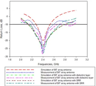
Fig. 6 shows a graph of return loss with the stacked of the super-strate layers on BiT array antennas. The simulated and measured
return losses obtained were functions of the frequency. Here, the frequency bandwidth of the antenna was defined as a return loss less than 10 dB. For the results of BiT array antenna with dielectric layer, the return loss was reduced to a highest value of 24.5 dB and 27.5 dB for the simulation and measurement results, respectively, as com-pared with the antenna without dielectric layer, which was 20 dB and 23 dB, respectively. This condition showed that the capacitive effects of placing the dielectric over the antenna did not affect the antenna’s performance.
From the results of the BiT array antenna with SRR layer, the return loss seems to have a similar reflectivity effect, which both antennas own the best transmission of signal compared to six-ele-ment BiT array antenna without superstrate layer. However, these results did not affect the overall performances of the BiT array anten-nas with and without the superstrate layer because their impedance matching was acceptable with more than 90% match.
The operating bandwidths of the proposed, six-element, BiT array antennas with and without the superstrate layers were found to be about 600 MHz for the two superstrate layers and 200 MHz without superstrate layer, respectively, which is compatible with the spe-cification of the WLAN and WiMAX systems. Overall, good agree-ments were found between the simulation and measurement results, although there was a slight discrepancy between them, which was believed to be due to to the environmental effect and mechanical tolerance, which were neglected in our simulations.
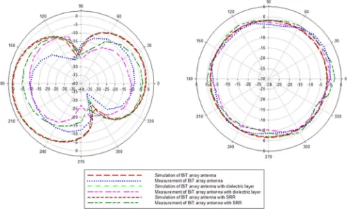
Fig. 7 shows the radiation pattern of a six-element, BiT, array antenna and a six-element, BiT, array antenna with superstrate layers in 2D view, which was analyzed in the vertical plane (XZ, YZ) and in the horizontal plane (XY) at 2.40 GHz. It can be observed that the 2-D radiation pattern of the co-polarization has a null ath590u. The
mode characteristics can be illustrated further by its 3-D patterns. Figure 4|Photograph of BiT array antennas with dielectric layer (a) simulated (b) fabricated.The antennas are composed of the radiating element and the dielectric layer withe9510.2 and thickness d50.5 mm (0.004l
gat 2.4 GHz). The superstrate is placed above the radiating patch at a distance 5 mm (0.04l0at 2.4 GHz), wherel0is the wavelength in free space, andlgis the wavelength in the medium of the superstrate (e510.2).
The beam peak is directional ath50u, radiating from the center of
the patch. Since the ground plane is finite, there is some back radiation that can be characterized by the front-to-back ratio, as mentioned earlier. The pattern resembles a donut shape in which the maximum direction of radiation is at an elevation angle ofh5
15ufrom the z-axis. These antennas provided a 360-degree coverage signal, which is in all directions (horizontally) for two-way commun-ication. The main directivity was directed at the vertical plane, which formed an omni-directional signal level in the H-plane. The H-plane has an important role because this parameter determines the point of strongest signal, thus avoiding signal redundancy and interference with other antennas radiating at the same plane. In this case, along E-field in Fig. 7(a), which correspond to the radiation directly overhead from the antenna, there is little power transmitted from the six-element, BiT, array antenna as compared to the six-six-element, BiT, array antenna without superstrate layers. The highest radiation intensity was provided by the six-element, BiT, array antenna with SRR layer. This was because this antenna exhibited the highest gain and directivity, which helped enhance the power signal of the antenna.
From Table 2, the gain of the six-element, BiT, array antenna, in radiation patterns, with dielectric layer and SRR layer exhibited 8.15 and 8.37 dB of gain and 8.53 and 8.66 dBi of directivity, respectively. The results show that the gain of the superstrate layers stacked on the six-element, BiT, array antenna was improved greatly compared to the common antenna. After studying both antennas, the overall results proved that the BiT array antenna with superstrate layers had better performances than the antenna that was designed without the superstrate layer.
Discussion
In the research reported in this paper, we introduced experimentally the effect of a superstrate layer for high gain on a electronic ceramic-material antenna. The radiating element with broadband and high radiation efficiency was designed to enhance the narrow bandwidth characteristic by a superstrate with high permittivity. We conducted experiments designed to compare the gain of a six-element, BiT array antenna with a superstrate to that of a six-element, BiT, array antenna without a superstrate layer. The six-element array antenna using superstrate layers had a high gain that exceeded 1 dBi and a wide impedance bandwidth of over 67%. Overall, the six-element, BiT, array antenna with HSRR had the best performance, followed by six-element, BiT, array antenna with dielectric layer, and, finally, the six-element, BiT, array antenna without the superstrate layer. The proposed antenna presented here will be useful for high gain systems that require a broadband bandwidth and will enable them to transmit and receive maximum signals.
Methods
The six elements of BiT antenna was simulated and fabricated for real application use, the size of the antenna with BiT element loaded was miniaturized. The most popular technique for reducing the size of a printed antenna is the use of a high- dielectric material for the radiating part. In doing so, the guided wavelength underneath the patch can be reduced and hence the size of the resonating patch also can be reduced.
Table 1 | Properties of Rogers RO 3010 and Rogers RO 5880 microwave substrate
Properties
Values
Rogers RO 3010 Rogers RO 5880
Permittivity,e9 10.2 2.2
Loss Tangent, tand 0.0004 0.025
Permeability,m 1 1
Thickness of the substrate, t 0.5 mm 1.6 mm
Figure 6|Comparison of return loss of the simulated and measured BiT array antennas and the BiT array antenna with the superstrate layer.
The reduction ratio is approximately related to the square root ofe924. Existing patch
antenna using ane0values in the range of 1 to 10 have a dimension of about 0.44l25.
However, for the BiT antenna using an e9value of 21, the size of the patch is reduced to about 0.20l. To further reduce the size, array elements of BiT materials were introduced. Depending on the number of BiT elements added to the patch antenna, a size reduction of about 28% can be achieved.
Conclusion
At the present time, antenna miniaturization is of great concern due to the physical benefits, and the design of the dielectric-resonator, ceramic antenna satisfies this need. Even though the proposed design is subject to the same adverse effects as other antennas, i.e., sag in the pattern shape, reduction of hardware measurement bandwidth, and return loss, it is sufficiently compact and has the proper impedance bandwidth for use in the range of 2.3 GHz to 2.5 GHz. Ultimately, BiT array antennas with superstrate layers were tested experimentally to enhance their multiple advantages for use in wireless antenna sys-tems. Compared to available microstrip patch antennas, these advan-tages include smaller size, higher radiation coefficient properties, wider bandwidths, and high gain and directivity for far distant radi-ation power. Eventually, our goal relative to BiT array antennas with
superstrate layers is to provide highly-efficient, miniaturized antennas with large bandwidths, low profiles, and low production costs. Such antennas are certain to be more efficient and effective than the con-ventional microstrip antennas for modern wireless systems.
1. O’Connor, E. M. & Long, S. A. The History of the Development of the Dielectric Resonator Antenna.ICEAA International Conference on Electromagnetics in Advanced Applications, Turin, Italy, 872–875, (2007), September 17–21. 2. Quan, X. L., Li, R. L. & Tentzeris, M. M. A broadband omnidirectional circulary
polarized antenna.IEEE Trans. Antennas. and Propag.61, 2363–2370 (2013). 3. Abdel-Wahab, W. M., Busuioc, D. & Safavi-Naeini, S. Modeling and design of
millimeter wave high Q factor parallel feeding scheme for dielectric resonator antenna arrays.IEEE Trans. Antennas. and Propag.59, 2834–2843 (2011). 4. Al-Zoubi, A. S., Kishk, A. A. & Glisson, A. W. Analysis and design of a rectangular
dielectric resonator antenna fed by dielectric image line through narrow slots.
Prog Electromagn Res.77, 379–390 (2007).
5. Ain, M. F.et al. 2.5 GHz BaTIO3dielectric resonator antenna.Prog Electromagn Res.76, 201–210 (2007).
6. Long, S. A., McAllister, M. W. & Shen, L. C. The resonant cylindrical dielectric cavity antenna.IEEE Trans. Antennas. and Propag31, 406–421 (1983). 7. Palukuru, V. K., Sonoda, K., Surendran, R. & Jantunen, H. BST COC composite
based rectangular dielectric resonator antenna (DRA) for 2.4 WLAN wrist applications.Prog Electromagn Res C.16, 195–205 (2010).
8. Aras, M. S. M., Rahim, M. K. A., Asrokin, A. & Aziz, M. Z. A. A. Dielectric resonator antenna (DRA) for wireless application, RF and Microwave Conference RMC2008, 454–458 (2008).
9. Sabban, A. A new broadband stacked two-layer microstrip antenna.IEEE AP-S Int. Symp. Digest.21, 63–66 (1983).
10. Jang, Y. W. Wide-band t-shaped microstrip-fed twin-slot array antenna.ETRI J.
23, 33–38 (2001).
11. Jackson, D. R. & Alexopoulos, N. G. Gain enhancement methods for printed circuit antennas.IEEE Trans. Antennas. and Propag,33, 976–987 (1985). 12. Yang, H. Y. & Alexopoulos, N. G. Gain enhancement methods for printed circuit
antennas through multiple superstrates.IEEE Trans. Antennas. and Propag35, 860–863 (1987).
13. Wee, F. H., Malek, F., Ghani, F. & Al-Amani, A. U. Integration of miniaturized array antenna with high-permittivity rectangular bismuth titanate for WiMAX applications.IEEE Trans. Antennas. and Propag.60, 6032–6036 (2012).
Figure 7|Radiation pattern in 2-D view (a) E-Field (b) H-Field.Both simulated and measured radiation pattern of the BiT array antenna with and without the dielectric layer are displayed in this figure.
Table 2 | Gain, Directivity, and Radiation Efficiency of BiT Array Antennas
Parameters (2.4 GHz)
BiT array anatenna without superstrate
layer
BiT array antenna with dielectric layer
BiT array antenna with SRR
Gain (dB) 7.02 8.15 8.37
Directivity (dBi) 7.42 8.53 8.66
Radiation Efficiency (%)
14. Sreekantan, S., Noor, A. F. M., Ahmad, Z. A., Othman, R. & West, A. Structural and electrical characteristics of crystalline barium titanate synthesized by low temperature aqueous method.J. Mater. Process. Technol.195, 171–177 (2008). 15. Smith, D. R., Padilla, W. J., Vier, D. C., Nemat-Nasser, S. C. & Schultz, S.
Composite medium with simultaneously negative permeability and permittivity.
Phys. Rev. Lett.84, 4184–4187 (2000).
16. Shelby, R. A., Smith, D. R. & Shultz, S. Experimental verification of a negative index of refraction.Science.292, 77–79 (2001).
17. Veselago, V. G. The electrodynamics of substances with simultaneously negative values ofeandm.Soviet Phys. Uspekhi.10, 509–514 (1968).
18. Chen, L., He, S. & Shen, L. Finite-size effects of a left-hand material slab on the image quality.Phys. Rev. Lett.92, 1–4 (2004).
19. Islam, M. T., Shakib, M. N. & Misran, N. High gain microstrip patch antenna.Eur. J. Sci. Res.32, 187–193 (2009).
20. Wiley-Interscience. Metamaterials physics and engineering explorations. [Engheta, N. & Ziolkowski, R. W.] [1–438], (Wiley-IEEE Press, August 2006). 21. Wee, F. H., Malek, F., Ghani, F., Sreekantan, S. & Al-Amani, A. U. High gain and
high directive of antenna arrays utilizing dielectric layer on bismuth titanate (BiT) ceramics.IEEE Trans. Antennas. and Propag1–8 (2012).
22. Li, B. & Kwok, W. L. Strip-fed rectangular dielectric resonator antennas with/ without a parasitic patch.IEEE Trans. Antennas. and Propag.53, 2200–2207 (2011).
23. 2ndedition Antenna Theory Antenna Analysis & Design. [C.A. Balanis][1–1136],
(John Wiley & Sons, Inc., 1993).
24. Kishk, A. A. Wideband truncated tetrahedron dielectric resonator antenna excited by a coaxial probe.IEEE Trans. Antennas. and Propag.51, 2913–2917 (2003). 25. Gangwar, R. K., Singh, S. P. & Kumar, D. A modified fractal rectangular curve
dielectric resonator antenna for WiMAX application.Prog Electromagn Res.12, 37–51 (2010).
Acknowledgments
The authors acknowledge the support of the School of Computer and Communication Engineering, Universiti Malaysia Perlis, which provided access to its test facilities for this study.
Author contributions
The analysis of electronic ceramic material array antennas was proposed by F.M. and F.G. F.H.W., F.M. and F.G. designed and fabricated the ECM array antenna structures with and without the superstrate layer. A.U.A. performed the ECM analysis and fabricated samples jointly with F.H.W. Characterization experiments were performed by F.H.W. and A.U.A. with assistance from F.M. and F.G. All co-authors contributed to the analysis and interpretation of results. The manuscript was written by F.H.W. and F.M. in consultation with all other co-authors. F.M. supervised the project.
Additional information
Competing financial interests:F. H. Wee and F. Malek received the short term research grant from Universiti Malaysia Perlis. The remaining authors declare no competing financial interests.
How to cite this article:Wee, F.H., Malek, F., Al-Amani, A.U. & Ghani, F. Effect of Two Different Superstrate Layers On Bismuth Titanate (BiT) Array Antennas.Sci. Rep.4, 3709; DOI:10.1038/srep03709 (2014).
This work is licensed under a Creative Commons