Volume 2012, Article ID 375751,8pages doi:10.1155/2012/375751
Research Article
High Gain and High Directive of Antenna Arrays Utilizing
Dielectric Layer on Bismuth Titanate Ceramics
F. H. Wee,
1F. Malek,
2Farid Ghani,
1S. Sreekantan,
3and A. U. Al-Amani
31School of Computer and Communication Engineering, Universiti Malaysia Perlis (UniMAP), 02600 Arau, Malaysia 2School of Electrical Systems Engineering, Universiti Malaysia Perlis (UniMAP), 02600 Arau, Malaysia
3School of Material and Mineral Resources, Universiti Sains Malaysia (USM), 11800 Gelugor, Malaysia
Correspondence should be addressed to F. H. Wee,[email protected]
Received 11 February 2012; Accepted 28 April 2012
Academic Editor: Hala A. Elsadek
Copyright © 2012 F. H. Wee et al. This is an open access article distributed under the Creative Commons Attribution License, which permits unrestricted use, distribution, and reproduction in any medium, provided the original work is properly cited.
A high gain and high directive microstrip patch array antenna formed from dielectric layer stacked on bismuth titanate (BiT) ceramics have been investigated, fabricated, and measured. The antennas are designed and constructed with a combination of two-, four-, and six-BiT elements in an array form application on microwave substrate. For gain and directivity enhancement, a layer of dielectric was stacked on the BiT antenna array. We measured the gain and directivity of BiT array antennas with and without the dielectric layer and found that the gain of BiT array antenna with the dielectric layer was enhanced by about 1.4 dBi of directivity and 1.3 dB of gain over the one without the dielectric layer at 2.3 GHz. The impedance bandwidth of the BiT array antenna both with and without the dielectric layer is about 500 MHz and 350 MHz, respectively, which is suitable for the application of the WiMAX 2.3 GHz system. The utilization of BiT ceramics that covers about 90% of antenna led to high radiation efficiency, and small-size antennas were produced. In order to validate the proposed design, theoretical and measured results are provided and discussed.
1. Introduction
Currently, microstrip antennas with attractive features, such as low profile, light weight, and easy fabrication, are being widely used. Microstrip antennas also possess major short-comings, such as narrow impedance bandwidth and low effi -ciency and gain, which seriously limit their application [1–3]. A recent pull for microwave components made of ceramic has drawn attention, especially antennas, due to their particular advantages for some applications, including zero conductor loss and low profile [4–9]. It has been shown experimentally that this kind of element can be an efficient radiator [1]. Experimental and theoretical evaluations of the ceramic antenna (CA) have been reported by many investi-gators [1–9].
In the search for new types of ceramic materials that achieve high permittivity and low loss, bismuth titanate (BiT), a new type of ceramic material, has been constantly developed, characterized, and implemented into the working electrical microwave model with the help of microwave
simulator software and measurement hardware. In this study, we propose a novel CA with a new branching structure that uses ceramic material. This CA was designed with a rectangu-lar cross-sectional area, referred to as “rectangurectangu-lar CA,” and was executed with ceramic material that exhibits a permit-tivity value of 21. The study of the BiT array antenna was designed for a target resonant frequency at 2.3 GHz. The design goal is to achieve an antenna reflectivity of less than −10 dB to accommodate an efficient antenna feed with high radiation efficiency as well as a miniaturized antenna.
10 20 30 40 50 60
Int
ensit
y (a.u.)
(a) (b) (c)
2θ(◦)
Bi4Ti3O12(JCPDS 73−2181)
Figure1: The XRD pattern of BiT powders at different calcination temperatures for 3 hours: (a) 900◦C, (b) 1000◦C, and (c) 1100◦C.
elements. Thus, the antenna presented in this paper is based on the increasing number of patch elements that utilize BiT ceramic materials instead of copper plate as the conventional antenna uses. The analysis of BiT fabrication and outcome are thus addressed.
2. Bulk Bismuth Titanate (BiT) Analysis
2.1. Sample Preparation. In the present study, the raw mate-rials used consist of bismuth pentahydrate and titanium (IV) isopropoxide. Both raw materials were dissolved separately into a mixture of 2-methoxyethanol and acetylacetone. Ti solution and Bi solution were then formed from the raw material of bismuth pentahydrate and titanium (IV) iso-propoxide, respectively. Both solutions were mixed and heated at 80◦C to form a sticky gel and combusted to produce combusted powder. The calcination process was performed with high temperature and pressure of 750◦C and 100 MPa, respectively to form a green body. Sintering was carried out at 1100◦C for densification purposes.
2.2. Characterization. The X-ray diffraction (XRD) pattern inFigure 1shows that crystallization of BiT was present as the temperature increased from 900◦C to 1100◦C.
The peak inFigure 1is centered at 2θof 30◦, which is the stable phase of pure BiT at high sintering temperature. This peak shows that the precursor had completely converted into the desired BiT compound.
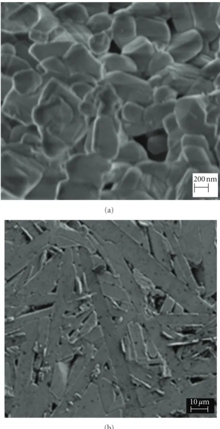
The field emission scanning electron micrograph (FESEM) of BiT powder and the sintered pellet are shown in Figure 2, which shows that extensive grain growth has occurred, leading to platelet formation of the order of 200 nm to 10µm. The platelets of BiT form a brick-wall-like structure by aligning on top of each other, as expected with less platelets damaged during sample preparation.
In our research, we also investigated the new aspect of the development and utilization of the Agilent 85070B
200 nm
(a)
10 µm
(b)
Figure2: FESEM image of BiT: (a) calcined powder at 750◦C for 3 hours and (b) sintered bulk ceramic at 1100◦C for 3 hours.
high-temperature dielectric probe kit in measuring the permittivity of the BiT ceramic material. The frequency dependence of permittivity for BiT ceramic,ε′, is shown in Figure 3. As can be seen, the parameter has a strong depen-dence on frequency, with the permittivity decreasing as frequency increases; however, for the frequency range of 2 to 3 GHz, the permittivity of BiT was on average 21, as shown inTable 1.
3. BiT Array Antenna Design and Structures
4 6
Figure3: Permittivity of BiT ceramic at 1 to 10 GHz.
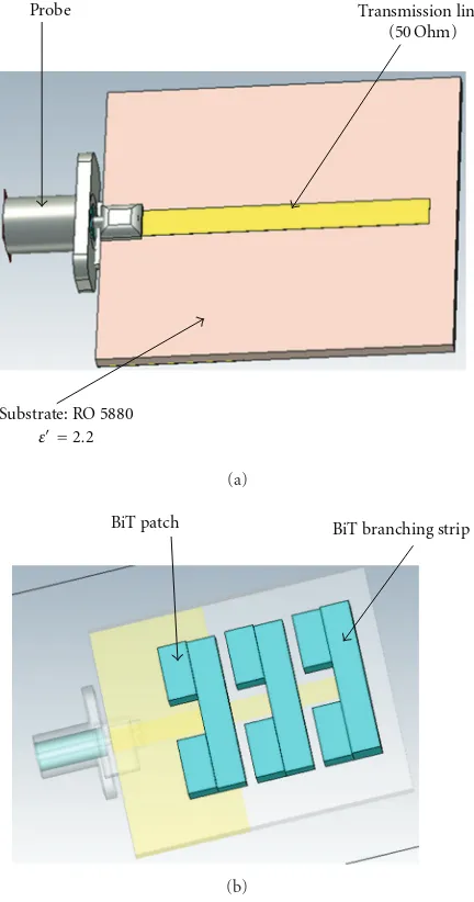
Probe Transmission line
(50 Ohm)
Substrate: RO 5880
ε=2.2
(a)
BiT patch BiT branching strip
(b)
Figure 4: Configuration of the multilayers and its optimized
dimensions, (a) first layer, (b) second layer.
Table1: Permittivity of BiT at frequency 2 to 3 GHz.
Frequency, GHz Permittivity,ε′
2.0800 21.0469
a conducting material, in order to function as a feeding channel.
For the second layer of this investigation, the effectiveness of BiT was determined as a radiating element itself. The nov-elty of this design is the BiT ceramics with high permittivity and low loss. The attenuation due to the conductor can be simplified as:
αc= 8.68Rs
WZ (dB/cm), (1)
whereRsis the surface resistivity and is given by:
Rs=
The attenuation due to dielectric material can be given by the following formula [2]:
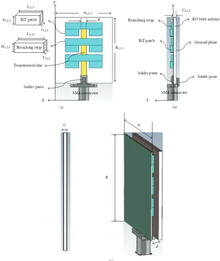
X Y
A1,2,3
B1,2,3
SMA connector Transmission line
BiT patch
Solder paste Branching strip
K l1,2,3
h1,2,3
t1,2,3
L1,2,3
T1,2,3
H1,2,3
(a)
Y
Ground plane
Solder paste Solder paste
SMA connector
RO 5880 substrate Branching strip
BiT patch
C1,2,3
(b)
A
B C
d
(c)
Figure5: Geometry layout of proposed BiT array antenna (a) front (b) side views (c) stacked dielectric layer.
optimized toK =4.6 mm in order to achieve the best 50Ω input impedance matching.
The number of elements and the wavelength of the ceramic array antenna,λgwere approximated using:
λg= λ0 √
nε′, (5)
whereλg is the guided wavelength in CA,λ0is the freespace wavelength,ε′is the dielectric constant of the ceramic, and ndenotes the number of ceramic elements. Hence, (5) shows
that the higher the number of ceramic elements, the smaller the size of the array antenna obtained. In addition, optimiza-tion was also carried out for the BiT ceramic dimensions in order to gain the best antenna performance.
The optimal antenna size for the quantity of two elements BiT isA1=30 mm,B1=33 mm, andC1=1.6 mm. The pa-rameter of BiT branching strip and patches areH1=2.5 mm,
L1=27 mm,T1=1 mm andh1=2.5 mm,l1=4.5 mm, and
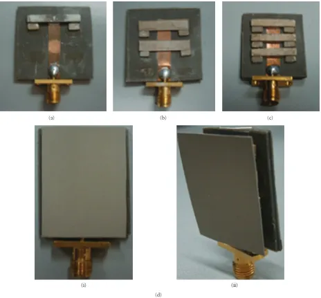
(a) (b) (c)
(i) (ii)
(d)
Figure6: Photograph of fabricated BiT array antennas (a) two BiT ceramic elements (b) four BiT ceramic elements (c) six BiT ceramic elements (d) dielectric layer (i) front view (ii) perspective view.
edge of the BiT patch size beingh2 =2.5 mm,l2=3.5 mm, andt2=0.8 mm; the length,l2, had been reduced 33% from the two elements of BiT antenna, while the BiT array antenna sizes for the four elements areA2 = 27 mm,B2 = 29 mm, andC2 =1.6 mm, which are on average 3 mm smaller than the two elements of BiT antenna. Branching strip dimensions were optimized to H2 = 2.5 mm,L2 = 25 mm, andT2 = 1 mm to obtain good radiation properties. Lastly, the size of the six-element BiT antenna can be observed as the smallest compared to both the two- and four-BiT elements of the BiT array antenna, which areA3 = 22 mm, B3 = 25 mm, and
C3=1.6 mm, and each of the BiT patch element sizes ish3= 2.5 mm,l3 = 3 mm,t3 = 0.8 mm, while the BiT branching strip isH3 =2.5 mm,L3=20 mm, andT3=1 mm. Besides the modeling design, the prototype of the BiT array antennas were fabricated and measured, as can be seen in Figure 6.
This aimed to ensure a good agreement in performance between them.
In designing the BiT array antenna and the dielectric layer stacked as well, one must consider the possibility of high loss performed by the antenna. Numerical simulation shows high levels of the conduction loss and power loss with the utilization of the metallic structure on the antenna. Therefore, BiT array antennas were designed with low-loss BiT elements present with negligible metallic loss in antenna structure to reduce the loss factor that will lead to low antenna performance.
4. Dielectric Layer Design
0
−5
−10
−15
−20
−25
−30
−35
1.8 2 2.2 2.4 2.6 2.8 3 3.2
Simulation with 2 BiT elements Simulation with 4 BiT elements Simulation with 6 BiT elements Measurement with 2 BiT elements Measurement with 4 BiT elements Measurement with 6 BiT elements
R
eflecti
vit
y (dB)
Frequency (GHz)
(a)
−5
−10
−15
−20
−25
1.8 2 2.2 2.4 2.6 2.8 3 3.2
R
eflecti
vit
y (dB)
Frequency (GHz)
Simulation without dielectric layer Measurement without dielectric layer Simulation with dielectric layer Measurement with dielectric layer
(b)
Figure7: Simulated and measured reflectivity of the proposed BiT array antennas (a) two-, four-, and six-BiT element array antenna (b) with and without the dielectric layer.
(a)
−14
−10 −6 −4
−2 0 1 2 3 5 6
(b)
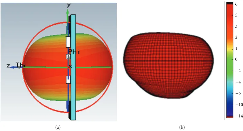
Figure8: Radiation pattern of BiT in 3D view (a) simulated (b) measured.
using multiple dielectrics [7–9]. It has been reported that high gain and high directivity can be achieved if the substrate and dielectric layer are used appropriately [9].
In order to obtain high gain and directivity of this antenna, a suitable dielectric layer of appropriate thickness and loss tangent is chosen. Thinner dielectrics which help to reduce weight also able to reduce the surface wave losses. The dielectric’s dielectric constant, ε′, plays an important role similar to that of the dielectric’s thickness. A low value ofε′
for the dielectric will increase the fringing field of the patch and thus the radiated power. A low-loss tangent reduces the dielectric loss and therefore increases the antenna efficiency. Thus, the dielectric parameters so chosen are Tarconic CER-10, with a thickness of 0.5 mm, permittivity ofε′=10, and a loss tangent tanδ=0.0004.
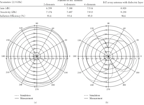
Table2: Gain, directivity, and radiation efficiency of BiT Array Antennas.
Parameters (2.3 GHz) Number of BiT element BiT array antenna with dielectric layer 2 elements 4 elements 6 elements
Gain (dB) 6.559 7.188 7.514 8.920
Directivity (dBi) 7.174 7.697 7.913 9.230
Radiation Efficiency (%) 91.4 93.4 95.0 96.6
0 −5−10−15−20−25−30−35−40−35−30−25−20−15−10−5 0
Figure9: Simulated and measured 2D radiation plot for a six-BiT element array antenna at 2.30 GHz (a) horizontal plane (b) vertical plane.
which is the optimum distance at which to obtain high gain and high directivity. This paper experimentally investigates the effect of a dielectric layer as the superstrate layer for high gain and high directivity on the six elements of BiT array antenna and the comparison between BiT array antenna with and without the dielectric layer.
5. Results and Discussion
The performance of the simulated BiT array antennas with and without the dielectric layer is analysed using Computer Simulation Technology (CST) Microwave Studio, while the fabricated BiT array antennas with and without the dielectric layer were tested using a network analyser and a near-field test facility.Figure 7(a)shows a graph of reflectivity of two-, four-, and six-element BiT array antenna, which had been converted into log magnitude in dB.
The simulation and measurement results show that the reflectivity is the lowest at−27 dB at the centre frequency of 2.40 GHz for BiT array antenna without the dielectric layer. However, with the stackedness of the dielectric layer on BiT
array antennas, the frequency had been shifted to a lower frequency of 2.30 GHz. The frequency shift is also occurring when the number of BiT elements increases from a two-element to a six-two-element array antenna, as can be seen in Figure 7(b). This condition occurs due to the capacitive effects of placing the dielectric over the antenna.
The operating bandwidth of the proposed BiT array antennas for both with and without the dielectric layer was found to be about 350 MHz and 500 MHz, respectively, which is compatible with the specification of the WiMAX system. Overall, good agreements were found between the simulation and measurement results, although there was slight discrepancy between them, believed to be due to the environmental effect and mechanical tolerance, which were neglected in our simulations.
the point of strongest signal, thus avoiding signal redundancy and interference with other antennae radiating at the same plane.
Figure 9shows the radiation pattern of a six-element BiT array antenna in 2D view, which was analyzed in vertical plane (XZ, YZ) and in horizontal plane (XY) at 2.30 GHz. This antenna provides a 360-degree coverage signal, which is in all directions (horizontally) for two-way communication. From Table 2, the gain of the six-element BiT array antenna, in radiation patterns, with dielectric layer does exhibit 8.920 dB and 9.230 dBi of gain and directivity, respectively. The simulation results show that the gain of the 4-element BiT array antenna has improved greatly compared to the common antenna.
6. Conclusions
In this paper, the application of rectangular bismuth titanate (BiT) material as a ceramic antenna (CA) in array form, which composed of two-, four-, and six-element BiT as well as a stacked dielectric layer, were investigated and successfully carried out. The antenna exhibited acceptable bandwidths, reflectivity, and radiation characteristics for WiMAX applica-tion. As a result, we find that BiT array antennas are attractive and can be practical for various systems. By taking into account all of the details of each component, including the dimensions and permittivity value, the antennas did perform up to expectation when the number of BiT element increased at the WiMAX band. In future work, bismuth titanate (BiT) can be investigated for other types of antenna in order to determine the level of performance improvement in term of bandwidth particularly in an optimized radiation pattern. In addition, antenna enhancement can be done by adjusting the distanced, and the resonance condition for high gain as well as high directivity can be obtained.
References
[1] M. F. Ain, S. I. S. Hassan, J. S. Mandeep et al., “2.5 GHZ batio3 dielectric resonator antenna,” Progress in Electromagnetics Research, vol. 76, pp. 201–210, 2007.
[2] C. A. Balanis, Antenna Theory: Analysis and Design, Wiley Interscience, Hoboken, NJ, USA, 3rd edition, 2005.
[3] S. Prabhu, J. S. Mandeep, and S. Jovanovic, “Microstrip band-pass filter at S band using capacitive coupled resonator,”Progress in Electromagnetics Research, vol. 76, pp. 223–228, 2007. [4] R. K. Mongia, A. Ittipiboon, and M. Cuhaci, “Measurement
of radiation efficiency of dielectric resonator antennas,”IEEE Microwave and Guided Wave Letters, vol. 4, no. 3, pp. 80–82, 1994.
[5] A. A. Kishk, X. Zhang, A. W. Glisson, and D. Kajfez, “Numerical analysis of stacked dielectric resonator antennas excited by a coaxial probe for wideband applications,”IEEE Transactions on Antennas and Propagation, vol. 51, no. 8, pp. 1996–2006, 2003. [6] A. A. Kishk, “Wide-band truncated tetrahedron dielectric
res-onator antenna excited by a coaxial probe,”IEEE Transactions on Antennas and Propagation, vol. 51, no. 10, pp. 2913–2917, 2003.
[7] M. T. Lee, K. M. Luk, K. W. Leung, and M. K. Leung, “Small dielectricresonator antenna,” IEEE Transactions on Antennas and Propagation, vol. 50, pp. 1485–1487, 2002.
[8] J. Clerk Maxwell,A Treatise on Electricity and Magnetism, vol. 2, Clarendon, Oxford, UK, 3rd edition, 1892.
[9] S. Sreekantan, A. F. M. Noor, Z. A. Ahmad, R. Othman, and A. West, “Structural and electrical characteristic of crystalline bar-ium titanate synthesized by low temperature aqueous method,”