Pengaruh Pemanasan Terhadap Morfologi Permukaan dan
Ukuran Grain pada Lapisan Tipis Tembaga Sebagai Katalis pada
Penumbuhan Graphene
A Study of the Effect of Thermal Annealing on the Morphology
Surface and Grain Size of Thin Copper Films as Catalyst for
Graphene Growth
Kasman*
Jurusan Fisika Fakultas MIPA Universitas Tadulako
ABSTRACT
The effect of thermal annealing on the morphology surface and grain size of thin copper films was studied. The purpose of this study is to find an optimal annealing condition in obtaining a copper catalyst, having a smooth surface with a large grain size. Such catalyst is potential to grow a high quality graphene film. In this work, the copper film (99.99+ % purity; 500 nm thick) was employed by varying annealing temperature (450-900 °C), annealing time (0-1200 min) and hydrogen flow rate (0-100 sccm). These copper catalysts were further studied by means of XRD, SEM and EDS analysis to know their structural properties. XRD results revealed that this copper film has a good nanocrystalline cubic structure, dominated by (111) plane. SEM results showed that the 900 oC- annealed copper film has larger grain size (~ 1.3 µm) than the others. EDS analysis showed the presence of copper oxide peaks on the annealed copper under hydrogen-free atmosphere, indicating the importance of hydrogen gas for removing the copper oxide impurities. Based on those studies above, the optimal annealing condition for obtaining a copper substrate with the smooth surface and large grain size is by annealing at 450 °C for 20 hours under hydrogen flow rate of 50 sccm.
Keywords : Thin copper film, Thermal annealing, grain size.
ABSTRAK
Pengaruh Pemanasan Terhadap Morfologi Permukaan dan Ukuran Grain pada lainnya. Hasil analisis EDS menunjukkan adanya puncak-puncak tembaga oksida pada sampel yang tidak dialirkan gas hydrogen, yang berarti bahwa gas hidrogen sangat berperan dalam mengeliminir impurity dari tembaga oksida. Berdasarkan hasil-hasil pengujian di atas maka kondisi optimal dalam pemanasan lapisan tipis tembaga sebagai katalis pada penumbuhana graphene adalah pemanasan pada 450 °C selama 20 jam dengan laju aliran hydrogen sebesar 50 sccm.
Kata Kunci : Lapisan tipis tembaga, Pemanasan, morfologi permukaan, Ukuran grain.
INTRODUCTION
In the last few years, copper foil has attracted considerable interest in both academic and industrial communities since the report of large-area graphene thin films for conductive and transparent electrodes (Bae et al., 2010; Kim et al., 2009 and Li et al., 2009). However, some practical complications are involved when using copper foil as the catalyst. For example, it
takes quite a number of hours to etch away the copper foil as the thickness of a copper
foil is generally in the range of tens micrometres. The etching of different Cu catalyst thicknesses (12.5, 25 and 50 µm) was conducted by Xuesong Li, et al. [4] showing that the etching time was a function of thickness. Furthermore, it normally requires a transfer step which uses PMMA as the transfer agent, which is very hard to wash off completely once the graphene film is transferred to a substrate and can lead to contamination to some degree.
To eliminate the transfer step, much
thinner (hundreds of nanometres) copper thin films are more desirable. These copper thin films can be easily deposited to selected substrates and be etched away quickly without the need for a transfer step. Annealed copper foils preferentially form as a Cu(100) crystalline face (Wofford et al., 2010), while thermally grown copper thin films lead to prefer in the Cu(111) crystalline orientation. These different crystalline structures lead to different graphene growth which has been reported by Ruoff etc. Further work by Pasupathy [6] also reported that a single crystal Cu(111) face is superior to a Cu(100) face to grow more uniform graphene sheets.
thin films during the pre-treatment before the graphene growth.
MATERIAL AND METHOD
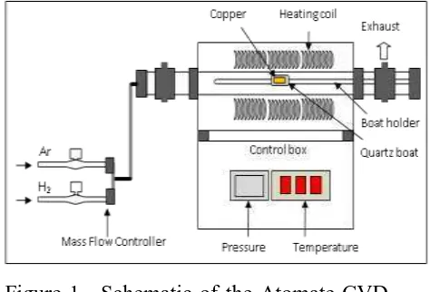
To prepare a catalyst with high quality for growing graphene, a kind of copper, i.e. thin copper film (99.99+ % purity; 500 nm thick), was employed for studying the effects of thermal annealing on its microstructure, by varying annealing temperature (450-900 °C), annealing time
1200 min) and hydrogen flow rate (0-100 sccm). All these experiments were conducted in an Atomate CVD furnace (Fig. 1) by introducing a mixture of H2/Ar (50 and 100 sccm, respectively) gas under a pressure of 500 mTorr, except for the study of the variation of hydrogen flow rate. The introduction of hydrogen gas is desired to reduce copper oxides which may occur on the surface, while argon gas is applied to remove H2O steam as reaction products or unwanted gases. Properties of the studied samples were characterised by using X-ray diffraction (XRD) for the crystal structure and scanning electron microscopy (SEM) for the morphological surface, while EDS
analysis was used to confirm the presence of copper oxide on the hydrogen-free
flowed sample
Figure 1. Schematic of the Atomate CVD furnace used for annealing the copper.
RESULT AND DISCUSSION
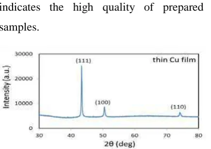
XRD measurements were used to study the effect of annealing on the microstructure of copper substrate. In this technique, a CuKα radiation source (λ = 1.54056 Å) was employed and the
indicates the high quality of prepared samples.
Figure 2 XRD spectra of the as-evaporated thin copper film
Effect of Annealing Temperature
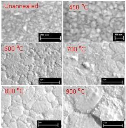
Five different annealing temperatures (450, 600, 700, 800, 900 oC) for the fixed time and hydrogen flow rate of 1 hour and 50 sccm.were employed to study the effect of annealing temperature on the microstructure of thin copper substrate. These samples were characterised by using XRD (Fig. 3a) and SEM (Fig. 3b).
Figure 3a. XRD profiles of the thin copper films annealed at different temperatures
Figure 3a shows XRD profiles of the as-evaporated and annealed thin copper films with three major reflections from (111), (100), and (110) planes at the angle of 43.4°, 50.6° and 74.2°, respectively. From this figure, it is found that the
diffraction peak of (111) plane on the samples is more intense than that of (100) and (110) planes. This observation indicates that the crystal structure with a (111) plane is more favourable than the others. However, the intensity of this plane increases after annealing, indicating the formation of larger grain structures, consistent with the previous report by Vinci et al. ( Zielinski et al., 1994). A very strong (111) intensity is detectable when the sample is annealed at 900 oC. This peak increase is due to further re-crystallisation with a much larger grain size. On the other hand, the peak of the (110) plane exhibits no significant change indicating that the thermal annealing treatment does not cause a formation of other grain textures.
To confirm the change of (111) diffraction peaks on the thin copper film, observations were made in the SEM images of the films. Figure 3b shows that a noticeable grain growth on the thin copper films is clearly observed after annealing at temperatures above 700 oC. In fact, at 800 oC, grain structures clearly appear with a dominant size of around 0.6 µm. A much larger grain size of around 1.3 µm occurs at 900 oC. This observation confirms that it is the large grain size that is strongly associated with the high intensity diffraction peak, shown in Figure 3a.
Figure 3b SEM images of the thin copper films annealed at different temperatures.
Effect of Annealing Time
In order to study the effect of annealing time on the microstructure of copper catalysts, thin copper films were further studied by annealing for various annealing times (0, 1, 3, 5, 10, and 20 hours) at the fixed temperature and hydrogen flow rate of 450 oC and 50 sccm. The main reason behind the selection of the low annealing temperature was that the film was evaporated on a glass substrate that undergoes mechanical changes over 450 oC. These samples were characterised by using XRD (Fig. 4a) and SEM (Fig. 4b).
Figure 4a. XRD profiles of the copper films
Figure 4a shows XRD patterns of the samples annealed for three different times of 2, 5 and 20 hours. In this figure, it appears that the intensity of (111) diffraction peak systematically increases with increasing annealing time. This is an indicator that increased recrystalisation occurs on the samples annealed for longer times.
Figure 4b. SEM images of the copper films annealed for different times.
Effect of Hydrogen Flow Rate
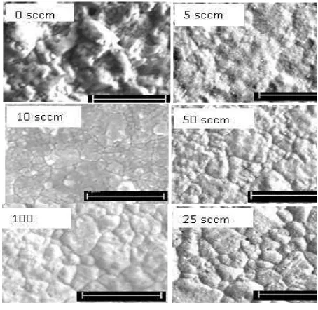
To determine the influence of hydrogen gas on the formation of morphological structure on copper’s surface, the copper substrate was studied by annealing under various flow rates of 0, 5, 10, 25, 50 and 100 sccm with a fixed annealing temperature and time of 450 oC and 1 hour, respectively. The goal of this study is to find an optimal hydrogen flow rate for resulting in a smooth surface of the substrates.
Figure 5 SEM images of thin copper film at 450 oC for 1 hour under different irregular shapes and sizes when introducing a hydrogen flow rate above 10 sccm. The grains are not clearly observable on the samples introduced with 5 sccm and without hydrogen gas, and the hydrogen-free treated film surface is much rougher than that of the 5 sccm-treated surface. This roughness may be caused by the presence
of a thin oxide layer. This study shows that the 1 hour-treated hydrogen flow rates do not form a larger grain, meanwhile, the large grain size can facilitate the growth of large graphene flakes (Mattevi et al., 2011). In comparison, the grain size of the 20 hours-annealed thin Cu film with the fixed hydrogen flow rate of 50 sccm (see Figure 4b) was much larger than that of the 1 hour-annealed thin Cu film with the varied hydrogen flow rates (see Figure 5). This reveals that the best condition to prepare the thin copper film as catalyst for graphene growth is by annealing at the temperature of 450 oC for 20 hours under the hydrogen flow rate of 50 sccm.
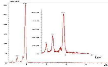
Figure 6a EDS analysis of the thin copper film annealed at 450 oC under the hydrogen-free atmosphere.
Figure 6b XRD profile of the thin copper film annealed at 450 oC under the hydrogen-free atmosphere.
Crystallite and Grain Sizes
To get a deeper insight into the influence of annealing on the copper microstructure, the crystallite size of the grains in thin copper films was calculated by using the Debye-Scherrer formula as follows (Patterson, 1939):
cos
9 . 0
D
(1)
where, λ is the wavelength of the incident X-rays (0.154056 nm for Cu Kα1), β the half width of diffraction peak measured in radians, and θ the diffraction angle. While, the determination of grain sizes on the
intercept count method of ASTM E112, which is based on the number of grain boundary intersections per unit length, PL. This unit isa random test line that produces on statistically representative sections (Abrams, 1971). Mathematically, it is defined as:
M L
P P
T i L
(2)
where Pi is the number of grain boundary
intersections counted on the test line, LT is the total test length and M is the magnification.
In this study, the calculation of crystallite and grain sizes was carried out on thin copper films annealed at different temperatures (see subsection 3.1). The average crystallite and grain sizes calculated are plotted in Figure 7.
Figure 7 Crystallite and grain sizes on thin copper film as a function of annealing temperature.
after annealing beyond 450 oC. The average crystallite size resulted is ~ 100 nm. This result shows that annealing provides larger crystallites compared to the original size. The grains of the unannealed thin Cu film are observed to be ~ 0.05 µm in size. An increase of grain size occurs when annealed beyond 600 oC and more significantly increases when annealed at 900 oC with ~ 1.3 µm in size.
By studying the effect of the annealing temperature, annealing time and hydrogen flow rate on thin copper film in forming a grain structure, a combination of the parameters for was selected to be an annealing temperature at 450 oC for 20 hours under hydrogen flow rate of 25 sccm. The choice of this low temperature is due to the use of glass as a substrate in evaporating thin copper film. Glass undergoes mechanical changes, such as bending, when annealed above 450 oC and even melts when annealed above 550 oC.
This paper has presented a study of the effect of thermal annealing on the morphology of thin copper film as catalyst for graphene growth. As-evaporated thin copper film was annealed with various temperatures, times, hydrogen flow rate for studying the change of structural and morphological properties. The film was annealed firstly at 450 to 900˚C for a time and hydrogen flow rate of 1 hour and 50 sccm, respectively, then for 1 to 20 hours at the fixed temperature and hydrogen flow
nanocrystalline cubic structure, dominated by (111) plane. The SEM results show that the sample annealed at 900 oC has smoother surface morphology with uniform coverage and larger grain size (~ 1.3 µ m) than the others. The EDS analysis showed the presence of copper oxide peaks on the annealed copper under hydrogen-free atmosphere This analysis indicates that the hydrogen gas is crucial for removing the copper oxide impurities.
ACKNOWLEDGEMENT
The author would like to thank the Indonesian Directorate General of Higher Education (DIKTI) for financing in doing this work. I am also grateful to all of the members of the Center for Organic Electronics (COE) for useful discussions and support during this work, especially my supervisor, Prof. Dr. Paul dastoor, and Co-supervisors, Dr. Warwick Belcher and Dr.
Xiaojing Zhou.
REFERENCES
Abrams, H., 1971, Grain size measurement by the intercept method, Metallography 4 : 59-78.
Bae, S., H., et al., 2010, 30 inch roll-based production of high-quality graphene films for flexible transparent electrode,. Nat. Nanotech.
Kim, J. Y. Choi, and B. H. Hong, 2009, Large-scale pattern growth of graphene films for stretchable transparent electrodes. Nature 457(7230) : 706-710.
Li, X., et al., 2009, Ruoff, Large-area synthesis of high-quality and uniform graphene films on copper foils. Science 324 : 1312-1314.
Li, X., Y. Zhu, W. Cai, M. Borysiak, B. Han, D. Chen, R. D. Piner, L. Colombo and R. S. Ruof, 2009, Transfer of large-area graphene films for high-performance transparent conductive electrodes. Nano Lett. 9(12) : 4359-4363.
Mattevi, C., H. Kim and M. Chhowalla, 2011, A review of chemical vapour deposition of graphene on copper. J. Mater. Chem. 21(10) : 3324-3334.
Miculescu, F., I. Jepu, C. Porosnicu, C. P. Lungu, M. Miculescu, and B. Burhala, 2011, A study on the influence of the primary electron beam on nanodimensional layers analysis, Digest J. Nanomater. Biostruct. 6(1) : 307-317.
Patterson, A.L., 1939, The Scherrer formula for X-ray particle size determination, Phys. Rev. 56 : 978.
Swanson, T., 1953, Powder diffraction data. National Bureau Standard, Circ. 539(I) : 15.
Thouless, M.D., J. Gupta, and J. M. Harper, 1993, Stress development and relaxation in copper films during thermal cycling. J. Mater. Res. 8 : 1845.
Wofford, J.M., S. Nie, K. F. McCarty, N. C. Bartelt, and O. D. Dubon, 2010, Graphene islands on Cu foils: The interplay between shape, orientation, and defects, Nano Lett. 10 : 4890-4896.
Yin, M., C. K. Wu, Y. Lou, C. Burda, J. T. Koberstein, Y. Zhu, and S. O’Brien, 2005, Copper Oxide nanocrystals, J. Am. Chem. Soc. 127 : 9506-9511.
Zhaoa, L., K.T. Rimb, H. Zhoua, R. Hea, T. F. Heinz, A. Pinczuk, G. W. Flynn, and A.N. Pasupathy, 2011, Influence of copper crystal surface on the CVD growth of large area monolayer graphene. Solid State Commun. 151 : 509-513.