Practices and Pitfalls
Analog
Boca Raton London New York Washington, D.C. CRC Press
James C. Daly
Department of Electrical and Computer Engineering
University of Rhode Island
Denis P. Galipeau
Cherry Semiconductor Corp.
Practices and Pitfalls
Analog
Foreword
This book presents practical methods and pitfalls encountered in the design of biCMOS integrated circuits. It is intended as a reference for design engineers and as a text for an introductory course on analog integrated circuit design for engineering seniors and graduate students. Abroad range of topics are covered with the intent of giving new designers the tools to complete a design project. Most of the topics have been simplified so they can be understood by students who have had a course in electronics.
The material has been used in a course open to seniors and graduate students at the University of Rhode Island. In the course, students were required to design an analog integrated cir-cuit that was fabricated by Cherry Semiconductor Corporation.
In the process of assembling material for the book, we had dis-cussions with many people who have been generous with informa-tion, ideas and criticism. We are grateful to James Alvernez, Mark Belch, Brad Benson, Mark Crowther, Vincenzo DiTommaso, Jeff Dumas, Paul Ferrara, Godi Fischer, Justin Fisher, Robert Fugere, Brian Harnedy, David Harrington, Ashish Kirtania, Seok-Bum Ko, Shawn LaLiberte, Andreas Ladas, Sangmok Lee, Eric Lind-berg, Jien-Chung Lo, Robert Maigret, Nadia Matchey, Andrew McKinnon, Jay Moser, Ted Neira, Peter Rathfelder, Shelby Ray-mond, Jon Rhan, Paul Sisson, Michael Tedeschi, Claudio Tuoz-zolo, and Yingping Zheng.
Finally, we owe our thanks to the management and engineering staff of Cherry Semiconductor Corporation. CSC has fabricated scores of analog IC designs generated by the URI students enrolled in the course that has been the basis for this book.
Contents
1 Devices
1.1 Introduction
1.2 Silicon Conductivity
1.2.1 Drift Current
1.2.2 Energy Bands
1.2.3 Sheet Resistance
1.2.4 Diffusion Current
1.3 Pn Junctions
1.3.1 Breakdown Voltage
1.3.2 Junction Capacitance
1.3.3 The Law of the Junction
1.3.4 Diffusion Capacitance
1.4 Diode Current
1.5 Bipolar Transistors
1.5.1 Collector Current
1.5.2 Base Current
1.5.3 Ebers-Moll Model
1.5.4 Breakdown
1.6 MOS Transistors
1.6.1 Simple MOS Model
1.7 DMOS Transistors
1.8 Zener Diodes
1.9 EpiFETs
1.10 Chapter Exercises 2 Device Models
2.1 Introduction
2.2 Bipolar Transistors
2.2.1 Early Effect
2.2.2 High Level Injection
2.2.3 Gummel-Poon Model
2.3 MOS Transistors
2.4 Simple Small Signal Models for Hand Calculations
2.4.1 Bipolar Small Signal Model
2.4.2 Output Impedance
2.4.3 Simple MOS Small Signal Model
2.5 Chapter Exercises 3 Current Sources
3.1 Current Mirrors in Bipolar Technology
3.2 Current Mirrors in MOS Technology Chapter Exercises
4 Voltage References
4.1 Simple Voltage References
4.2 Vbe Multiplier
4.3 Zener Voltage Reference
4.4 Temperature Characteristics ofIc andVbe 4.5 Bandgap Voltage Reference
5 Amplifiers
5.1 The Common-Emitter Amplifier
5.2 The Common-Base Amplifier
5.3 Common-Collector Amplifiers (Emitter Followers)
5.4 Two-Transistor Amplifiers
5.5 CC-CE and CC-CC Amplifiers
5.6 The Darlington Configuration
5.7 The CE-CB Amplifier, or Cascode
5.8 Emitter-Coupled Pairs
5.9 The MOS Case: The Common-Source Amplifier
5.10 The CMOS Inverter
5.11 The Common-Source Amplifier with Source Degeneration
5.12 The MOS Cascode Amplifier
5.13 The Common-Drain (Source Follower) Amplifier
5.14 Source-Coupled Pairs
5.15 Chapter Exercises 6Comparators
6.1 Hysteresis
6.1.1 Hysteresis with a Resistor Divider
6.1.2 Hysteresis from Transistor Current Density
6.1.3 Comparator withVbe-Dependent Hysteresis
6.2 The Bandgap Reference Comparator
6.3 Operational Amplifiers
6.4 A Programmable Current Reference
6.5 A Triangle-Wave Oscillator
6.6 A Four-Bit Current Summing DAC
6.7 The MOS Case
6.8 Chapter Exercises 7 Amplifier Output Stages
7.1 The Emitter Follower: a Class A Output Stage
7.2 The Common-Emitter Class A Output Stage
7.3 The Class B (Push-Pull) Output
7.4 The Class AB Output Stage
7.5 CMOS Output Stages
7.6 Overcurrent Protection
7.7 Chapter Exercises 8 Pitfalls
8.1 IR Drops
8.1.1 The Effect of IR Drops on Current Mirrors
8.2 Lateral pnp
8.2.1 The Saturation of Lateral pnp Transistors
8.2.2 Low Beta in Large Area Lateral pnps
8.3 npn Transistors
8.3.1 Saturating npn Steals Base Current
8.3.2 Temperature Turns On Transistors
8.4 Comparators
8.4.1 Headroom Failure
8.4.2 Comparator Fails When Its Low Input Limit Is Exceeded
8.4.3 Premature Switching
8.5 Latchup
8.5.1 Resistor ISO EPI Latchup
8.6 Floating Tubs
8.7 Parasitic MOS Transistors
8.7.1 Examples of Parasitic MOSFETs
8.7.2 OSFETs
8.7.3 Examples of Parasitic OSFETs
8.8 Metal Over Implant Resistors 9 Design Practices
9.1 Matching
9.1.1 Component Size
9.1.3 Temperature
9.1.4 Stress
9.1.5 Contact Placement for Matching
9.1.6 Buried Layer Shift
9.1.7 Resistor Placement
9.1.8 Ion Implant Resistor Conductivity Modulation
9.1.9 Tub Bias Affects Resistor Match
9.1.10 Contact Resistance Upsets Matching
9.1.11 The Cross Coupled Quad Improves Matching
9.1.12 Matching Calculations
9.2 Electrostatic Discharge Protection (ESD)
9.3 ESD Protection Circuit Analysis
chapter 1
Devices
1.1
Introduction
The properties and performance of analog biCMOS integrated circuits are dependent on the devices used to construct them. This chapter is a review of the operation of silicon devices. It begins with a discus-sion of conductivity and resistance. Simple physical models for bipolar transistors, MOS transistors, and junction and diffusion capacitance are developed.
1.2
Silicon Conductivity
The conductivity of silicon can be controlled and made to vary over several orders of magnitude by adding small amounts of impurities. Sil-icon belongs to group four in the periodic table of elements. It has four valence electrons in its outer shell. A silicon atom in a silicon crystal has four nearest neighbors. Silicon forms covalent bonds where each atom shares its valence electrons with its four nearest neighbors. Each atom has its four original valence electrons plus the four belonging to its neighbors. That gives it eight valence electrons. The eight valence electrons complete the shell producing a stable state for the silicon atom. Electrical conductivity requires current consisting of moving electrons. The valence electrons are attached to an atom and are not free to move far from it. Some valence electrons will receive enough thermal energy to free themselves from the silicon atom. These electrons move to energy levels in a band of energy called the conduction band. Conduction band electrons are not attached to a particular atom and are free to move about the crystal.
electronic charge associated with it. With one electron gone, there are seven valence electrons, shared with nearby neighbor atoms, and one hole associated with the ionized silicon atom. Holes can move. If the hole represents a missing electron that was shared with the silicon neigh-bor on the left, only a small amount of energy is required for one of the other seven valence electrons to move into the hole. If an electron shared with an atom on the right moves into the hole on the left, the hole will have moved from the left of the atom to the right. The movement of holes in silicon is really the movement of electrons leaving and filling electron states. It is like the motion of a bubble in a fluid. The bubble is the absence of the fluid. The bubble appears to move up, but actually the fluid is moving down. Each hole in silicon is a mobile positive charge equal to one electronic charge.
Figure 1.1 A schematic representation of a silicon crystal is shown. Each silicon atom shares its four valence electrons with its nearest neighbors. A positively charged “hole” exists where an electron has been lost due to ioniza-tion. The hole acts as a mobile positive particle with a charge equal to one electronic charge.
The conductivity of silicon increases when there are more charge car-riers (electrons and holes) present. In pure silicon there will be a small number of thermally generated electron hole pairs. The number of elec-trons equals the number of holes because each electron leaving a sili-con atom for the sili-conduction band leaves behind a hole in the valence band. When the number of holes equals the number of conduction elec-trons, this is called intrinsic silicon. The intrinsic carrier concentration is strongly temperature dependent. At room temperature, the intrinsic carrier concentrationni = 1.5x10¹⁰ electron-hole pairs/cm3.
electrons form covalent bonds with its four silicon neighbors. The re-maining phosphorus electron is loosely associated with the phosphorus atom. Only a small amount of energy is required to ionize the phospho-rus atom by moving the extra electron to the conduction band leaving behind a positively ionized phosphorus atom. Since an electron is added to the conduction band, the added group five impurity is called a donor. This represents n-type silicon with mobile electrons and fixed positively ionized donor atoms. N-type silicon is typically doped with 1015or more donors per cubic centimeter. This swamps out the thermally generated electrons at normal operating temperatures.
A group three element, like boron, is called an acceptor. Doping with acceptors results in p-type silicon. When an acceptor element with three valence electrons in its outer shell replaces a silicon atom, it becomes a negative ion, acquiring an electron from the silicon. That allows it to complete its outer shell and to form covalent bonds with neighboring sil-icon atoms. The electron acquired from the silsil-icon leaves a hole behind. At room temperature all acceptors are ionized and the number of holes per cubic centimeter is equal to the number of acceptor atoms.
In an n-type semiconductor, electrons are the majority carriers and holes are referred to as minority carriers. Similarly, in p-type semicon-ductors, holes are the majority carriers and electrons are referred to as minority carriers. In practical devices, doping levels greatly exceed the thermally generated levels of electron hole pairs (by 5 orders of mag-nitude or more). When silicon is doped, say, with donors to produce n-type silicon, the number of holes is reduced. The large number of electrons increases the probability of a hole recombining with an elec-tron. An equilibrium develops where the increase of holes due to ther-mal generation equals the decrease of holes due to recombination. The recombination rate and the number of holes varies inversely with the number of electrons. This is called the law of mass action. It holds for all doping levels in both p-type and n-type semiconductors in equilib-rium. It is a very useful relationship that allows the number of minority carriers to be calculated when the doping level for the majority carriers is known. The law of mass action is
pn=n2
i (1.1)
where p is the number of holes per cubic cm and n is the number of conduction electrons per cubic cm.
Example
A silicon sample is doped withND = 5x10¹⁷
donors/cm3
The sample is n-type where electrons are the majority carriers. As-suming all donors are ionized, the electron density is equal to the donor concentration,n= 5x1017cm−3. The minority (hole) concentration is
p= n 2 i ND =
(1.5x10¹⁰ )2
5x1017 = 450cm −3
There are very few holes compared to electrons in this n-type sample.
1.2.1
Drift Current
Voltage across a silicon sample results in an electric field that exerts a force on free electrons and holes causing them to move resulting in current flow. Consider an electron. The force produced by the electric field causes it to accelerate. Its velocity increases with time until it strikes the silicon crystal lattice or an impurity, where it is scattered and loses its momentum. The electron is constantly accelerating then bumping into the silicon losing its momentum. This process results in an average velocity proportional to the electric field called the drift velocity.
vdrif t=µnE (1.2)
whereµnandEare the electron mobility and the electric field. Mobility decreases when there is more scattering of carriers. Lattice scattering in-creases with temperature. Therefore, mobility and conductivity tend to decrease with temperature. Carriers are also scattered from impurities. Mobility decreases significantly with doping as shown inFigure 1.2.[2]. Conductivity is proportional to mobility and carrier concentration. For an n-type sample, the current flowing through the cross-sectional area Ais
I=AqµnE =AσE (1.3) where q is the electronic charge, n is the number of free electrons per cubic centimeter, and σ = qµnn is the conductivity. Since the sam-ple is doped with ND donors per cubic centimeter, n = ND and the conductivity is
σ=qµnND (1.4)
similarly the conductivity of p-type silicon, doped with acceptor atoms, where the current carriers are holes is σ = qµpNA, where NA is the number of acceptor atoms per cubic centimeter.
1.2.2
Energy Bands
Figure 1.2 Carrier mobility in silicon at 300◦Kdecreases significantly with impurity concentration.[1] (Reprinted from Solid-State Electronics, Volume II, S. M. Sze and J. C. Irvin,Resistivity, Mobility and Impurity Levels in GaAs, Ge, and Si at 300◦ K., pages 599-602, Copyright 1968, with permission from Elsevier Science.)
occupied by valence electrons attached to silicon atoms. The conduction band is occupied by conduction electrons that are free to move about the crystal. If all electrons are in their lowest energy states, they are occupying states in the valence band. The difference between the con-duction band edge and the valence band edge isEG= 1.12eV, the band gap. When a silicon atom loses an electron, it takes 1.12 electron volts of energy for the electron to move from the valence to the conduction band. When this happens the conduction band is occupied by an elec-tron and the valence band is occupied by a hole. Impurities introduce electron states inside the band gap close to the valence or conduction band. Donor states are close to the conduction band. It takes very little energy for an electron to move from a donor state to the conduction band. Acceptor states are located close to the valence band. A valence electron can easily move from the valence band to an acceptor state.
The Fermi level is a measure of the probability that a state is occupied by an electron. States below the Fermi level tend to be occupied, while states above it tend to be unoccupied. As the temperature increases, some states below the Fermi level will become unoccupied as electrons move up to levels above the Fermi level. States at the Fermi level have a 50-50 chance of being occupied. In intrinsic silicon where the number of holes equals the number of electrons, the Fermi level is approximately half way between the valence and conduction bands. This Fermi level is called the intrinsic level,Ei. In an n-type semiconductor, with con-duction band states occupied, the Fermi level moves up closer to the conduction band as the probability that a conduction band state is oc-cupied increases. In p-type semiconductors, with vacant valance band states (holes), the Fermi level moves down closer to the valence band.
The position of the Fermi level relative to the intrinsic level is a mea-sure of the carrier concentration. For n-type silicon, the Fermi level,Ef is above Ei. For p-type it is below Ei. The number of electrons per cubic cm in the conduction band is related to the position of the Fermi level by the following equation[3, page 22].
n=nieEf−EiKT (1.5) whereni is the intrinsic carrier concentration andK = 8.62x10⁻⁵ elec-tron volts per degrees Kelvin is Boltzmann’s constant. If T = 300, KT = 0.0259V. 300 degrees Kelvin is 27 degrees C and 80.6◦F, com-monly called room temperature.
Since by the law of mass actionpn=n2 i
Example
If a silicon sample is doped with 1017
acceptors per cm3
, calculate the position of the Fermi level relative to the intrinsic level at room temperature.
At normal operating temperatures, all acceptors will be ionized and the hole concentrationpwill equal the acceptor concentration.
p=NA= 1017
holes percm3 From Equation 1.6:
Ei−Ff =KT ln NA
ni
= 0.0259ln
1017 1.5x1010
= 0.41V
The Fermi level is 0.41V below the intrinsic level.
1.2.3
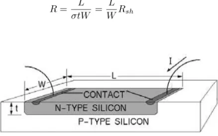
Sheet Resistance
Sheet resistance is an easily measured quantity used to characterize the doping of silicon. Consider the sample shown inFigure 1.4. The silicon is doped with donors to form a resistor of n-type silicon. The resistor length is L and its cross-sectional area is tW, where t is the effective depth of the resistor. The resistance is
R= L
σtW = L
WRsh (1.7)
Figure 1.4 Resistors are formed in silicon by placing dopants in a specific region.
resistance is a process parameter dependent on doping:
Rsh= 1 σt =
1
qµNDt (1.8)
where ND is an average doping. Usually doping varies with distance down from the surface of the silicon. NDt is the number of donors per unit area.
1.2.4
Diffusion Current
The current flow mechanism responsible for the characteristics of diodes and transistors is diffusion. Diffusion current flows without being caused by an electric field. Electrons and holes in semiconductors are in con-stant thermal motion. When there is a nonuniform distribution of carri-ers (electrons or holes), random motion causes a net motion away from the region where the electrons or holes are more dense. Consider the nonuniform distribution of holes shown inFigure 1.5. The charged par-ticles, represented by plus signs, are equally likely to move either to the right or to the left. Because there are more particles on the left there is a net motion of one particle to the right passing across each vertical plane. This situation can exist at a pn junction, where an unlimited supply of free carriers, caused by a forward bias voltage, allows a concentration gradient to be maintained. InFigure 1.5, carrier motion is indicated by the arrows. Random motion is modeled by grouping carriers together in pairs with opposite velocities so the average velocity is zero. The overall result is the movement of one carrier from each region of high concen-tration to the neighboring low concenconcen-tration region. If the distribution of carriers is maintained, there will be a constant current flow from left to right.
The diffusion current density for holes is given by
Jp =−qDpdp
dx (1.9)
whereJp is the current density, amperes/cm2, Dp is the diffusion con-stant andpis the hole density, holes/cm2.
Einstein’s relation shows the diffusion constant for holes to be propor-tional to mobility [3, page 38]:
Dp =µpVT (1.10)
and for electrons
Figure 1.5 The nonuniform distribution of randomly moving positive charges results in a systematic motion of charge. Here a positive current is moving to the right.
where VT =KT /q is the thermal voltage. VT = 26mV at room tem-perature. K is Boltzmann’s constant. q= 1.6x10⁻¹⁹C is the electronic charge andT is the absolute temperature. It is not surprising that the mobility is proportional to the diffusion constant since both describe the motion of charge in the silicon crystal.
1.3
Pn Junctions
Pn junctions are the building blocks of integrated circuit components. They serve as parts of active components, such as the base-emitter or collector-base junctions of a bipolar transistor, or as isolation between components, as is the case when an integrated resistor is fabricated in a reverse-biased tub. Each pn junction has a parasitic capacitance associ-ated with it that affects device performance. Important properties such as breakdown voltage and output resistance are dependent on properties of pn junctions. Since this text isn’t intended to teach device physics, we will review pn junctions only so far as is required to understand transistor operation.
p-region to the n-p-region where they recombine with electrons. This pro-cess leaves positive donor ions in the n-region and negative acceptor ions in the p-region. The donors and acceptors occupy fixed positions in the silicon crystal and cannot move. An electric field exists between the positive donor ions in the n-region and the negative acceptor ions in the p-region. As electrons leave the region for the p-region, the n-region becomes positively charged and the p-n-region becomes negatively charged. The electric field increases until it inhibits any further move-ment of holes and electrons. The region near the junction devoid of charge is called the space-charge region or depletion region. An approx-imation that results in an accurate model of the junction is to assume the depletion region to be well defined with a definite width with an abrupt change in the carrier concentration at the edge of the depletion region. The area outside the depletion region is the charge neutral re-gion. In the n charge-neutral region the number of negatively charged electrons equals the number of positively charged donor atoms. In the charge-neutral region in the p material the number of positively charged holes equals the number of negatively charged acceptor atoms.
When there is no applied bias voltage, a built-in potential, denoted Ψ, exists due to the charge distribution across the junction. This potential is just large enough to counter the diffusion of mobile charge across the junction and results in the junction being at equilibrium with no net current flow. The value of this potential is
Ψ =VTln
NAND
n2 i
(1.12)
whereVT =kT /qis 26 mV at room temperature, andni= 1.5x1015 cm−3 is the intrinsic carrier concentration of silicon.
InFigure 1.6, an applied reverse bias is added to the built-in potential, and the total voltage found across the junction is Ψ +VR. If we assume the depletion region extends a distancexpinto the p-region, and distance xn into the n-region, then
xpNA=xnND (1.13)
This is true because the charge on one side of the depletion region must be equal in magnitude and opposite in sign to the charge on the opposite side of the depletion region.
From Gauss’ Law we have
∇ ·D=ρ (1.14)
In one dimension, this reduces to dD
dx =ρ (1.15)
SinceD=ǫE, we have
dE dx =
ρ
ǫ (1.16)
Electric field can then be defined
E=−dVdx (1.17)
Within the confines of the depletion region, the charge distributionρ is equal toqNAcoul/cm3in the p-region, and is equal toqNDcoul/cm3 in the n-region. The maximum value of the electric field across the depletion region is found at x = 0 and has a value
Emax=− qNAxp
ǫ =−
qNDxn
ǫ (1.18)
We have assumed the depletion region and junction boundaries are sharp and well defined. Defining the potential between x =−xp and x= 0 asV1.
V1=− 0
−xp
Edx= qNAx 2 p
2ǫ (1.19)
Similarly, if we define the potential betweenx= 0 andx=xn asV2, we obtain
V2=− xn
0 E
dx= qNDx 2 n
2ǫ (1.20)
The voltage across the depletion region is then the sum ofV1 and V2 and may be written
Ψo+VR=V1+V2= q 2ǫ
NAx2
p+NDx 2 n
(1.21) Factoring and using Equation 1.13:
Ψo+VR= qx2 pN 2 A 2ǫ 1 NA + 1 ND (1.22)
Recall Equation 1.13,NAxp =NDxn. If one region is much more heavily doped than the other, the depletion region exists almost entirely in the lightly doped region. This leads to an approximation called the single-sided junction. For example, if NA ≫ ND, thenxn ≫ xp. Since the total depletion width is xd = xp+xn, we can approximate xd ≈ xn. SinceND≪NA, Equation 1.22 becomes
Ψo+VR= qx2
nND2 2ǫ
1 ND
(1.23)
The voltage across the junction exists acrossxn, and is approximately Ψo+VR≈V2.
Also, from Equations 1.23 and 1.18, the width of the depletion region and the maximum electric field are
xd≈xn = 2ǫ(Ψo+VR)
qND (1.24)
Emax=
2qND(Ψo+VR)
ǫ (1.25)
1.3.1
Breakdown Voltage
When the maximum electric field, Emax, exceeds the critical field of about 5x10⁵ V/cm, free electrons in the depletion region gain enough energy from the field so that when they strike a silicon atom, it ionizes producing an additional electron hole pair. This is an avalanche effect, where each conduction electron is multiplied with each impact with the silicon lattice. All resulting carriers contribute to the current. This is avalanche breakdown. The reverse voltage equals the breakdown voltage when the maximum electric field equals the critical field. Therefore, using Equation 1.25, the breakdown voltage is
VBD = ǫE 2 c
2qND (1.26)
whereEc is the critical field andVBD is the reverse breakdown voltage applied to the junction. The built-in potential Ψo has been dropped. It is typically about 0.8 V. The critical field is a function of processing. It increases with doping.
If the width of the depletion region exceeds the dimensions of the de-vice, punch through breakdown occurs. The depletion region extends to the contact where carriers are available to contribute to current. For ex-ample, in the single-sidedp+
njunction, the depletion region is mainly in the lightly doped n-side. In the depletion region, the electric field acts to keep electrons in the n-region and holes in the p-region. Any holes in the depletion region are accelerated toward the p-side by the electric field. When the depletion region reaches the contact, holes at the contact are accelerated across the depletion region toward the p-side of the junction. A large current flows. This is punch through breakdown. Sample Problem
A pn junction fabricated in silicon has doping densitiesNA = 1015 atoms percm3 andND = 1016 atoms per cm3. Calculate the built-in potential, the junction depths in both regions, and the maximum electric field withVR= 10 V. Calculate the depletion width assuming a single-sided junction. How much error is created using this approximation? Answer
a) From Equation 1.12, we have
Ψo= 26mV ∗ln
10151016 (1.5x10¹⁰)2
b) From Equation 1.22, we have, for the p-region
0.638 + 10 = qx 2 pN 2 A 2ǫ 1 1015 +
1 1016
10.638 1.1
2ǫ qNA =x
2 p
xp= 3.5x10⁻⁴cm= 3.5µm From Equation 1.13, we have
xn=xpNA
ND = 0.35µm c) From Equation 1.18, we have
Emax=−
1.6x10−1910153.5x10−4
1.04x10−12 =−5.4x10 4 V
cm
d) If we assume the depletion region exists entirely within the p-region, the depletion width is equal to
xd=xp= 3.5µm
e) The actual width of the depletion region isxd=xp+xn= 3.85µm. The error introduced is 10% for this example; however, if the doping difference was an order of mag-nitude larger, sayND = 1017
, the error would only be 1%. Since the difference in doping for most pn junc-tions built today is usually a factor of 100 or more, the single-sided junction is a good approximation in many cases.
1.3.2
Junction Capacitance
When the voltage applied to the junction changes, the width of the depletion region changes. This requires charges to be added or removed. For an increase in the reverse applied voltage, the n-side is made more positive than the p-side. Electrons are removed from the n-side and holes are removed from the p-side. A positive current flows into the n-side contact and out the p-side contact. The width of the depletion region increases. The incremental capacitance is defined as the charge that flows divided by the change in voltage. The structure acts like a parallel plate capacitor with the capacitance equal to
CJ = ǫA
whereAis the cross-sectional area of the junction. Sincexd, the width of the depletion region, is a function of voltage, the junction capacitance is also a function of voltage. Plugging Equation 1.24 into Equation 1.27
CJ =CJ0 1 + VR
Ψo
(1.28)
where
CJ0=A
ǫqND 2Ψo
(1.29) Equations 1.29 and 1.27 apply to the single-sided junction with uniform doping in the p-sides and n-sides. If the doping varies linearly with dis-tance, junction capacitance varies inversely as the cube root of applied voltage.
1.3.3
The Law of the Junction
The law of the junction is used to calculate electron and hole densities in pn junctions. It is based on Boltzmann statistics. Consider two sets of energy states. They are identical, except that set 1, at energy level E1, is occupied byN1electrons and set 2, at energy levelE2, is occupied byN2 electrons. The Boltzmann assumption is that
N2 N1
=e−E2−E1KT (1.30) In a pn junction, the built-in potential Ψo, across the junction causes an energy difference. The conduction band edge on the p-side of the junction is at a higher energy than the conduction band on the n-side of the junction. On the n-side of the junction, outside the depletion region, the density of electrons isND, the donor concentration. On the p-side of the junction, outside the depletion region, the density of electrons in the conduction band isn2
1/NA. Conduction band states in the n-side are occupied but conduction band states in the p-side tend to be unoccupied. Boltzmann’s Equation 1.30 can be used to find the relationship between the densities of conduction electrons on the n-sides and p-sides of the junction and the junction built-in potential. LetN1 equal the density of conduction electrons on the p-side of the junction andN2 equal the density of electrons on the n-side of the junction. Then using Equation 1.30, N2 N1 = n 2 i NAND =e
Ψo VT
Ψo=VTln n2
i NAND
whereVT =KT /q is the thermal voltage.
And since potential (voltage) is energy per unit charge and the charge involved is -q, the charge of an electron, Ψo, the potential of the n-side of the junction relative to the p-side due to the different doping on the p-sides and n-sides: Ψo=−(E2−E1)/q.
The relationship between voltage and electron energy is a point of confusion. The voltage is the negative of the energy expressed in electron volts. If electron energy is expressed in Joules, the voltage is the energy per unit charge, V = −E/q, where the electronic charge is −q. The minus sign is due to the negative charge on electrons. Where voltage is higher, electronic energy is lower. Electrons move to higher voltages where their energy is lower.
If a forward voltage is applied to the junction, it subtracts from the built-in potential. It reduces the barrier to the flow of carriers across the junction. Holes move from the p-side to the n-side and electrons move from the n-side to the p-side. This is the injection process described by the law of the junction. Boltzmann statistics predicts pn(0), the hole density at the edge of the depletion region in the n-side of the junction
pn(0) =pn0e Va
VT (1.31)
wherepn0 =n2i/ND is the equilibrium hole concentration in the n-side andVa is the applied voltage. Applying a forward voltage decreases the energy of the levels on the n-side occupied by holes. Equation 1.31 uses Boltzmann’s statistics to determine the density of holes on the n-side of the junction as a function of the applied forward voltage Va. With no applied forward voltage the hole density on the n-side is equal to the equilibrium densitypn0. With an applied forward voltage, the hole energy levels on the n-side decrease and the number of holes increase exponentially.
Equation 1.31 is referred to as the law of the junction. A similar equation applies to electrons injected into the p-side.
1.3.4
Diffusion Capacitance
Forward current in a pn junction is due to diffusion and requires a gradi-ent of minority carriers. For example, in thep+
The number of holes in the n-region decreases from the injected value at the boundary of the n-region and the depletion region (x = 0) to the equilibrium hole concentration at the contact. The total charge due to the holes stored in the n-region is the total number of holes in the n-region multiplied byq, the charge per hole
Q=AqWB[pn(0)−pn0]
2 =
AqWBn2 i 2ND
eVbeVT + 1
(1.32)
wherepn0=n2i/NDhas been used,Ais the junction area, andWBis the distance of the n-side contact from the junction. Diffusion capacitance describes the incremental change in charge Q due to an incremental change in voltageVbe. ForVbe greater than a fewVT, eVbevT ≫1 and the 1 can be dropped in Equation 1.32. Then the diffusion capacitance is
Cdif f = ∂Q ∂Vbe =
AqWBn2 i 2NDVT e
Vbe
VT (1.33)
Diffusion capacitance is significant only in forward biased pn junction diodes where it increases exponentially with applied voltage.
1.4
Diode Current
Diffusion is the dominant mechanism for current flow in pn junctions. Carriers injected across the depletion region produce a carrier density gradient that results in diffusion current flow. Holes are injected from the p-side to the n-side and electrons are injected from the n-side to the p-side. Current density due to diffusion is a function of the concentration gradient and of the carrier mobility. Consider the component of current due to holes injected into the n-region. Current density (amperes per cm2) is
Jp =−qDpdp
dx (1.34)
where Dp is the diffusion constant in cm2 per second, q is electronic charge in coulombs, and dpdx is the hole concentration gradient in holes percm3 percm(cm−4).
In the short diode approximation, the width of the n neutral region from the depletion region to the contactWB is short, recombination is neglected. This is true for most bipolar integrated devices where dimen-sions are less than a few microns. When recombination is neglected, the hole density gradient is constant as shown inFigure 1.7.
Figure 1.7 Holes injected into the n-side of the pn junction become mi-nority carriers that diffuse across the n neutral region. Pn0 =n2i/ND is the
equilibrium density of holes in the n-region.
dp dx =−
pn(0)−pn0
WB (1.35)
Heavy doping at the contact reduces carrier lifetime and causes the hole concentration to equal the equilibrium concentration, pn0. Using the law of the junction, Equation 1.31, and Equation 1.35, the hole current density, Equation 1.34 becomes
Jp=qDppn0 WB
eVbeVT −1
(1.36)
wherePn0=n2i/ND.
There is a similar expression for the current due to electrons injected in to the p-side. The total current density is the sum of the electron and hole components J= qDpn2 i NDWB + qDnn2 i NAWA e Vbe VT −1
(1.37)
whereWA is the distance of the contact on the p-side to the depletion region. Typically one side of the junction is more heavily doped than the other. For the case where the p-side is the heavily doped side, hole current dominates over electron current and Equation 1.37 reduces to
J = qDpn 2 i NDWB
eVbeVT −1
(1.38)
The diode current in amperes is the current density multiplied by the cross-sectional area A
I= AqDpn 2 i NDWB
eVbeVT −1
We now define a process constant called saturation currentIswhere
Is=qDpAn 2 i
NDWB (1.40)
Equation 1.39 becomes
I=Is
eVbeVT −1
(1.41)
Equation 1.41 is called the rectifier equation. It describes the pn junc-tion voltage current relajunc-tionship. It is the governing equajunc-tion not only for pn junction diodes but bipolar transistors as well. For typical inte-grated circuit diodes and transistorsIsis quite small (10−16is a typical value). SinceIs is small, the term in the brackets has to be large for measurable currents. That means the “1” in the bracket is negligible and can be dropped for Vbe more than a few VT. For Vbe = 0.1 V, eVbeVT = 46.8, sinceVT = 0.026V at room temperature. Equation 1.41 becomes
I=IseVbeVT (1.42) Small changes inVbeproduce large changes in current. For typical values ofIs,Vbe is about 0.7V for forward conducting silicon diodes.
Example
IfVbe= 0.7V whenI= 100µA, what isIs? Answer
Is=Ie−VbeVT = 10−4
e−00.026.7 = 2x10⁻¹⁶A
1.5
Bipolar Transistors
Figure 1.8 The structure of a vertical npn transistor is shown. The p-type substrate and iso are held at a low voltage, reverse biasing the substrate-epi pn junction to isolate the transistor. The high conductivity buried layer provides a low resistance path for collector current.
heavily doped than the base, the forward current across the base-emitter junction is dominated by electrons. The electrons injected into the base cause an electron concentration gradient in the base that results in dif-fusion of electrons across the p-type base.
1.5.1
Collector Current
The law of the junction, Equation 1.31, expresses the electron con-centration in the base at the edge of the base-emitter depletion region, as a function of the voltage applied to the base-emitter junction. It also expresses the electron concentration in the base at the edge of the base-collector depletion region as a function of the voltage applied to the base-collector junction. In the base at the edge of the base-emitter depletion region, the electron concentration is
np(0) = n 2 i NDe
−VbeVT (1.43)
The electron concentration in the base at the emitter is many orders of magnitude greater than the equilibrium concentration. In the base at the collector the electron concentration is
np(WB) = n 2 i NDe
−VbcVT (1.44)
Figure 1.9 The gradient of the minority carrier concentration dnp(x)
dx in the
base determines the collector current.
Electrons diffusing across the base to the collector results in collector current that depends on the electron density gradient in the base
Ic=−AEqDndn
dx (1.45)
whereAE is the emitter area. The minus sign is becauseIc flows in the negativexdirection.
For a transistor biased in the normal operating range,Vbcis a negative number andnp(WB) approaches zero. From Figure 1.9
dn dx =−
np(0)
WB (1.46)
Using Equation 1.46 in Equation 1.45,
Ic=IseVbeVT (1.47) where
Is= AEqDnn 2 i
WBND (1.48)
and whereND is the base doping, donors percm3.
Equation 1.47 describes the collector current as a function of base to emitter voltage. It is an important equation, widely used in bipolar circuit design.
1.5.2
Base Current
mechanisms are responsible for base current. The first is due to holes injected from the base to the emitter. With the base-emitter junction forward biased, electrons are injected from the emitter to the base and holes are injected from the base to the emitter. The electrons diffuse across the base to the collector where they form the main component of collector current. Holes injected into the emitter from the base are the main source of base current. Every hole leaving the base has to be replaced by a hole from the base contact, thereby producing base current. Holes are injected from the base to the emitter in order to maintain the hole densitypn(0) in the n-type emitter at the edge of the base-emitter depletion region, predicted by the law of the junction
pn(0) =pn0e Vbe
VT (1.49)
wherepn0=n2i/NDE is the equilibrium hole concentration in the emit-ter. NDE is the donor doping concentration in the emitter.
Holes injected into the emitter diffuse to the emitter contact. Assum-ing negligible recombination in the emitter, this hole current is given by Equation 1.41 applied here to hole current in the npn base-emitter junction
Ib =Ise
eVbeVT −1
(1.50) where
Ise =qDpAEn 2 i
NDEWE (1.51)
where Dp is the diffusion constant for holes in the emitter and WE is the distance of the emitter-base junction to the emitter contact.
Recombination in the base also contributes to base current. Every hole that recombines with an electron has to be replaced by a hole from the base contact. This contributes to base current. For modern integrated circuit transistors, this component is small. Here we ignore it.
The transistor gainβ is the ratio ofIc/Ib. Using Equations 1.47 and 1.50
β= Ic Ib = Dn Dp WE WB NDE
NA . (1.52)
Highβ is achieved by keeping the width of the baseWB small and dop-ing the emitter more heavily than the base.
1.5.3
Ebers-Moll Model
Figure 1.10 Minority carrier distribution in an npn transistor.
1. Ipeholes flowing in the n-type emitter. 2. Incelectrons flowing in the p-type base. 3. Ipcholes flowing in the n-type collector.
Incis composed of electrons injected from the emitter that diffuse across the base and are swept into the collector by the base-collector junction potential. The emitter current is composed of this current plus holes diffusing across the emitter
IE=−(Ipe+Inc) (1.53) The collector current is due to electrons diffusing across the base to the base-collector depletion region, and holes diffusing across the collector to the base-collector depletion region
IC =Inc−Ipc (1.54) Here we observe the convention of positive currents flowing into the transistor. The current flow mechanism is diffusion
Inc=AEqDndn
dx =AEqDn
np(0)−np(WB)
WB (1.55)
Invoking the Law of the Junction, Equation 1.31, to determine carrier densities
Inc= AEqDnn 2 i WBNA
eVbeVT −e Vbc VT
(1.56) Similarly,
Ipe=AEqDpen 2 i WENde
eVbeVT −1
(1.57) and
Ipc= ACqDpcn 2 i WepiNdc
eVbcVT −1
whereAEis the emitter area,qis the electronic charge,Dnis the electron diffusion constant in the base, ni is the intrinsic carrier concentration, WBis the base width,NAis the base doping,VT =KT /qis the thermal voltage,Dne is the diffusion constant in the emitter,WE is the emitter width,Nde is the emitter doping, AC is the area of the collector-base junction,Dpcis the hole diffusion constant in the collector, Wepi is the width of the collector, andNdcis the collector doping.
Rewriting Equations 1.56, 1.57, and 1.58 using constants, A, B, C, where
A= AEqDnn 2 i WBNA
B =AEqDpen 2 i WENde
C=ACqDpcn 2 i WepiNdc
Using the constantsA,B, andC in Equations 1.56, 1.57, and 1.58:
Inc=A
eVbeVT −e Vbc VT
Ipe=B
eVbeVT −1
(1.59)
Ipc=C
eVbcVT −1
Plugging Equations 1.59 into Equations 1.53 and 1.54:
IE=A
eVbeVT −e Vbc VT
+B
eVbe−1
IE=−A
eVbeVT −e Vbc VT
+C
eVbc −1 Note there are only three constantsA,B, andC.
If the following new constants are defined: IES=−(A+B) ICS=−(C−A) αRICS=αFIES=−A then
IE=−IES(eVbeVT −1) +αRICS(e Vbc
VT −1) (1.60) IC =αFIES(eVbeVT −1)−ICS(e
Vbc
Figure 1.11 Ebers-Moll modelIF =IES(e
Vbe VT
−1)IR=ICS(e
Vbc VT
−1).
Equations 1.60 and 1.61 describe the Ebers-Moll model. A schematic diagram for the Ebers-Moll model, is shown inFigure 1.11. In the normal operating range, the base-collector junction is reversed biased. Vbc is a negative voltage.
eVbcVT =⇒0
Under this condition Equations 1.60 and 1.61 become
IE=−IES(eVbeVT −1)−αRICS (1.62)
IC=αFIES(eVbeVT −1) +ICS (1.63) Neglecting the small leakage currentICS
IE=−IES(eVbeVT −1) (1.64)
IC=−αFIE (1.65)
αF is slightly less than one. The base current is
IB=−(IC+IE) =IC( 1
αF −1) (1.66) The transistor current gain is
IC
IB =hF E=βF = αF
1−αF (1.67)
WhenβF = 100,αF = 0.99. For largerβ,αgets closer to 1.
1.5.4
Breakdown
of currents. A pn junction in breakdown is used as a voltage reference called a “zener diode.” If current is limited, the junction recovers when the reverse voltage is reduced. Designers use these zeners for a wide variety of clipping and protection circuits. Transistors are designed to operate over a range of voltages without breakdown occuring. In bipolar transistors, higher breakdown voltages are achieved by reducing collector (epi) doping.
In the normal operating mode, breakdown in bipolar transistors occurs at the reversed biased base-collector junction. There are two breakdown voltages of interest: BVCBO andBVCEO. BVCBO is less thanBVCEO. BVCEO is the collector-base breakdown voltage with the emitter open. BVCBO is the collector-emitter breakdown voltage with the base open.
Electron-hole pairs are generated at the base-collector junction by the breakdown process. The collector-base junction electric field moves the holes into the p-type base. This constitutes base current and is am-plified by transistor action producing a larger collector current. Holes accumulating in the floating base raise the base potential. This forward biases the base-emitter junction, turning the transistor on. Assuming an avalanche multiplication mechanism, we can derive a relationship be-tweenBVCBOandBVCEO. As the collector-base voltageVcbapproaches the breakdown voltage BVCBO currents normally flowing through the junction are multiplied by a factorM given by the empirical relation
M = 1
1− Vcb BVCBO
n (1.68)
Since the avalanche multiplication process increases the collector current by a factor of M
IC=−M αFIE hF E= IC
IB =
M αF 1−M αF
At breakdown, M = 1/αF and the current gain hF E goes to infinity. SettingM equal to 1/αF andVcbequal toBVCEO in Equation 1.68
BVCEO=BVCBO√n
1−αF ≈BVCBO(hF E)−n1 (1.69) BVCEO can be substantially less thanBVCBO. nis between 2 and 4 in silicon. IfhF E = 100 and n= 3, BVCEO is approximately one fifth of BVCBO.
1.6MOS Transistors
Figure 1.12 NMOS Transistor.
aluminum gates of early transistors have been replaced by polycrystalline silicon (POLY) because poly has a higher melting point. This permits the gate to be placed before the source and drain. With the gate in place first, it acts as a mask for the source and drain diffusions, producing self-aligned structures. The heavily doped poly has a high conductivity. It behaves like a metal.
Current flow between the source and the drain is controlled by the gate voltage. For the NMOS transistor shown, a positive gate voltage attracts electrons to the p-type substrate region between the source and drain, turning the transistor on. When the voltage applied to the gate is below a threshold, there are no mobile electrons in the channel between the source and drain. No current flows. The drain to substrate and sub-strate to source silicon regions represent two back to back pn junctions, blocking current flow in either direction. With a positive voltage applied to the drain relative to the source, the drain-substrate pn junction is re-versed biased. The source substrate pn junction is forward biased. A positive gate voltage attracts mobile electrons to the interface between the silicon and the oxide below the gate. These electrons form the chan-nel. Channel electrons drifting to the substrate-drain pn junction are swept across by the drain-substrate junction voltage. This forms the drain current.
Figure 1.13 Band bending at the onset of moderate inversion.
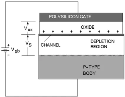
charge in the silicon increases to include electrons as well as ionized acceptors. The electrons are mobile and can contribute to current flow. A positive gate voltage reduces electron energy in the silicon under the gate. This can be represented using the band diagram shown inFigure 1.13. With electrons as carriers in the p-type silicon, the channel is said to be inverted. It is convenient to define the onset of moderate inversion to be when the bands at the silicon surface at the oxide interface are 2φf below their values in the bulk away from the surface. The surface is at a voltage 2φf above the bulk due to the influence of the gate. Recall that voltage is energy per unit charge. Since electrons have a negative charge, when electron energy decreases, voltage increases. Alsoφf, the Fermi energy, is the position of the intrinsic energy level relative to the Fermi level in the bulk semiconductor as shown inFigure 1.13.
The gate to bulk voltage at the onset of moderate inversion is the sum of:
1. The surface potentialVs. This is the voltage at the oxide interface relative to the bulk.
2. The voltage across the oxide.
3. The contact potential between the gate and the bulk Φms. VGB=Vs+Vox+ Φms (1.70) At the onset of moderate inversionVs = 2φf as shown inFigure 1.13. The voltage across the oxide is the electric field in the oxide multiplied by the oxide thicknesstox. From Gauss’ law, the electric field in the oxide is the charge per unit area on the gate divided by the oxide permittivity: Eox=QG/ǫox. The voltage across the oxide is
Vox=Eoxtox=QG
Since the positive charge on the gate must be balanced by negative charge in the silicon and in the oxide
QG =QB−Qox+QI (1.72) whereQB is the charge due to ionized acceptors in the depletion region. QB =qNAxdwhereNAis the substrate doping andxdis the width of the depletion region. Qox is positive charge trapped in the oxide. Here we assumeQoxis all trapped at the oxide silicon interface. QI is charge due to mobile electrons in the channel. At the onset of moderate inversion, QI is small and does not contribute to QG. The charge QB, due to ionized acceptors in the depletion region depends on Vs, the surface potential. Vsis the amount the bands are bent. Vsis the voltage across the depletion region. Equation 1.24 describing the depletion region in a pn junction can be used to determine the width of the depletion region and the chargeQB
QB =2qNAǫVs At the onset of moderate inversionVs= 2φf
QB =
4qNAǫφf From Equations 1.70, 1.71 and 1.72
VGB= Φms+Vs+
QB−Qox
ǫox tox (1.73) Since the gate capacitance per unit area is
Cox= tox ǫox
VGB = Φms+Vs+
QB−Qox Cox
At the onset of moderate inversionVs= 2φf.
VGB= Φms− Qox
Cox + 2φf+
4qNAǫφf
Cox (1.74)
VGB, given in Equation 1.74, is the gate to bulk voltage at the threshold, when the transistor begins to turn on. When the bulk is connected to the sourceVGB, the gate to bulk voltage at the onset of moderate inversion isVT O, the gate to source threshold voltage at zero bulk bias
VT O= Φms− Qox
Cox + 2φf+γ
Figure 1.14 The gate to body voltage,VGB is the sum of the surface
po-tential,Vs, the voltage across the oxide,V ox, and the body to gate contact
potential Φms.
whereγ=√2qNAǫ/Cox. γ(GAMMA) is the body effect parameter. The contact potential between the gate and the bulk Φmscontributes to the gate voltage. Consider Figure 1.14. When the gate is shorted to the bulk, VGB = 0, there is an internal contact potential that can be expressed in terms of the positions of the Fermi levels relative to the intrinsic level in the polysilicon gate and the bulk. In the bulk, the position of the Fermi level relative to the intrinsic level is φf. In the gate, the position of the Fermi level depends on the gate material. The two cases of interest for MOS transistors are polysilicon gates heavily doped either n-type or p-type. For n-type poly gates the Fermi level approaches the conduction band and isEg/2 above the intrinsic level. For p-type gates the Fermi level approaches the valence band and is Eg/2 below the intrinsic level. When the gate is shorted to the bulk, charge moves and the energy bands adjust so the Fermi levels will be the same in both materials. This results in a contact potential of
Φms=± Eg
2 −φf (1.76)
where Eg/2 is positive for p-type poly gates and negative for n-type poly gates. When the gate is a metal instead of polysilicon, this contact potential would be expressed as the difference in the work functions of the gate and bulk.
realize circuit functions. Figure 1.15 shows one CMOS implementation with an NMOS transistor in a p-well and a PMOS transistor in the n-type epitaxial layer. While most of the discussion in this chapter involves the NMOS transistor, the PNOS transistor functions in the same way with the difference that diffusion types are reversed. N-type is replaced by p-type, and p-type is replaced by n-type. Voltage polarities and current directions are also reversed. Current flow in the channel of PMOS transistors is due to holes rather than electrons. As more holes are attracted to the channel, the more negative the gate to source voltage becomes. This complementary nature of NMOS and PMOS transistors is useful in the design of analog and digital circuits.
Figure 1.15 CMOS structure.
1.6.1
Simple MOS Model
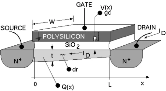
A simple model for the MOS transistor, useful for hand calculations, can be derived by considering the channel to be a variable resistor whose value depends on the gate to channel voltage, then summing the voltage across this channel resistance from the source to the drain.
Here we use the source as the voltage reference point by setting the source voltage equal to zero. With the source as the voltage reference, Vg=Vgs. The drain currentIDflowing in the channel causes the channel voltageVcs, and therefore the gate to channel voltageVgcto be a function of the distance xfrom the source as shown in Figure 1.16. Vgc is the voltage across the oxide. The channel consists of electrons attracted by the positive gate voltage. The mobile charge in the channel is
Figure 1.16 The channel resistance varies withxbecause channel voltage and therefore mobile charge varies withx.
Vds. Therefore, since the largest value ofVcs isVds,Vgs−Vth must be greater thanVdsfor this derivation to hold. Otherwise, at the drain end of the channel where the channel voltage is the greatest, there will be no mobile charge. The resistive channel can be represented as a series of small resistancesdr. The current ID flowing through these resistances causes the voltage drop in the channel. The voltage across each of these incremental resistances isdVcs=IDdrwhere dr=dx/(σtW) where W is the width of the gate andσis the conductivity of the channel andt is the effective channel thickness.
σ= charge per unit volume times the mobility σ=µQ(x)
t
whereQ(x) is the mobile channel charge per unit gate area.Q(x)/tis the mobile channel charge per unit volume. Therefore,dr=dx/[µQ(x)W]. Using Equation 1.77 forQ(x)
dVcs= IDdx
µW Cox(Vgs−Vcs−Vth)
Rearrange and integrate L
0
IDdx= Vds
0
µW Cox(Vgs−Vth−Vcs)dVcs
ID=µCox(W/L)
(Vgs−Vth)Vds−V 2 ds 2
ID increases as Vds increases to a maximum value that occurs when Vds=Vgs−Vth.
Saturation
Drain current is self limiting. As the drain to source voltage Vds increases, drain current increases. This increases the channel voltage reducing the gate to channel voltage and the mobile channel charge. WhenVds > Vgs−Vt, Q(x) vanishes at the drain end of the channel causing the transistor to operate in the saturation or constant current region. Voltages applied to the drain are absorbed across the channel-drain depletion region where no mobile charge exists. The channel-drain is more positive than the channel. Channel electrons entering this depletion region are swept into the drain by the built-in potential and the voltage applied to the drain. Since increases in drain voltages appear across the drain-channel depletion region, channel voltages and therefore channel current does not change with drain voltage. The drain current remains constant with changes in drain voltage.
With all voltages referenced to the source, Vg becomes Vgs and the drain current is
ID=
µnCox(Vgs−Vth)Vds−V 2 ds 2
Vds≤Vgs−Vth
µnCox
2 (Vgs−Vth) 2
Vds≥Vgs−Vth
(1.78)
Equation 1.78 is a simple model useful for hand calculations.
1.7
DMOS Transistors
Figure 1.17 A double diffused DMOS transistor is fabricated by diffusing first a p-well into the n-type epi through a hole in the polysilicon. A second n-type diffusion forms the source. The epi acts as drain and the channel forms in the p-well. Channel length depends on lateral diffusion of the p-well and the n-type source.
source. The drain contact is made to the epi. Arrays of these devices result in efficient layouts for power transistors.
1.8
Zener Diodes
Figure 1.18 A. The deep lying pn junction formed by the buried layer and the isolation diffusion breaks down at about 12 V and can conduct large currents. B. The pn junction formed at the surface using shallow-n (SN) and shallow-p (SP) diffusions breaks down at about 6 V.
1.9
EpiFETs
Large value resistors can be achieved by enhancing the sheet resistance of the epitaxial layer with a junction field effect transistor called an
epiFET.
Figure 1.19 Current flow in the n-type epitaxial region is restricted by the depletion region associated with the base-epi pn junction. Sheet resistance of the epiFET can be significantly higher than the epi sheet resistance.
Figure 1.20 Measured epiFET characteristics are shown. The threshold voltage VTO is about -20 V. The constant current region isV ds > V gs−Vth.
ForV gs=−3, the constant current region starts at aboutV ds= 17V. [7]
the width of the depletion region. No buried layer is present because it would short out the epiFET.
In a typical configuration three regions, the gate, isolation well and the substrate are connected to the negative supply. As the epi becomes more positive, the depletion regions from all three regions extend into the epi reducing the cross-section for current flow.
1.10
Chapter Exercises
1. Calculate the resistivity of silicon doped with 5x10¹⁸ phospho-rus(group 5) atoms per cubic centimeter. Assume total ionization. 2. Calculate the conductivity of intrinsic silicon.
3. Show that
Jn=qµnE is equivalent to Ohm’s law.
4. Calculate the position of the Fermi level relative to the intrinsic level for the silicon in problem 1.
5. A silicon wafer is doped with 1016 acceptors per cm3 and then doped with 5x10¹⁷donors per cubiccm3. What is the resistivity? Estimate mobility usingFigure 1.2.
6. Consider a silicon pn junction. The p-side is uniformly doped with 1018
acceptors/cm3
. The n-side is doped with 1016
Figure 1.21 Figure for problem 9.
What is the position of the Fermi level relative to the intrinsic level on the p-side of the junction?
7. For the pn junction in problem 6, the junction area is 10 microns by 10 microns. What is the saturation currentIs. Use mobility vs doping curves (Figure 1.2).
8. Consider a pn junction with the P-side doped withNA= 1020cm−3. Approximately, what is the required doping on the N-side to obtain a breakdown of 20 V? Use the one-sided step junction approxima-tion.
9. A 10 K resistor is in series with an NMOS transistor as shown in Figure 1.21: [W/L]µnCox= 10−5. The threshold voltage is one volt. What is the output voltage, Vo?
References
[1] S. M. Sze and J. C. Irvin,Resistivity, Mobility and Impurity Levels in GaAs, Ge, and Si at 300◦K, Solid-State Electronics, Vol 11, pp. 599-602, 1968.
[2] S. M. Sze, Physics of Semiconductor Devices, Wiley-Interscience, New York, 1969.
[3] Edward S. Yang,Microelectronic Devices, McGraw-Hill, New York, 1988.
[4] P.R. Gray and R.G. Meyer, Analysis and Design of Analog Inte-grated Circuits, 2nd edition, Wiley, New York, c. 1984, pp. 1-5. [5] R.S. Muller and T.I. Kamins,Device Electronics for Integrated
Cir-cuits, 2nd edition, Wiley, New York, c. 1986, pp. 15-27, 173-188, 235-244.
[6] K. Lee, M. Shur, T.A. Fjeldy and T. Ytterdal,Semiconductor De-vice Modeling for VLSI, Prentice Hall, Englewood Cliffs, NJ, c. 1993, p. 63.
chapter 2
Device Models
2.1
Introduction
Models are mathematical descriptions that predict performance. They can be physical or empirical. Physical models are based on device physics and can be related to physical properties. Empirical models fit measure-ments to mathematical descriptions that do not necessarily correspond to device physics. Physical models are easier to adapt when parameters such as doping levels or device dimensions change.
Modeling is a tradeoff between accuracy and utility. Exact models tend to be more complex than approximate ones. The model to use is the simplist one that provides the required accuracy. Models for hand calculation, where computational power is limited, should be simple. Even with high speed computers, complex models can make the simula-tions of large systems prohibitive.
2.2
Bipolar Transistors
2.2.1
Early Effect
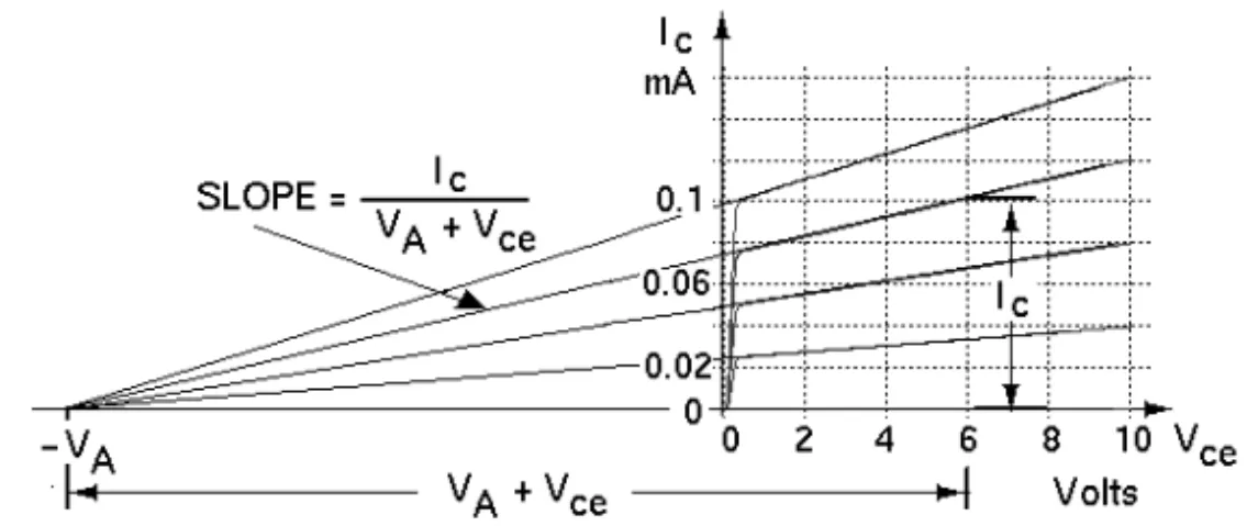
Increasing the voltage across the transistorVCE results in an increase in transistor currentIC. The physical cause, is a decrease in the width of the base. AsVCE is increased, the reverse voltage on the collector-base pn junction increases. The collector-collector-base depletion region extends further into the base, effectively reducing the base width. Since collector current varies inversely with base width, collector current increases. The slope ofIC vs. VCE in the normal operation range is modeled by the Early voltage as shown inFigure 2.1.
2.2.2
High Level Injection
Figure 2.1 The dependence ofIC onVCEis described by the Early voltage
VA.
cause collector current to be less than predicted by Equation 1.52. AsVBE is increased, large numbers of electrons are injected into the base from the emitter. High level injection is defined to be when the density of electrons in the base approaches the density of acceptor atoms in the base. Extra positive voltage has to be applied to the base in order to maintain the negative charge density in the base which is produced by the high level injection of electrons from the emitter. VBE is distributed between the junction and across the base region containing the high level of injected electrons. Only a portion of the voltage applied to the base and emitter terminals, VBE, appears across the base emitter junction. Therefore,VBEis not as effective in increasing injection across the base-emitter junction. The result isICproportional toexp(VBE/2VT). That is, collector current does not increase as fast with increases inVBE as it does in low level injection. The reduction in collector current results in a reduction inβ. At low current levels, the component of base current due to spontaneous generation of electron hole pairs in the base emitter depletion region becomes significant. This component of base current varies aseVBE/2VT. It represents base current that does not contribute to collector current. This results in a decrease inβ at low current levels as shown inFigure 2.2.
2.2.3
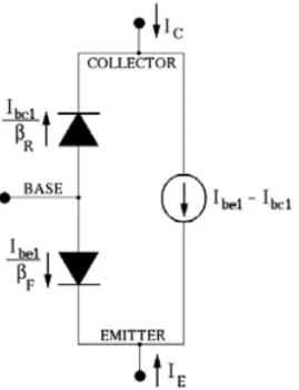
Gummel-Poon Model
The Gummel-Poon model, like the Ebers-Moll, is not limited to positive base-emitter and positive collector-emitter voltages, but is valid for both positive and negative applied voltages. This is accomplished in a seam-less way with one set of equations. Gummel-Poon was an improvement over the Ebers-Moll model in that it took into account the Early and high level injection effects.
Figure 2.2 The current gain,β, of an npn transistor is shown. Gain drops off at low and high collector current. Note the logarithmic nature of the horizontal axis.
Ipe), and in Equation 1.54,IC=Inc−Ipc. Positive currents are defined to flow into a terminal. Inc is the component of collector current due to electrons. These electrons are injected from the emitter and diffuse across the base to the collector. They contribute to both the collector and emitter currents. Ipc is the component of collector current due to holes injected from the base into the collector. Ipe is the component of emitter current due to holes injected from the base to the emitter. In this simple description where recombination in the base is considered small and ignored, Ipe is equal to the base current when the transistor is biased in normal forward operation with the base-emitter junction forward biased and the base-collector junction reversed biased.
From Equation 1.56
Inc=Is
eVBEVT −e Vbc VT
(2.1)
where
Is= AEqDnn 2 i
WBNA (2.2)
Define
Ibe1=Is
eVBEVT −1
Figure 2.3 Gummel-Poon npn model without the Early effect and high level injection effects.
and
Ibc1=Is
eVCEVT −1
(2.4)
then
Inc=Ibe1−Ibc1 (2.5)
Also, in the normal forward operating region,Ibe1is the collector current andIpe is the base current. Therefore,
Ibe1=βFIpe (2.6)
The equations are symmetric so that in the reverse condition
Ibc1=βRIpc (2.7)
Using Equations 2.1 thru 2.7 in Equations 1.53 and 1.54 yields the following
IE=−(Ibe1−Ibc1)−Ipe
βF (2.8)
IC=Ibe1−Ibc1− Ice
βR (2.9)
Figure 2.4 The Gummel-Poon model usesKqb to describe high level in-jection and low level effects and the Early effect and the currents Ibe2 and Ibc2 to describe low level effects due to generation and recombination in the depletion regions.
base. When the collector voltage increases, Kqb becomes smaller be-cause the base collector depletion region increases, reducing the base width and therefore the charge in the base. This is the Early effect. It causes the collector current to increase. When there is a high level of injected holes from the emitter, the extra electrons attract extra holes, increasing the positive mobile charge in the base. If the density of these added charges approaches the doping level in the base, the voltage nec-essary to maintain the positive charge becomes important. A portion of the applied base-emitter voltage appears across the positive charge in the base and is not available to the base-emitter junction. This is the high level injection effect. It causes collector current to be less than would be expected. High level injection is modeled as an increase in Kqb. Adding the base charge factorKqbto Equations 2.8 and 2.9 yields
IE=−Ibe1−Ibc1
Kqb −
Ipe
βF (2.10)
IC= Ibe1−Ibc1
Kqb −
Ice
βR (2.11)
Equations 2.10 and 2.11 are illustrated inFigure 2.4. Also shown in
These currents model base current due to recombination in the depletion regions.
Base to emitter and base to collector capacitance is also shown in
Figure 2.4. These capacitances are the sum of the junction and diffusion capacitance for the junctions.
Collector and base currents are plotted inFigure 2.5, called a Gummel plot. The logarithmic vertical axis results in a straight line plot, with a slope of 1/VT over a wide range. This is true since
IC =IseVBEVT
ln(IC) =ln(Is) +VBE VT
Since the logarithms of the collector and base currents are plotted in
Figure 2.5, the log of β, the ratio ofIC to IB, is the distance between the curves ln(IC)−ln(IB). β decreases at both high and low values of collector current. At high levels, collector current is reduced by high level injection effects. The plot of collector current is a straight line up to about the forward knee current,IKF. At larger current values high level injection effects reduce the slope of the current plot to a value close toVT/2. At low current levels, base current is larger than expected due to recombination and generation current. This current is represented by Ibe2 flowing in the diode in Figure 2.4. It does not contribute to the collector current. The variation ofβ with collector current is plotted in
Figure 2.2.
2.3
MOS Transistors
MOS transistors in the 1960s could be modeled using the simple equa-tions for hand calculaequa-tions, such as Equation 1.78 discussed in Chapter 1. Model parameters corresponded to physical quantities and could be extracted from the data of simple experiments. As technology evolved, the situation became more complex due to the effects of small geome-tries and high fields. Model equations have become more complicated and the number of parameters required to describe effects has increased. With more complex effects to be described and larger numbers of param-eters, the link between the model parameters and their physical basis has become obscure. Model parameters can be divided into two groups.
to measured data,