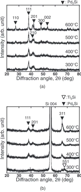
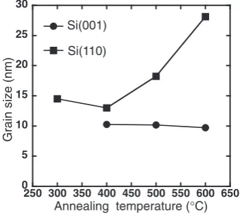
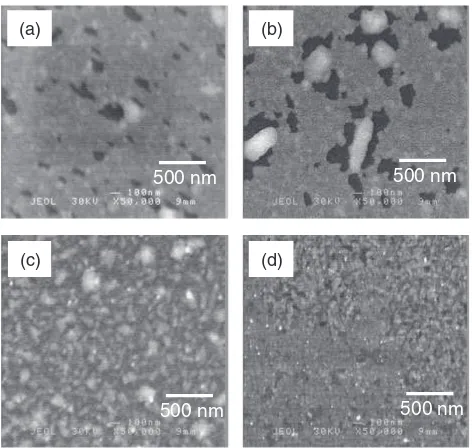
Formation of Palladium Silicide Thin Layers on Si(110) Substrates
Bebas
5
0
0
Teks penuh
Gambar
Dokumen terkait
